

Page 1
64 Kb I2C CMOS Serial
EEPROM
CAT24C64
Description
The CAT24C64 is a 64 Kb CMOS Serial EEPROM device,
internally organized as 8192 words of 8 bits each.
It features a 32−byte page write buffer and supports the Standard
(100 kHz), Fast (400 kHz) and Fast−Plus (1 MHz) I
External address pins make it possible to address up to eight
CAT24C64 devices on the same bus.
Features
• Supports Standard, Fast and Fast−Plus I
2
C Protocol
• 1.7 V to 5.5 V Supply Voltage Range
• 32−Byte Page Write Buffer
• Hardware Write Protection for Entire Memory
• Schmitt Triggers and Noise Suppression Filters on I
(SCL and SDA)
• Low Power CMOS Technology
• 1,000,000 Program/Erase Cycles
• 100 Year Data Retention
• Industrial and Extended Temperature Range
• SOIC, TSSOP, UDFN 8−pad and Ultra−thin WLCSP 4−bump
Packages
• This Device is Pb−Free, Halogen Free/BFR Free, and RoHS
Compliant
V
CC
SCL
A2, A1, A
0
CAT24C64
SDA
2
C protocol.
2
C Bus Inputs
www.onsemi.com
SOIC−8
W SUFFIX
CASE 751BD
UDFN−8
HU4 SUFFIX
CASE 517AZ
C4C SUFFIX
CASE 567JY
TSSOP−8
Y SUFFIX
CASE 948AL
WLCSP−4
PIN CONFIGURATIONS (Top Views)
0
1
2
UDFN (HU4)
1
A
A
A
V
SS
SOIC (W), TSSOP (Y),
V
CC
WP
SCL
SDA
MARKING
DIAGRAMS
(WLCSP−4)
X = Specific Device Code
= (see ordering information)
Y = Production Year (Last Digit)
M = Production Month (1−9, O, N, D)
W = Production Week Code
For the location of Pin 1, please consult the
corresponding package drawing.
1
V
A1 A2
CC
SCL
B1 B2
(C4C) (C4U)
X
YM
WLCSP−4
C4U SUFFIX
CASE 567PB
V
SDA
WLCSP
X
YW
SS
WP
V
SS
Figure 1. Functional Symbol
© Semiconductor Components Industries, LLC, 2018
March, 2021 − Rev. 28
PIN FUNCTION
FunctionPin Name
Device AddressA0, A1, A
2
Serial DataSDA
Serial ClockSCL
Write ProtectWP
CC
SS
Power SupplyV
GroundV
ORDERING INFORMATION
See detailed ordering and shipping information in the package
dimensions section on page 8 of this data sheet.
For serial EEPROM in a US8 package, please
consult the N24C64 datasheet.
1 Publication Order Number:
CAT24C64/D
Page 2
CAT24C64
Table 1. ABSOLUTE MAXIMUM RATINGS
Parameters Ratings Units
Storage Temperature –65 to +150 °C
Voltage on Any Pin with Respect to Ground (Note 1) –0.5 to +6.5 V
Stresses exceeding those listed in the Maximum Ratings table may damage the device. If any of these limits are exceeded, device functionality
should not be assumed, damage may occur and reliability may be affected.
1. The DC input voltage on any pin should not be lower than −0.5 V or higher than V
undershoot to no less than −1.5 V or overshoot to no more than V
+ 1.5 V, for periods of less than 20 ns.
CC
Table 2. RELIABILITY CHARACTERISTICS (Note 2)
Symbol
N
(Note 3) Endurance 1,000,000 Program/Erase Cycles
END
T
DR
Data Retention 100 Years
2. These parameters are tested initially and after a design or process change that affects the parameter according to appropriate AEC−Q100
and JEDEC test methods.
3. Page Mode, V
= 5 V, 25°C.
CC
Parameter Min Units
Table 3. D.C. OPERATING CHARACTERISTICS
(V
= 1.8 V to 5.5 V, TA = −40°C to +125°C and VCC = 1.7 V to 5.5 V, TA = −40°C to +85°C, unless otherwise specified.)
CC
Symbol
I
CCR
I
CCW
I
SB
I
L
V
IL
V
IH
V
OL1
V
OL2
Parameter Test Conditions Min Max Units
Read Current Read, f
Write Current Write, f
Standby Current All I/O Pins at GND or V
= 400 kHz 1 mA
SCL
= 400 kHz 2 mA
SCL
CC
TA = −40°C to +85°C
V
CC
TA = −40°C to +85°C
V
CC
TA = −40°C to +125°C 5
I/O Pin Leakage Pin at GND or V
CC
Input Low Voltage −0.5 VCC x 0.3 V
Input High Voltage VCC x 0.7 VCC + 0.5 V
Output Low Voltage VCC ≥ 2.5 V, IOL = 3.0 mA 0.4 V
Output Low Voltage VCC < 2.5 V, IOL = 1.0 mA 0.2 V
+ 0.5 V. During transitions, the voltage on any pin may
CC
1 mA
≤ 3.3 V
3
> 3.3 V
2
mA
Table 4. PIN IMPEDANCE CHARACTERISTICS
(VCC = 1.8 V to 5.5 V, TA = −40°C to +125°C and VCC = 1.7 V to 5.5 V, TA = −40°C to +85°C, unless otherwise specified.)
Symbol
Parameter Conditions Max Units
CIN (Note 4) SDA I/O Pin Capacitance VIN = 0 V 8 pF
CIN (Note 4) Input Capacitance (other pins) VIN = 0 V 6 pF
IWP (Note 5) WP Input Current
VIN < VIH, VCC = 5.5 V 130 mA
VIN < VIH, VCC = 3.3 V 120
VIN < VIH, VCC = 1.8 V 80
V
IA (Note 5) Address Input Current
(A0, A1, A2)
Product Rev F
> V
IN
IH
VIN < VIH, VCC = 5.5 V 50 mA
VIN < VIH, VCC = 3.3 V 35
2
VIN < VIH, VCC = 1.8 V 25
V
> V
IN
IH
2
4. These parameters are tested initially and after a design or process change that affects the parameter according to appropriate AEC−Q100
and JEDEC test methods.
5. When not driven, the WP, A0, A1 and A2 pins are pulled down to GND internally. For improved noise immunity, the internal pull−down is relatively
strong; therefore the external driver must be able to supply the pull−down current when attempting to drive the input HIGH. To conserve power,
as the input level exceeds the trip point of the CMOS input buffer (~ 0.5 x V
), the strong pull−down reverts to a weak current source.
CC
www.onsemi.com
2
Page 3
CAT24C64
Table 5. A.C. CHARACTERISTICS
(VCC = 1.8 V to 5.5 V, TA = −40°C to +125°C and VCC = 1.7 V to 5.5 V, TA = −40°C to +85°C.) (Note 6)
Fast−Plus
= 1.7 V − 5.5 V
V
CC
= −405C to +855C
T
A
Units
ms
ms
ms
ms
ms
ms
ms
ms
ms
ms
Symbol
F
SCL
t
HD:STA
t
LOW
t
HIGH
t
SU:STA
t
HD:DAT
t
SU:DAT
Standard
= 1.7 V − 5.5 V
V
CC
Parameter
Min Max Min Max Min Max
Clock Frequency 100 400 1,000 kHz
START Condition Hold Time 4 0.6 0.25
Low Period of SCL Clock 4.7 1.3 0.45
High Period of SCL Clock 4 0.6 0.40
START Condition Setup Time 4.7 0.6 0.25
Data In Hold Time 0 0 0
Data In Setup Time 250 100 50 ns
Fast
= 1.7 V − 5.5 V
V
CC
tR (Note 7) SDA and SCL Rise Time 1,000 300 100 ns
tF (Note 7) SDA and SCL Fall Time 300 300 100 ns
t
SU:STO
t
BUF
t
AA
t
DH
Ti (Note 7) Noise Pulse Filtered at SCL
STOP Condition Setup Time 4 0.6 0.25
Bus Free Time Between
4.7 1.3 0.5
STOP and START
SCL Low to Data Out Valid 3.5 0.9 0.40
Data Out Hold Time 100 100 50 ns
100 100 100 ns
and SDA Inputs
t
SU:WP
t
HD:WP
t
WR
WP Setup Time 0 0 0
WP Hold Time 2.5 2.5 1
Write Cycle Time 5 5 5 ms
tPU (Notes 7, 8) Power−up to Ready Mode 1 1 0.1 1 ms
Product parametric performance is indicated in the Electrical Characteristics for the listed test conditions, unless otherwise noted. Product
performance may not be indicated by the Electrical Characteristics if operated under different conditions.
6. Test conditions according to “A.C. Test Conditions” table.
7. Tested initially and after a design or process change that affects this parameter.
is the delay between the time VCC is stable and the device is ready to accept commands.
8. t
PU
Table 6. A.C. TEST CONDITIONS
Input Levels 0.2 x VCC to 0.8 x V
Input Rise and Fall Times ≤ 50 ns
Input Reference Levels 0.3 x VCC, 0.7 x V
Output Reference Levels 0.5 x V
CC
Output Load Current Source: IOL = 3 mA (VCC ≥ 2.5 V); IOL = 1 mA (V
CC
CC
www.onsemi.com
3
< 2.5 V); CL = 100 pF
CC
Page 4
CAT24C64
Power−On Reset (POR)
Each CAT24C64 incorporates Power−On Reset (POR)
circuitry which protects the internal logic against powering
up in the wrong state. The device will power up into Standby
mode after V
power down into Reset mode when V
exceeds the POR trigger level and will
CC
drops below the
CC
POR trigger level. This bi−directional POR behavior
protects the device against ‘brown−out’ failure following a
temporary loss of power.
Pin Description
SCL: The Serial Clock input pin accepts the clock signal
generated by the Master.
SDA: The Serial Data I/O pin accepts input data and delivers
output data. In transmit mode, this pin is open drain. Data is
acquired on the positive edge, and is delivered on the
negative edge of SCL.
A
, A1 and A2: The Address inputs set the device address
0
that must be matched by the corresponding Slave address
bits. The Address inputs are hard−wired HIGH or LOW
allowing for up to eight devices to be used (cascaded) on the
same bus. When left floating, these pins are pulled LOW
internally. The Address inputs are not available for use with
WLCSP 4−bumps.
WP: When pulled HIGH, the Write Protect input pin
inhibits all write operations. When left floating, this pin is
pulled LOW internally. The WP input is not available for the
WLCSP 4−bumps, therefore all write operations are allowed
for the device in this package.
transmit or receive, but only the Master can assign those
roles.
I2C Bus Protocol
The 2−wire I2C bus consists of two lines, SCL and SDA,
connected to the V
supply via pull−up resistors. The
CC
Master provides the clock to the SCL line, and either the
Master or the Slaves drive the SDA line. A ‘0’ is transmitted
by pulling a line LOW and a ‘1’ by letting it stay HIGH. Data
transfer may be initiated only when the bus is not busy (see
A.C. Characteristics). During data transfer, SDA must
remain stable while SCL is HIGH.
START/STOP Condition
An SDA transition while SCL is HIGH creates a START
or STOP condition (Figure 2). The START consists of a
HIGH to LOW SDA transition, while SCL is HIGH. Absent
the START, a Slave will not respond to the Master. The
STOP completes all commands, and consists of a LOW to
HIGH SDA transition, while SCL is HIGH.
Device Addressing
The Master addresses a Slave by creating a START
condition and then broadcasting an 8−bit Slave address. For
the CAT24C64, the first four bits of the Slave address are set
to 1010 (Ah); the next three bits, A
, A1 and A0, must match
2
the logic state of the similarly named input pins. The devices
in WLCSP 4−bumps respond only to the Slave Address with
A2 A1 A0 = 000 (CAT24C64C4xTR). The R/W bit tells the
Slave whether the Master intends to read (1) or write (0) data
(Figure 3).
Functional Description
The CAT24C64 supports the Inter−Integrated Circuit
2
(I
C) Bus protocol. The protocol relies on the use of a Master
device, which provides the clock and directs bus traffic, and
Slave devices which execute requests. The CAT24C64
operates as a Slave device. Both Master and Slave can
SCL
SDA
START
CONDITION
Figure 2. Start/Stop Timing
1010
* The devices in WLCSP 4−bumps respond only to the Slave Address with: A2 A1 A0 = 000, CAT24C64C4xTR
Figure 3. Slave Address Bits
Acknowledge
During the 9th clock cycle following every byte sent to the
bus, the transmitter releases the SDA line, allowing the
receiver to respond. The receiver then either acknowledges
(ACK) by pulling SDA LOW, or does not acknowledge
(NoACK) by letting SDA stay HIGH (Figure 4). Bus timing
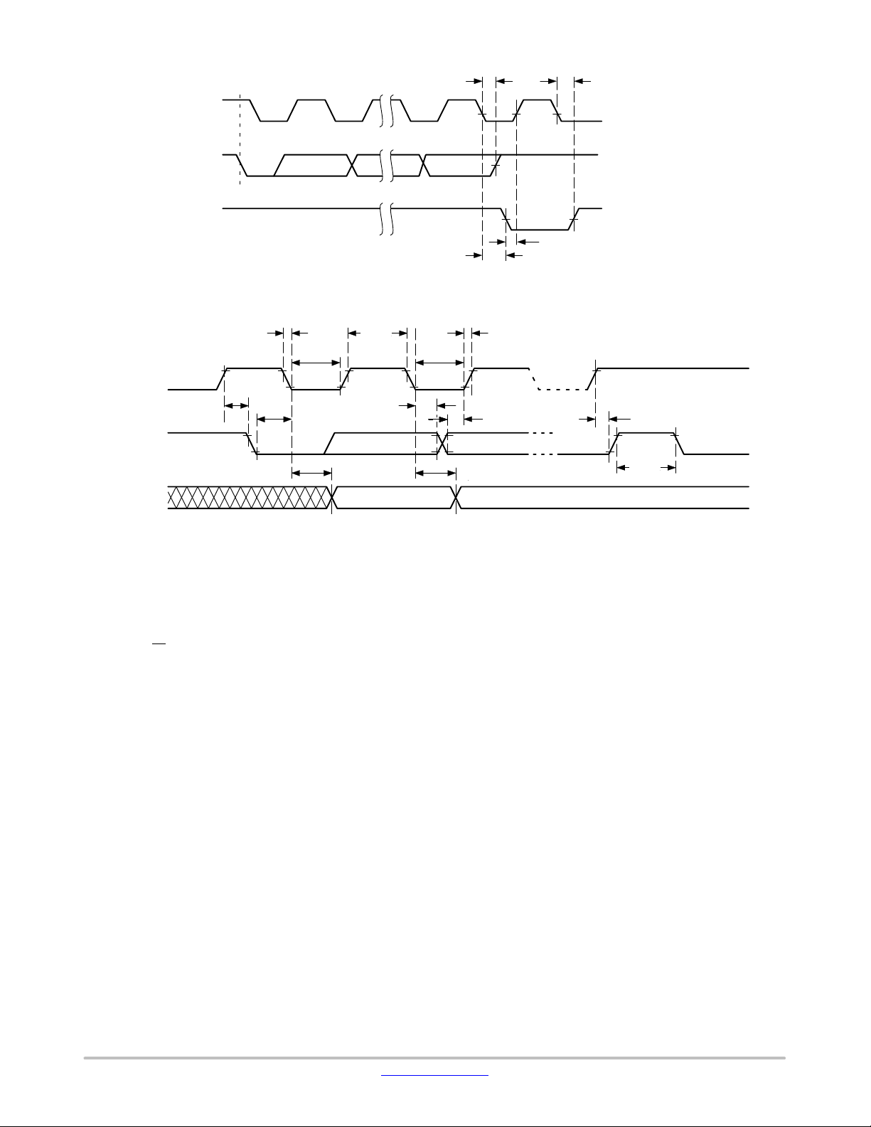
is illustrated in Figure 5.
STOP
CONDITION
A2A1A0R/W
DEVICE ADDRESS*
www.onsemi.com
4
Page 5
CAT24C64
SCL FROM
MASTER
DATA OUTPUT
FROM TRANSMITTER
DATA OUTPUT
FROM RECEIVER
SCL
t
SU:STA
SDA IN
SDA OUT
BUS RELEASE DELAY (TRANSMITTER)
189
START
ACK DELAY (≤ t
Figure 4. Acknowledge Timing
t
F
t
LOW
t
HD:STA
t
HIGH
t
HD:DAT
t
AA
t
LOW
AA
BUS RELEASE DELAY (RECEIVER)
)
t
R
t
SU:DAT
t
DH
ACK SETUP (≥ t
SU:DAT
t
SU:STO
t
BUF
)
Figure 5. Bus Timing
WRITE OPERATIONS
Byte Write
To write data to memory, the Master creates a START
condition on the bus and then broadcasts a Slave address
with the R/W
bit set to ‘0’. The Master then sends two
address bytes and a data byte and concludes the session by
creating a STOP condition on the bus. The Slave responds
with ACK after every byte sent by the Master (Figure 6). The
STOP starts the internal Write cycle, and while this
operation is in progress (t
), the SDA output is tri−stated
WR
and the Slave does not acknowledge the Master (Figure 7).
Page Write
The Byte Write operation can be expanded to Page Write,
by sending more than one data byte to the Slave before
issuing the STOP condition (Figure 8). Up to 32 distinct data
bytes can be loaded into the internal Page Write Buffer
starting at the address provided by the Master. The page
address is latched, and as long as the Master keeps sending
data, the internal byte address is incremented up to the end
of page, where it then wraps around (within the page). New
data can therefore replace data loaded earlier. Following the
STOP, data loaded during the Page Write session will be
written to memory in a single internal Write cycle (t
WR
).
Acknowledge Polling
As soon (and as long) as internal Write is in progress, the
Slave will not acknowledge the Master. This feature enables
the Master to immediately follow−up with a new Read or
Write request, rather than wait for the maximum specified
Write time (t
) to elapse. Upon receiving a NoACK
WR
response from the Slave, the Master simply repeats the
request until the Slave responds with ACK.
Hardware Write Protection
With the WP pin held HIGH, the entire memory is
protected against Write operations. If the WP pin is left
floating or is grounded, it has no impact on the Write
operation. The state of the WP pin is strobed on the last
falling edge of SCL immediately preceding the 1
st
data byte
(Figure 9). If the WP pin is HIGH during the strobe interval,
the Slave will not acknowledge the data byte and the Write
request will be rejected.
Delivery State
The CAT24C64 is shipped erased, i.e., all bytes are FFh.
www.onsemi.com
5
Page 6

CAT24C64
SCL
SDA
BUS
ACTIVITY:
MASTER
SLAVE
BUS ACTIVITY:
MASTER
SLAVE
*a15 − a13 are don’t care bits.
Byte n
S
T
A
SLAVE
R
ADDRESS
T
S
A
C
K
S
T
A
R
ADDRESS
T
S
ADDRESS
BYTE
SLAVE
ADDRESS
ADDRESS
BYTE
− a
a
15
8
***
A
C
K
A
C
K
Figure 6. Byte Write Sequence
ACK8th Bit
STOP
CONDITION
Figure 7. Write Cycle Timing
DATA
BYTE
A
C
K
A
C
K
ADDRESS
BYTE
BYTE
a7 − a
t
WR
n
0
A
C
K
A
C
K
DATA
BYTE
d7 − d
START
CONDITION
DATA
BYTE
n+1
S
T
O
0
P
P
A
C
K
ADDRESS
DATA
BYTE
n+P
S
T
O
P
P
A
A
C
C
K
K
A
C
K
SCL
SDA
WP
Figure 8. Page Write Sequence
ADDRESS
BYTE
t
HD:WP
1
d
7
189
a
7
a
0
t
SU:WP
Figure 9. WP Timing
DATA
BYTE
8
d
0
www.onsemi.com
6
Page 7

CAT24C64
READ OPERATIONS
Immediate Read
To read data from memory, the Master creates a START
condition on the bus and then broadcasts a Slave address
with the R/W
and starts shifting out data residing at the current address.
After receiving the data, the Master responds with NoACK
and terminates the session by creating a STOP condition on
the bus (Figure 10). The Slave then returns to Standby mode.
Selective Read
To read data residing at a specific address, the selected
address must first be loaded into the internal address register.
This is done by starting a Byte Write sequence, whereby the
Master creates a START condition, then broadcasts a Slave
address with the R/W
address bytes to the Slave. Rather than completing the Byte
bit set to ‘1’. The Slave responds with ACK
bit set to ‘0’ and then sends two
Write sequence by sending data, the Master then creates a
START condition and broadcasts a Slave address with the
R/W
bit set to ‘1’. The Slave responds with ACK after every
byte sent by the Master and then sends out data residing at
the selected address. After receiving the data, the Master
responds with NoACK and then terminates the session by
creating a STOP condition on the bus (Figure 11).
Sequential Read
If, after receiving data sent by the Slave, the Master
responds with ACK, then the Slave will continue
transmitting until the Master responds with NoACK
followed by STOP (Figure 12). During Sequential Read the
internal byte address is automatically incremented up to the
end of memory, where it then wraps around to the beginning
of memory.
SCL
SDA 8th Bit
BUS ACTIVITY:
MASTER
SLAVE
S
T
A
R
T
S
SLAVE
ADDRESS
BUS ACTIVITY:
MASTER
SLAVE
S
T
A
SLAVE
R
ADDRESS
T
S
A
DATA
C
BYTE
K
89
NO ACKDATA OUT
N
O
A
C
K
Figure 10. Immediate Read Sequence and Timing
S
T
A
SLAVE
R
T
S
A
C
K
A
C
K
ADDRESS
BYTE
ADDRESS
BYTE ADDRESS
A
C
K
Figure 11. Selective Read Sequence
S
T
O
P
P
STOP
N
O
S
T
A
O
C
P
K
P
A
DATA
C
BYTE
K
BUS ACTIVITY:
MASTER
SLAVE
SLAVE
ADDRESS
N
O
S
A
C
K
A
DATA
C
BYTE
K
n
DATA
BYTE
n+1
A
C
K
DATA
BYTE
n+2
A
C
K
DATA
BYTE
n+x
A
T
C
O
K
P
P
Figure 12. Sequential Read Sequence
www.onsemi.com
7
Page 8

CAT24C64
ORDERING INFORMATION
Specific
Device
Device Order Number
CAT24C64WI−GT3 24C64F SOIC−8, JEDEC I = Industrial
CAT24C64YI−GT3 C64F TSSOP−8 I = Industrial
CAT24C64HU4I−GT3 C6U UDFN−8 I = Industrial
CAT24C64C4CTR A WLCSP−4
CAT24C64C4UTR A WLCSP−4
9. All packages are RoHS−compliant (Lead−free, Halogen−free).
10.The standard lead finish is NiPdAu.
11.For information on tape and reel specifications, including part orientation and tape sizes, please refer to our Tape and Reel Packaging
Specifications Brochure, BRD8011/D.
12.Caution: The EEPROM devices delivered in WLCSP must never be exposed to ultra violet light. When exposed to ultra violet light
the EEPROM cells lose their stored data.
Marking
Package Type Temperature Range Lead Finish Shipping
NiPdAu Tape & Reel,
3,000 Units / Reel
NiPdAu Tape & Reel,
3,000 Units / Reel
NiPdAu Tape & Reel,
3,000 Units / Reel
N/A Tape & Reel,
5,000 Units / Reel
N/A Tape & Reel,
5,000 Units / Reel
with Die Coat
with Die Coat
(−40°C to +85°C)
(−40°C to +85°C)
(−40°C to +85°C)
Industrial
(−40°C to +85°C)
Industrial
(−40°C to +85°C)
www.onsemi.com
8
Page 9

ÉÉ
MECHANICAL CASE OUTLINE
PACKAGE DIMENSIONS
UDFN8, 2x3 EXTENDED PAD
1
SCALE 2:1
CASE 517AZ
ISSUE A
DATE 23 MAR 2015
PIN ONE
REFERENCE
NOTE 4
DETAIL A
D
C0.10
C0.10
TOP VIEW
C0.10
C0.08
SIDE VIEW
D2
1
8
e
BOTTOM VIEW
DETAIL B
A1
4
5
A
L
E2
8X
B
E
A
b
0.10 C
0.05 C
A3
M
M
C
L
L1
DETAIL A
ALTERNATE
CONSTRUCTIONS
MOLD CMPDEXPOSED Cu
DETAIL B
ALTERNATE
CONSTRUCTIONS
SEATING
PLANE
A
B
NOTE 3
RECOMMENDED
SOLDERING FOOTPRINT*
1.56
A1
L
NOTES:
1. DIMENSIONING AND TOLERANCING PER
ASME Y14.5M, 1994.
2. CONTROLLING DIMENSION: MILLIMETERS.
3. DIMENSION b APPLIES TO PLATED
TERMINAL AND IS MEASURED BETWEEN
0.15 AND 0.25MM FROM THE TERMINAL TIP.
4. COPLANARITY APPLIES TO THE EXPOSED
PAD AS WELL AS THE TERMINALS.
MILLIMETERS
DIM MIN MAX
A3
A 0.45 0.55
A1 0.00 0.05
A3 0.13 REF
b 0.20 0.30
D 2.00 BSC
D2 1.35 1.45
E 3.00 BSC
E2 1.25 1.35
e 0.50 BSC
L 0.25 0.35
L1 −−− 0.15
GENERIC
MARKING DIAGRAM*
1
XXXXX
AWLYWG
XXXXX = Specific Device Code
A = Assembly Location
WL = Wafer Lot
Y = Year
W = Work Week
G = Pb−Free Package
*This information is generic. Please refer to
device data sheet for actual part marking.
Pb−Free indicator, “G” or microdot “ G”,
may or may not be present.
8X
0.68
3.40
1.45
1
8X
0.50
PITCH
DIMENSIONS: MILLIMETERS
*For additional information on our Pb−Free strategy and soldering
details, please download the ON Semiconductor Soldering and
Mounting Techniques Reference Manual, SOLDERRM/D.
DOCUMENT NUMBER:
DESCRIPTION:
ON Semiconductor and are trademarks of Semiconductor Components Industries, LLC dba ON Semiconductor or its subsidiaries in the United States and/or other countries.
ON Semiconductor reserves the right to make changes without further notice to any products herein. ON Semiconductor makes no warranty, representation or guarantee regarding
the suitability of its products for any particular purpose, nor does ON Semiconductor assume any liability arising out of the application or use of any product or circuit, and specifically
disclaims any and all liability, including without limitation special, consequential or incidental damages. ON Semiconductor does not convey any license under its patent rights nor the
rights of others.
© Semiconductor Components Industries, LLC, 2019
98AON42552E
UDFN8, 2X3 EXTENDED PAD
Electronic versions are uncontrolled except when accessed directly from the Document Repository.
Printed versions are uncontrolled except when stamped “CONTROLLED COPY” in red.
0.30
PAGE 1 OF 1
www.onsemi.com
Page 10

MECHANICAL CASE OUTLINE
PACKAGE DIMENSIONS
SCALE 4:1
WLCSP4, 0.77x0.77
CASE 567JY
ISSUE C
DATE 07 MAR 2017
NOTE 5
0.03
PIN A1
REFERENCE
TOP VIEW
E
DETAIL A
0.05 C
0.05 C
NOTE 4
A1
SIDE VIEW
4X
b
A0.05 BC
C
B
A
12
BOTTOM VIEW
RECOMMENDED
SOLDERING FOOTPRINT*
1
A
A
A2
A
e
PACKAGE
OUTLINE
e
B
D
C
NOTE 3
SEATING
PLANE
NOTE 6
DIE COAT
(OPTIONAL)
DETAIL A
A3
NOTES:
1. DIMENSIONING AND TOLERANCING PER ASME
Y14.5M, 1994.
2. CONTROLLING DIMENSION: MILLIMETERS.
3. DATUM C, THE SEATING PLANE, IS DEFINED BY THE
SPHERICAL CROWNS OF THE SOLDER BALLS.
4. COPLANARITY APPLIES TO SPHERICAL CROWNS OF
THE SOLDER BALLS.
5. DIMENSION b IS MEASURED AT THE MAXIMUM
CONTACT BALL DIAMETER PARALLEL TO DATUM C.
6. BACKSIDE COATING IS OPTIONAL.
A2
DIMAMIN NOM
MILLIMETERS
−−−
A1
A2 0.23 REF
A3 0.025 REF
b 0.15 0.155
D
E
e 0.40 BSC
−−−
0.04 0.06
0.75 0.77
0.75 0.77
MAX
0.35
0.08
0.16
0.79
0.79
GENERIC
MARKING DIAGRAM*
X
YW
X = Specific Device Code
Y = Year
W = Work Week
*This information is generic. Please refer to
device data sheet for actual part marking.
Pb−Free indicator, “G” or microdot “ G”,
may or may not be present.
0.40
4X
0.16
0.40
PITCH
PITCH
DIMENSIONS: MILLIMETERS
*For additional information on our Pb−Free strategy and soldering
details, please download the ON Semiconductor Soldering and
Mounting Techniques Reference Manual, SOLDERRM/D.
DOCUMENT NUMBER:
DESCRIPTION:
ON Semiconductor and are trademarks of Semiconductor Components Industries, LLC dba ON Semiconductor or its subsidiaries in the United States and/or other countries.
ON Semiconductor reserves the right to make changes without further notice to any products herein. ON Semiconductor makes no warranty, representation or guarantee regarding
the suitability of its products for any particular purpose, nor does ON Semiconductor assume any liability arising out of the application or use of any product or circuit, and specifically
disclaims any and all liability, including without limitation special, consequential or incidental damages. ON Semiconductor does not convey any license under its patent rights nor the
rights of others.
© Semiconductor Components Industries, LLC, 2019
98AON85186F
WLCSP4, 0.77X0.77
Electronic versions are uncontrolled except when accessed directly from the Document Repository.
Printed versions are uncontrolled except when stamped “CONTROLLED COPY” in red.
PAGE 1 OF 1
www.onsemi.com
Page 11

MECHANICAL CASE OUTLINE
PACKAGE DIMENSIONS
SCALE 4:1
WLCSP4, 0.77x0.77
CASE 567PB
ISSUE A
DATE 09 NOV 2016
NOTE 5
0.03
PIN A1
REFERENCE
TOP VIEW
E
DETAIL A
0.05 C
0.05 C
NOTE 4
A1
SIDE VIEW
4X
b
A0.05 BC
C
B
A
12
BOTTOM VIEW
RECOMMENDED
SOLDERING FOOTPRINT*
1
A
A
A2
A
e
PACKAGE
OUTLINE
e
B
D
C
NOTE 3
SEATING
PLANE
NOTE 6
DIE COAT
(OPTIONAL)
DETAIL A
A3
NOTES:
1. DIMENSIONING AND TOLERANCING PER ASME
Y14.5M, 1994.
2. CONTROLLING DIMENSION: MILLIMETERS.
3. DATUM C, THE SEATING PLANE, IS DEFINED BY THE
SPHERICAL CROWNS OF THE SOLDER BALLS.
4. COPLANARITY APPLIES TO SPHERICAL CROWNS OF
THE SOLDER BALLS.
5. DIMENSION b IS MEASURED AT THE MAXIMUM
CONTACT BALL DIAMETER PARALLEL TO DATUM C.
6. BACKSIDE COATING IS OPTIONAL.
A2
DIMAMIN NOM
MILLIMETERS
−−−
A1
A2 0.19 REF
A3 0.025 REF
b 0.15 0.155
D
E
e 0.40 BSC
−−−
0.04 0.055
0.75 0.77
0.75 0.77
MAX
0.30
0.07
0.16
0.79
0.79
GENERIC
MARKING DIAGRAM*
X
YW
X = Specific Device Code
Y = Year
W = Work Week
*This information is generic. Please refer to
device data sheet for actual part marking.
Pb−Free indicator, “G” or microdot “ G”,
may or may not be present.
0.40
4X
0.16
0.40
PITCH
PITCH
DIMENSIONS: MILLIMETERS
*For additional information on our Pb−Free strategy and soldering
details, please download the ON Semiconductor Soldering and
Mounting Techniques Reference Manual, SOLDERRM/D.
DOCUMENT NUMBER:
DESCRIPTION:
ON Semiconductor and are trademarks of Semiconductor Components Industries, LLC dba ON Semiconductor or its subsidiaries in the United States and/or other countries.
ON Semiconductor reserves the right to make changes without further notice to any products herein. ON Semiconductor makes no warranty, representation or guarantee regarding
the suitability of its products for any particular purpose, nor does ON Semiconductor assume any liability arising out of the application or use of any product or circuit, and specifically
disclaims any and all liability, including without limitation special, consequential or incidental damages. ON Semiconductor does not convey any license under its patent rights nor the
rights of others.
98AON12765G
WLCSP4, 0.77X0.77
Electronic versions are uncontrolled except when accessed directly from the Document Repository.
Printed versions are uncontrolled except when stamped “CONTROLLED COPY” in red.
PAGE 1 OF 1
© Semiconductor Components Industries, LLC, 2019
www.onsemi.com
Page 12

MECHANICAL CASE OUTLINE
PACKAGE DIMENSIONS
E1 E
PIN # 1
IDENTIFICATION
SOIC 8, 150 mils
CASE 751BD−01
ISSUE O
DATE 19 DEC 2008
SYMBOL MIN NOM MAX
A
A1
b
c
D
E
E1
e
h
L
θ
1.35
0.10
0.33
0.19
4.80
5.80
3.80
1.27 BSC
0.25
0.40 1.27
1.75
0.25
0.51
0.25
5.00
6.20
4.00
0.50
0º 8º
TOP VIEW
D
A1
A
e
SIDE VIEW
Notes:
(1) All dimensions are in millimeters. Angles in degrees.
(2) Complies with JEDEC MS-012.
b
h
θ
c
L
END VIEW
DOCUMENT NUMBER:
DESCRIPTION:
ON Semiconductor and are trademarks of Semiconductor Components Industries, LLC dba ON Semiconductor or its subsidiaries in the United States and/or other countries.
ON Semiconductor reserves the right to make changes without further notice to any products herein. ON Semiconductor makes no warranty, representation or guarantee regarding
the suitability of its products for any particular purpose, nor does ON Semiconductor assume any liability arising out of the application or use of any product or circuit, and specifically
disclaims any and all liability, including without limitation special, consequential or incidental damages. ON Semiconductor does not convey any license under its patent rights nor the
rights of others.
© Semiconductor Components Industries, LLC, 2019
98AON34272E
SOIC 8, 150 MILS
Electronic versions are uncontrolled except when accessed directly from the Document Repository.
Printed versions are uncontrolled except when stamped “CONTROLLED COPY” in red.
PAGE 1 OF 1
www.onsemi.com
Page 13

MECHANICAL CASE OUTLINE
PACKAGE DIMENSIONS
b
E
E1
TSSOP8, 4.4x3
CASE 948AL−01
ISSUE O
SYMBOLθMIN NOM MAX
A1
A2
E1
L1
DATE 19 DEC 2008
A
0.05
0.80
b
c
D
E
e
L
0.19
0.09
2.90
6.30
4.30
0.50
0.90
3.00
6.40
4.40
0.65 BSC
1.00 REF
0.60
1.20
0.15
1.05
0.30
0.20
3.10
6.50
4.50
0.75
0º 8º
e
TOP VIEW
D
A2
SIDE VIEW
Notes:
(1) All dimensions are in millimeters. Angles in degrees.
(2) Complies with JEDEC MO-153.
A
A1
q1
L1
c
L
END VIEW
DOCUMENT NUMBER:
DESCRIPTION:
ON Semiconductor and are trademarks of Semiconductor Components Industries, LLC dba ON Semiconductor or its subsidiaries in the United States and/or other countries.
ON Semiconductor reserves the right to make changes without further notice to any products herein. ON Semiconductor makes no warranty, representation or guarantee regarding
the suitability of its products for any particular purpose, nor does ON Semiconductor assume any liability arising out of the application or use of any product or circuit, and specifically
disclaims any and all liability, including without limitation special, consequential or incidental damages. ON Semiconductor does not convey any license under its patent rights nor the
rights of others.
© Semiconductor Components Industries, LLC, 2019
98AON34428E
TSSOP8, 4.4X3
Electronic versions are uncontrolled except when accessed directly from the Document Repository.
Printed versions are uncontrolled except when stamped “CONTROLLED COPY” in red.
PAGE 1 OF 1
www.onsemi.com
Page 14

ON Semiconductor and are trademarks of Semiconductor Components Industries, LLC dba ON Semiconductor or its subsidiaries in the United States and/or other countries.
ON Semiconductor owns the rights to a number of patents, trademarks, copyrights, trade secrets, and other intellectual property. A listing of ON Semiconductor’s product/patent
coverage may be accessed at www.onsemi.com/site/pdf/Patent−Marking.pdf
ON Semiconductor makes no warranty, representation or guarantee regarding the suitability of its products for any particular purpose, nor does ON Semiconductor assume any liability
arising out of the application or use of any product or circuit, and specifically disclaims any and all liability, including without limitation special, consequential or incidental damages.
Buyer is responsible for its products and applications using ON Semiconductor products, including compliance with all laws, regulations and safety requirements or standards,
regardless of any support or applications information provided by ON Semiconductor. “Typical” parameters which may be provided in ON Semiconductor data sheets and/or
specifications can and do vary in different applications and actual performance may vary over time. All operating parameters, including “Typicals” must be validated for each customer
application by customer’s technical experts. ON Semiconductor does not convey any license under its patent rights nor the rights of others. ON Semiconductor products are not
designed, intended, or authorized for use as a critical component in life support systems or any FDA Class 3 medical devices or medical devices with a same or similar classification
in a foreign jurisdiction or any devices intended for implantation in the human body. Should Buyer purchase or use ON Semiconductor products for any such unintended or unauthorized
application, Buyer shall indemnify and hold ON Semiconductor and its officers, employees, subsidiaries, affiliates, and distributors harmless against all claims, costs, damages, and
expenses, and reasonable attorney fees arising out of, directly or indirectly, any claim of personal injury or death associated with such unintended or unauthorized use, even if such
claim alleges that ON Semiconductor was negligent regarding the design or manufacture of the part. ON Semiconductor is an Equal Opportunity/Affirmative Action Employer. This
literature is subject to all applicable copyright laws and is not for resale in any manner.
. ON Semiconductor reserves the right to make changes without further notice to any products herein.
PUBLICATION ORDERING INFORMATION
LITERATURE FULFILLMENT:
Email Requests to: orderlit@onsemi.com
ON Semiconductor Website: www.onsemi.com
TECHNICAL SUPPORT
North American Technical Support:
Voice Mail: 1 800−282−9855 Toll Free USA/Canada
Phone: 011 421 33 790 2910
Europe, Middle East and Africa Technical Support:
Phone: 00421 33 790 2910
For additional information, please contact your local Sales Representative
◊
www.onsemi.com
1
 Loading...