


EMC2DXV5T1,
EMC3DXV5T1,
EMC4DXV5T1,
EMC5DXV5T1
Preferred Devices
Dual Common
Base−Collector Bias
Resistor Transistors
NPN and PNP Silicon Surface Mount Transistors with Monolithic Bias Resistor Network
The BRT (Bias Resistor Transistor) contains a single transistor with a monolithic bias network consisting of two resistors; a series base resistor and a base−emitter resistor. These digital transistors are designed to replace a single device and its external resistor bias network. The BRT eliminates these individual components by integrating them into a single device. In the EMC2DXV5T1 series, two complementary BRT devices are housed in the SOT−553 package which is ideal for low power surface mount applications where board space is at a premium.
Features
•Simplifies Circuit Design
•Reduces Board Space
•Reduces Component Count
•These are Pb−Free Devices
MAXIMUM RATINGS (TA = 25°C unless otherwise noted, common for Q1 and Q2, − minus sign for Q1 (PNP) omitted)
Rating |
Symbol |
Value |
Unit |
|
|
|
|
Collector-Base Voltage |
VCBO |
50 |
Vdc |
Collector-Emitter Voltage |
VCEO |
50 |
Vdc |
Collector Current |
IC |
100 |
mAdc |
Stresses exceeding Maximum Ratings may damage the device. Maximum
Ratings are stress ratings only. Functional operation above the Recommended Operating Conditions is not implied. Extended exposure to stresses above the Recommended Operating Conditions may affect device reliability.
http://onsemi.com
3 |
2 |
1 |
R1
R2
Q2
R2
Q1
R1
4 |
5 |
5 

1
SOT−553
CASE 463B
MARKING DIAGRAM
|
|
Ux M G |
|
|
G |
Ux |
= |
Specific Device Code |
|
|
x = C, 3, E, or 5 |
M |
= |
Date Code |
G= Pb−Free Package
(Note: Microdot may be in either location)
ORDERING INFORMATION
See detailed ordering and shipping information in the package dimensions section on page 2 of this data sheet.
Preferred devices are recommended choices for future use and best overall value.
♥ Semiconductor Components Industries, LLC, 2007 |
1 |
Publication Order Number: |
April, 2007 − Rev. 5 |
|
EMC2DXV5T1/D |
EMC2DXV5T1, EMC3DXV5T1, EMC4DXV5T1, EMC5DXV5T1
THERMAL CHARACTERISTICS
Characteristic |
Symbol |
Max |
Unit |
ONE JUNCTION HEATED |
|
|
|
|
|
|
|
Total Device Dissipation |
PD |
|
|
TA = 25°C |
|
357 (Note 1) |
mW |
Derate above 25°C |
|
2.9 (Note 1) |
mW/°C |
|
|
|
|
Thermal Resistance, Junction-to-Ambient |
RqJA |
350 (Note 1) |
°C/W |
BOTH JUNCTIONS HEATED |
|
|
|
|
|
|
|
Total Device Dissipation |
PD |
|
|
TA = 25°C |
|
500 (Note 1) |
mW |
Derate above 25°C |
|
4.0 (Note 1) |
mW/°C |
|
|
|
|
Thermal Resistance, Junction-to-Ambient |
RqJA |
250 (Note 1) |
°C/W |
Junction and Storage Temperature |
TJ, Tstg |
−55 to +150 |
°C |
1. FR−4 @ Minimum Pad
DEVICE ORDERING INFORMATION, MARKING AND RESISTOR VALUES
|
|
Transistor 1 − PNP |
Transistor 2 − NPN |
|
|
|||
|
|
|
|
|
|
|
Shipping† |
|
Device |
Marking |
R1 (K) |
R2 (K) |
R1 (K) |
R2 (K) |
Package |
||
EMC2DXV5T1 |
|
|
|
|
|
SOT−553* |
4000 / Tape & Reel |
|
|
|
|
|
|
|
|
||
EMC2DXV5T1G |
UC |
22 |
22 |
22 |
22 |
SOT−553* |
||
|
||||||||
|
|
|
||||||
EMC2DXV5T5 |
SOT−553* |
8000 / Tape & Reel |
||||||
|
|
|
|
|
||||
|
|
|
|
|
|
|
||
EMC2DXV5T5G |
|
|
|
|
|
SOT−553* |
||
|
|
|
|
|
|
|||
|
|
|
|
|
|
|
|
|
EMC3DXV5T1 |
|
|
|
|
|
SOT−553* |
4000 / Tape & Reel |
|
|
|
|
|
|
|
|
||
EMC3DXV5T1G |
U3 |
10 |
10 |
10 |
10 |
SOT−553* |
||
|
||||||||
|
|
|
||||||
EMC3DXV5T5 |
SOT−553* |
8000 / Tape & Reel |
||||||
|
|
|
|
|
||||
|
|
|
|
|
|
|
||
EMC3DXV5T5G |
|
|
|
|
|
SOT−553* |
||
|
|
|
|
|
|
|||
|
|
|
|
|
|
|
|
|
EMC4DXV5T1 |
|
|
|
|
|
SOT−553* |
4000 / Tape & Reel |
|
|
|
|
|
|
|
|
||
EMC4DXV5T1G |
UE |
10 |
47 |
47 |
47 |
SOT−553* |
||
|
||||||||
|
|
|
||||||
EMC4DXV5T5 |
SOT−553* |
8000 / Tape & Reel |
||||||
|
|
|
|
|
||||
|
|
|
|
|
|
|
||
EMC4DXV5T5G |
|
|
|
|
|
SOT−553* |
||
|
|
|
|
|
|
|||
|
|
|
|
|
|
|
|
|
EMC5DXV5T1 |
|
|
|
|
|
SOT−553* |
4000 / Tape & Reel |
|
|
|
|
|
|
|
|
||
EMC5DXV5T1G |
U5 |
4.7 |
10 |
47 |
47 |
SOT−553* |
||
|
||||||||
|
|
|
||||||
EMC5DXV5T5 |
SOT−553* |
8000 / Tape & Reel |
||||||
|
|
|
|
|
||||
|
|
|
|
|
|
|
||
EMC5DXV5T5G |
|
|
|
|
|
SOT−553* |
||
|
|
|
|
|
|
|||
|
|
|
|
|
|
|
|
|
†For information on tape and reel specifications, including part orientation and tape sizes, please refer to our Tape and Reel Packaging Specifications Brochure, BRD8011/D.
*This package is inherently Pb−Free.
(MILLIWATTS) |
250 |
|
|
|
|
200 |
|
|
|
|
|
|
|
|
|
|
|
DISSIPATION |
150 |
|
|
|
|
100 |
|
|
|
|
|
, POWER |
50 |
|
RqJA = 833°C/W |
|
|
|
|
|
|
||
D |
|
|
|
|
|
P |
|
|
|
|
|
|
0−50 |
0 |
50 |
100 |
150 |
|
|
TA, AMBIENT TEMPERATURE (°C) |
|
||
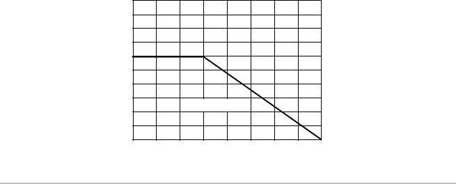
Figure 1. Derating Curve
http://onsemi.com
2

EMC2DXV5T1, EMC3DXV5T1, EMC4DXV5T1, EMC5DXV5T1
ELECTRICAL CHARACTERISTICS (TA = 25°C unless otherwise noted)
Characteristic |
Symbol |
Min |
Typ |
Max |
Unit |
|
|
|
|
|
|
|
|
Q1 TRANSISTOR: PNP |
|
|
|
|
|
|
OFF CHARACTERISTICS |
|
|
|
|
|
|
|
|
|
|
|
|
|
Collector-Base Cutoff Current (VCB = 50 V, IE = 0) |
ICBO |
− |
− |
100 |
nAdc |
|
Collector-Emitter Cutoff Current (VCB = 50 V, IB = 0) |
ICEO |
− |
− |
500 |
nAdc |
|
Emitter-Base Cutoff Current |
EMC2DXV5T1 |
IEBO |
− |
− |
0.2 |
mAdc |
(VEB = 6.0, IC = 5.0 mA) |
EMC3DXV5T1 |
|
− |
− |
0.5 |
|
|
EMC4DXV5T1 |
|
− |
− |
0.2 |
|
|
EMC5DXV5T1 |
|
− |
− |
1.0 |
|
|
|
|
|
|
|
|
ON CHARACTERISTICS |
|
|
|
|
|
|
|
|
|
|
|
|
|
Collector-Base Breakdown Voltage (IC = 10 mA, IE = 0) |
V(BR)CBO |
50 |
− |
− |
Vdc |
|
Collector-Emitter Breakdown Voltage (IC = 2.0 mA, IB = 0) |
V(BR)CEO |
50 |
− |
− |
Vdc |
|
DC Current Gain |
EMC2DXV5T1 |
hFE |
60 |
100 |
− |
|
(VCE = 10 V, IC = 5.0 mA) |
EMC3DXV5T1 |
|
35 |
60 |
− |
|
|
EMC4DXV5T1 |
|
80 |
140 |
− |
|
|
EMC5DXV5T1 |
|
20 |
35 |
− |
|
|
|
|
|
|
|
|
Collector−Emitter Saturation Voltage (IC = 10 mA, IB = 0.3 mA) |
VCE(SAT) |
− |
− |
0.25 |
Vdc |
|
Output Voltage (on) (VCC = 5.0 V, VB = 2.5 V, RL = 1.0 kW) |
VOL |
− |
− |
0.2 |
Vdc |
|
Output Voltage (off) (VCC = 5.0 V, VB = 0.5 V, RL = 1.0 kW) |
VOH |
4.9 |
− |
− |
Vdc |
|
Input Resistor |
EMC2DXV5T1 |
R1 |
15.4 |
22 |
28.6 |
kW |
|
EMC3DXV5T1, EMC4DXV5T1 |
|
7.0 |
10 |
13 |
|
|
EMC5DXV5T1 |
|
3.3 |
4.7 |
6.1 |
|
|
|
|
|
|
|
|
Resistor Ratio |
EMC2DXV5T1 |
R1/R2 |
0.8 |
1.0 |
1.2 |
|
|
EMC3DXV5T1 |
|
0.8 |
1.0 |
1.2 |
|
|
EMC4DXV5T1 |
|
0.17 |
0.21 |
0.25 |
|
|
EMC5DXV5T1 |
|
0.38 |
0.47 |
0.56 |
|
|
|
|
|
|
|
|
Q2 TRANSISTOR: NPN |
|
|
|
|
|
|
OFF CHARACTERISTICS |
|
|
|
|
|
|
|
|
|
|
|
|
|
Collector-Base Cutoff Current (VCB = 50 V, IE = 0) |
ICBO |
− |
− |
100 |
nAdc |
|
Collector-Emitter Cutoff Current (VCB = 50 V, IB = 0) |
ICEO |
− |
− |
500 |
nAdc |
|
Emitter-Base Cutoff Current |
EMC2DXV5T1 |
IEBO |
− |
− |
0.2 |
mAdc |
(VEB = 6.0, IC = 5.0 mA) |
EMC3DXV5T1 |
|
− |
− |
0.5 |
|
|
EMC4DXV5T1, EMC5DXV5T1 |
|
− |
− |
0.1 |
|
|
|
|
|
|
|
|
ON CHARACTERISTICS |
|
|
|
|
|
|
|
|
|
|
|
|
|
Collector-Base Breakdown Voltage (IC = 10 mA, IE = 0) |
V(BR)CBO |
50 |
− |
− |
Vdc |
|
Collector-Emitter Breakdown Voltage (IC = 2.0 mA, IB = 0) |
V(BR)CEO |
50 |
− |
− |
Vdc |
|
DC Current Gain |
EMC2DXV5T1 |
hFE |
60 |
100 |
− |
|
(VCE = 10 V, IC = 5.0 mA) |
EMC3DXV5T1 |
|
35 |
60 |
− |
|
|
EMC4DXV5T1, EMC5DXV5T1 |
|
80 |
140 |
− |
|
|
|
|
|
|
|
|
Collector−Emitter Saturation Voltage (IC = 10 mA, IB = 0.3 mA) |
VCE(SAT) |
− |
− |
0.25 |
Vdc |
|
Output Voltage (on) (VCC = 5.0 V, VB = 2.5 V, RL = 1.0 kW) |
VOL |
− |
− |
0.2 |
Vdc |
|
Output Voltage (off) (VCC = 5.0 V, VB = 0.5 V, RL = 1.0 kW) |
VOH |
4.9 |
− |
− |
Vdc |
|
Input Resistor |
EMC2DXV5T1 |
R1 |
15.4 |
22 |
28.6 |
kW |
|
EMC3DXV5T1 |
|
7.0 |
10 |
13 |
|
|
EMC4DXV5T1, EMC5DXV5T1 |
|
33 |
47 |
61 |
|
|
|
|
|
|
|
|
Resistor Ratio |
EMC2DXV5T1 |
R1/R2 |
0.8 |
1.0 |
1.2 |
|
|
EMC3DXV5T1 |
|
0.8 |
1.0 |
1.2 |
|
|
EMC4DXV5T1, EMC5DXV5T1 |
|
0.8 |
1.0 |
1.2 |
|
|
|
|
|
|
|
|
http://onsemi.com
3

EMC2DXV5T1, EMC3DXV5T1, EMC4DXV5T1, EMC5DXV5T1
TYPICAL ELECTRICAL CHARACTERISTICS − EMC2DXV5T1 PNP TRANSISTOR
(V) |
10 |
|
|
|
|
VOLTAGE |
|
|
|
||
|
IC/IB = 10 |
|
|
||
|
|
|
|
||
SATURATION |
1 |
|
|
25°C |
|
|
TA = −25°C |
|
|
||
EMITTER |
|
|
|
75°C |
|
0.1 |
|
|
|
||
COLLECTOR |
|
|
|
||
0.01 |
|
|
|
||
, |
0 |
20 |
40 |
50 |
|
CE(sat) |
|||||
|
IC, COLLECTOR CURRENT (mA) |
|
|
||
|
|
|
|
||
V |
|
Figure 2. VCE(sat) versus IC |
|
|
|
|
|
|
|
|
4 |
|
|
|
|
|
|
|
|
|
|
|
|
|
|
|
|
|
|
|
|
|
|
|
|
|
|
|
|
|
|
|
|
|
|
|
|
|
|
|
|
|
|
|
|
|
|
|
|
|
|
|
|
|
f = 1 MHz |
|
|
||
|
|
|
|
|
|
|
|
|
|
|
|
|||
|
|
|
|
|
|
|
|
|
|
lE = 0 mA |
|
|
||
(pF) |
3 |
|
|
|
|
|
|
|
|
TA = 25°C |
|
|
||
|
|
|
|
|
|
|
|
|
|
|||||
|
|
|
|
|
|
|
|
|
|
|
|
|
|
|
|
|
|
|
|
|
|
|
|
|
|
|
|
|
|
CAPACITANCE, |
2 |
|
|
|
|
|
|
|
|
|
|
|
|
|
|
|
|
|
|
|
|
|
|
|
|
|
|
||
ob |
|
|
|
|
|
|
|
|
|
|
|
|
|
|
1 |
|
|
|
|
|
|
|
|
|
|
|
|
|
|
|
|
|
|
|
|
|
|
|
|
|
|
|
||
C |
|
|
|
|
|
|
|
|
|
|
|
|
|
|
|
0 |
|
|
|
|
|
|
|
|
|
|
|
|
|
|
|
|
|
|
|
|
|
|
|
|
|
|
|
|
|
|
|
|
|
|
|
|
|
|
|
|
|
|
|
|
0 |
10 |
20 |
30 |
40 |
|
50 |
|||||||
VR, REVERSE BIAS VOLTAGE (V)
Figure 4. Output Capacitance
|
1000 |
|
|
|
|
|
VCE = 10 V |
GAIN |
|
|
TA = 75°C |
, DC CURRENT |
|
|
|
|
|
25°C |
|
100 |
|
−25°C |
|
|
|
|
|
FE |
|
|
|
h |
|
|
|
|
10 |
|
|
|
1 |
10 |
100 |
IC, COLLECTOR CURRENT (mA)
Figure 3. DC Current Gain
|
100 |
|
|
|
25°C |
|
|
|
|
|
|
|
|
|
|
|
75°C |
|
|
|
|
|
|
||
(mA) |
|
|
|
|
|
TA = −25°C |
|
|
|
|
|
|
10 |
|
|
|
|
|
|
|
|
|
|
|
|
CURRENT |
1 |
|
|
|
|
|
|
|
|
|
|
|
|
|
|
|
|
|
|
|
|
|
|
|
|
, COLLECTOR |
0.1 |
|
|
|
|
|
|
|
|
|
|
|
|
|
|
|
|
|
|
|
|
|
|
|
|
C |
|
|
|
|
|
|
|
|
|
|
|
|
I |
0.01 |
|
|
|
|
|
|
|
|
|
|
|
|
|
|
|
|
|
|
|
|
|
VO = 5 V |
|
|
|
|
|
|
|
|
|
|
|
|
|
|
|
|
0.001 |
0 |
1 |
2 |
3 |
4 |
5 |
6 |
7 |
8 |
9 |
10 |
|
|
|
|
|
|
Vin, INPUT VOLTAGE (V) |
|
|
|
|
||
Figure 5. Output Current versus Input Voltage
|
100 |
|
VO = 0.2 V |
|
|
|
|
|
|
|
|
|
|
|
|
(VOLTS) |
|
|
|
TA = −25°C |
|
|
|
|
|
|
|
|
|
|
|
, INPUT VOLTAGE |
10 |
|
|
|
25°C |
|
|
|
|
|
75°C |
|
|
|
|
1 |
|
|
|
|
|
|
|
in |
|
|
|
|
|
|
|
|
|
|
|
|
|
|
|
V |
|
|
|
|
|
|
|
|
0.1 |
0 |
10 |
20 |
30 |
40 |
50 |
IC, COLLECTOR CURRENT (mA)
Figure 6. Input Voltage versus Output Current
http://onsemi.com
4
 Loading...