74FST3345
8−Bit Bus Switch
The ON Semiconductor 74FST3345 is an 8−bit, high performance
switch. The device is CMOS TTL compatible when operating between
4 and 5.5 Volts. The device exhibits extremely low RON and adds
nearly zero propagation delay. The device adds no noise or ground
bounce to the system.
The device consists of an 8−bit switch with two Output/Enable pins
(OE and OE
Features
• R
ON
• Less Than 0.25 ns−Max Delay Through Switch
• Nearly Zero Standby Current
• No Circuit Bounce
• Control Inputs are TTL/CMOS Compatible
• Pin−For−Pin Compatible with QS3345, FST3345, CBT3345
• All Popular Packages: QSOP−20, TSSOP−20, SOIC−20
• All Devices in Package TSSOP are Inherently Pb−Free*
).
4 Typical
OE
A
A
A
A
A
A
A
A
GND
1
2
0
3
1
4
2
5
3
6
4
7
5
8
6
9
7
10
20
19
18
17
16
15
14
13
12
11
V
OE
B
B
B
B
B
B
B
B
CC
0
1
2
3
4
5
6
7
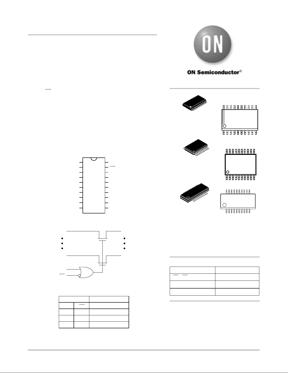
Figure 1. 20−Lead Pinout
20
20
20
QS SUFFIX
CASE 492A
http://onsemi.com
1
SOIC−20
DW SUFFIX
CASE 751D
1
TSSOP−20
DT SUFFIX
CASE 948E
1
QSOP−20
MARKING
DIAGRAMS
20
FST3345
AWLYYWW
1
20
FST
3345
ALYW
1
20
FST3345
AWLYWW
1
218
A
0
9
A
7
1
OE
19
OE
B
0
11
B
7
Figure 2. Logic Diagram
TRUTH TABLE
Inputs
OE
X
H
*For additional information on our Pb−Free strategy and soldering details, please
download the ON Semiconductor Soldering and Mounting Techniques
Reference Manual, SOLDERRM/D.
Semiconductor Components Industries, LLC, 2005
January, 2005 − Rev. 1
OE
L
X
L
H
Function
Connect
Connect
Disconnect
1 Publication Order Number:
A = Assembly Location
L, WL = Wafer Lot
Y = Year
W, WW = Work Week
PIN NAMES
Pin
OE1, OE
1A, 2A
1B, 2B Bus B
2
Description
Bus Switch Enables
Bus A
ORDERING INFORMATION
See detailed ordering and shipping information in the package
dimensions section on page 3 of this data sheet.
74FST3345/D

74FST3345
MAXIMUM RATINGS
Symbol Parameter Value Unit
V
V
V
I
I
OK
I
I
CC
I
GND
T
STG
T
T
MSL Moisture Sensitivity Level 1
F
V
ESD
I
Latchup
Maximum ratings are those values beyond which device damage can occur. Maximum ratings applied to the device are individual stress limit
values (not normal operating conditions) and are not valid simultaneously . If these limits are exceeded, device functional operation is not implied,
damage may occur and reliability may be affected.
1. Measured with minimum pad spacing on an FR4 board, using 10 mm−by−1 inch, 2−ounce copper trace with no air flow.
2. Tested to EIA/JESD22−A114−A.
3. Tested to EIA/JESD22−A115−A.
4. Tested to EIA/JESD78.
DC Supply Voltage 0.5 to 7.0 V
CC
DC Input Voltage 0.5 to 7.0 V
I
DC Output Voltage 0.5 to 7.0 V
O
DC Input Diode Current VI GND 50 mA
IK
DC Output Diode Current VO GND 50 mA
DC Output Sink Current 128 mA
O
DC Supply Current per Supply Pin 100 mA
DC Ground Current per Ground Pin 100 mA
Storage Temperature Range 65 to 150 C
Lead Temperature, 1 mm from Case for 10 Seconds 260 C
L
Junction Temperature Under Bias 150 C
J
Thermal Resistance (Note 1) SOIC
JA
TSSOP
QSOP
Flammability Rating Oxygen Index: 28 to 34 UL 94 V−0 @ 0.125 in
R
ESD Withstand Voltage Human Body Model (Note 2)
Machine Model (Note 3)
96
128
200
2000
200
Latchup Performance Above VCC and Below GND at 85C (Note 4) 500 mA
C/W
V
RECOMMENDED OPERATING CONDITIONS
Symbol Parameter Min Max Unit
V
V
V
T
t/V Input Transition Rise or Fall Rate Switch Control Input
5. Unused control inputs may not be left open. All control inputs must be tied to a high or low logic input voltage level.
Supply Voltage Operating, Data Retention Only 4.0 5.5 V
CC
Input Voltage (Note ) 0 5.5 V
I
Output Voltage (HIGH or LOW State) 0 V
O
Operating Free−Air Temperature 40 85 C
A
0
Switch I/O
0
CC
5
DC
V
ns/V
http://onsemi.com
2

74FST3345
†
DC ELECTRICAL CHARACTERISTICS
V
CC
Symbol Parameter Conditions (V) Min Typ* Max Unit
V
Clamp Diode Resistance IIN = 18mA 4.5 1.2 V
IK
V
High−Level Input Voltage 4.0 to 5.5 2.0 V
IH
V
Low−Level Input Voltage 4.0 to 5.5 0.8 V
IL
I
Input Leakage Current 0 VIN 5.5 V 5.5 1.0 A
I
I
OFF−STATE Leakage Current 0 A, B V
OZ
R
Switch On Resistance (Note 6) VIN = 0 V, IIN = 64 mA 4.5 4 7
ON
CC
5.5 1.0 A
VIN = 0 V, IIN = 30 mA 4.5 4 7
VIN = 2.4 V, IIN = 15 mA 4.5 8 15
VIN = 2.4 V, IIN = 15 mA 4.0 11 20
I
Quiescent Supply Current VIN = VCC or GND, I
CC
I
Increase In ICC per Input One input at 3.4 V, Other inputs at VCC or GND 5.5 2.5 mA
CC
= 0 5.5 3 A
OUT
*Typical values are at VCC = 5.0 V and TA = 25C.
6. Measured by the voltage drop between A and B pins at the indicated current through the switch.
AC ELECTRICAL CHARACTERISTICS
VCC = 4.5 to 5.5 V VCC = 4.0 V
Symbol Parameter Conditions Figures Min Max Min Max Unit
t
,
PHL
t
t
PZH
t
t
PHZ
t
Prop Delay Bus to Bus
(Note 7)
PLH
,
Output Enable Time VI = 7 V for t
PZL
,
Output Disable Time VI = 7 V for t
PLZ
7. This parameter is guaranteed by design but is not tested. The bus switch contributes no propagation delay other than the RC delay of the
typical On resistance of the switch and the 50 pF load capacitance, when driven by an ideal voltage source (zero output impedance).
VI = OPEN 3 and 4 0.25 0.25 ns
VI = OPEN for t
VI = OPEN for t
PZL
PLZ
PZH
PHZ
3 and 4 1.5 6.5 7.0 ns
3 and 4 1.0 8.0 8.2 ns
TA = 40C to 85C
Limits
TA = 40C to 85C
CAPACITANCE (Note 8)
Symbol Parameter Conditions Typ Max Unit
C
C
Control Pin Input Capacitance VCC = 5.0 V 3 pF
IN
Input/Output Capacitance VCC, OE = 5.0 V 5 pF
I/O
8. TA = 25C, f = 1 MHz, Capacitance is characterized but not tested.
ORDERING INFORMATION
Device Order Number Package Shipping
74FST3345DW SOIC−20 38 Units / Rail
74FST3345DWR2 SOIC−20 1000 Units / Tape & Reel
74FST3345DT TSSOP−20*
75 Units / Rail
(Pb−Free)
74FST3345DTR2 TSSOP−20*
2500 Units / Tape & Reel
(Pb−Free)
74FST3345QS QSOP−20 55 Units / Rail
74FST3345QSR QSOP−20 2500 Units / Tape & Reel
†For information on tape and reel specifications, including part orientation and tape sizes, please refer to our Tape and Reel Packaging
Specifications Brochure, BRD8011/D.
*This package is inherently Pb−Free.
http://onsemi.com
3
 Loading...