

Onkyo TXSR-501 Service Manual
SERVICE MANUAL
SERVICE MANUAL
Page 1
AV RECEIVER
TX-SR501/E
Ref. No. 3772
062003
MODEL
TX-SR501/E
Black, Golden and Silver models
BMDD,BMDC
BMPP,SMPP,BMPA,GMPA
BMWT,GMWT,GMWR,GMWQ
GMGK
120V AC, 60Hz
230-240V AC, 50Hz
120/220-230V AC, 50/60Hz
220V AC, 50Hz
SAFETY-RELATED COMPONENT
WARNING!!
COMPONENTS IDENTIFIED BY MARK ON THE
SCHEMATIC DIAGRAM AND IN THE PARTS LIST ARE
CRITICAL FOR RISK OF FIRE AND ELECTRIC SHOCK.
REPLACE THESE COMPONENTS WITH ONKYO
PARTS WHOSE PART NUMBERS APPEAR AS SHOWN
IN THIS MANUAL.
MAKE LEAKAGE-CURRENT OR RESISTANCE
MEASUREMENTS TO DETERMINE THAT EXPOSED
PARTS ARE ACCEPTABLY INSULATED FROM THE
SUPPLY CIRCUIT BEFORE RETURNING THE
APPLIANCE TO THE CUSTOMER.

Specifications
Page 2
TX-SR501/E
AMPLIFIER SECTION
Continuous Average Power output (FTC)
All channels: 65 watts per channel min. RMS at
Continuous Power output (DIN)
Maximum Power output (EIAJ)
Dynamic power output:
Total Harmonic Distortion: 0.08% at rated power
IM Distortion: 0.08% at rated power
Damping Factor: 60 at 8 Ω
Input Sensitivity and Impedance
DIGITAL INPUT (OPTICAL 1, 2): 0.5 Vp-p, 75 Ω
DIGITAL INPUT (COAXIAL): 0.5 Vp-p, 75 Ω
LINE (CD, VIDEO 1, 2, 3, TAPE): 200 mV, 47 kΩ
Multichannel Input
(DVD FRONT L/C/R, SURR L/R): 200 mV, 47 kΩ
(SUBWOOFER): 36 mV, 47 kΩ
Output Level and Impedance
Rec out (TAPE, VIDEO 1): 200 mV, 470 Ω
Pre out (SUBWOOFER): 1 V, 470 Ω
Frequency Response: 10 Hz to 100 kHz,
Tone Control
Bass: ±12 dB at 50 Hz
Treble: ±12 dB at 20 kHz
Signal-to-Noise Ratio: CD/TAPE: 100 dB
Muting: –50 dB
8 Ω, 2 channels driven from 20 Hz
to 20 kHz with no more than 0.08%
total harmonic distortion.
80 watts per channel min. RMS at
6 Ω, 2 channels driven from 1 kHz
with no more than 0.1% total harmonic distortion.
× 2 at 6 Ω
85 watts
115 watts
160 watts
125 watts
85 watts
0.08% at 1 watt output
0.08% at 1 watt output
+1/–3 dB (Direct mode)
(IHF-A, Direct mode)
× 2 at 6 Ω
× 2 at 3 Ω
× 2 at 4 Ω
× 2 at 8 Ω
VIDEO SECTION
Input Sensitivity and Impedance
VIDEO (DVD, VIDEO 1, 2, 3): 1 Vp-p, 75 Ω
S VIDEO (DVD, VIDEO 1, 2, 3): 1 Vp-p, 75 Ω (Y)
COMPONENT VIDEO 1, 2: 1 Vp-p, 75 Ω (Y)
Output Level and Impedance
VIDEO (VIDEO 1, 2, MONITOR): 1 Vp-p, 75 Ω
S VIDEO (VIDEO 1, 2, MONITOR): 1 Vp-p, 75 Ω (Y)
COMPONENT VIDEO OUT: 1 Vp-p, 75 Ω (Y)
0.28 Vp-p, 75 Ω (C)
0.7 Vp-p, 75 Ω (P
0.28 Vp-p, 75 Ω (C)
0.7 Vp-p, 75 Ω (P
B
B
, PR)
, PR)
TUNER SECTION
FM
Tuning Range
North American models: 87.50-108.00 MHz (100 kHz steps)
Other models: 87.50-108.00 MHz (50 kHz steps)
Usable Sensitivity
Mono: 11.2 dBf, 1.0 µV (75 Ω, IHF)
Stereo: 17.2 dBf, 2.0 µV (75 Ω, IHF)
50 dB Quieting Sensitivity
Mono: 17.2 dBf, 2.0 µV (75 Ω)
Stereo: 37.2 dBf, 20.0 µV (75 Ω)
Capture Ratio: 2.0 dB
Image Rejection Ratio
North American models: 40 dB
Other models: 85 dB
IF Rejection Ratio: 90 dB
Signal-to-Noise Ratio
Mono: 76 dB
Stereo: 70 dB
Alternate Channel Attenuation: 55 dB
Selectivity: 50 dB (DIN)
AM Suppression Ratio: 50 dB
Total Harmonic Distortion
Mono: 0.2%
Stereo: 0.3%
Frequency Response: 30 Hz-15 kHz, –1.0 dB
Stereo Separation: 45 dB at 1 kHz
0.9 µV (75 Ω, DIN)
23 µV (75 Ω DIN)
30 dB at 100 Hz-10 kHz
AM
Tuning Range
North American models: 530-1,710 kHz (10 kHz steps)
European & Australian models: 522-1,611 kHz (9 kHz steps)
Worldwide models: 522-1,611 kHz (9 kHz steps), or
Usable Sensitivity: 30 µV
Image Rejection Ratio: 40 dB
IF Rejection Ratio: 40 dB
Signal-to-Noise Ratio: 40 dB
Total Harmonic Distortion: 0.7%
530-1,710 kHz (10 kHz steps)
GENERAL
Power Supply and Power Consumption:
AC 120 V, 60 Hz 4.6 A
AC 230-240 V, 50 Hz 370 W
AC 220-230 V and 120 V switchable, 50/60 Hz 370 W
Dimensions (W
Weight
North American models: 19.6 lbs., 8.9 kg
European models: 21.6 lbs., 9.8 kg
Other models: 21.8 lbs., 9.9 kg
× H × D): 17-1/8" × 5-7/8" × 14-13/16"
× 150 × 376 mm
435
REMOTE CONTROL
Transmitter: Infrared
Signal range: Approx. 16 ft., 5 meters
Power supply:
Two “AA” batteries (1.5 V
× 2)
Specifications and features are subject to change without notice. Power supply and voltage vary depending on the area in which the unit is purchased.
SERVICE PROCEDURES
Page 3
TX-SR501/E
1. Replacing the fuses
This symbol located near the fuses indicates that the
fuse used is fast operating type. For continued protection against
fire hazard, replace with same type fuse. For fuse rating refer to
the marking adjacent to the symbol.
Ce symbole indique que le fusible utlise est a rapide.
Pour une protection permanente, n'untiliser que fusibles de
meme type. Ce darnier est la qu le present symbol est
appse.
CIRCUIT NO. PART NO.
DESCRIPTION
F6901,F6902 252198 or 8A-UL or
252261 8A-T/UL-ST2 <D>
252099 8A-EAK ,Fuse <O>
F901 252166 or 6.3A-UL/T-237 or
252260 6.3A-T/UL-ST2,Fuse <D/T/Q/R>
F902 252076, 3.15A-SE-EAK,
252242 or 3.15A-SE-TL250V or
252276 3.15A-SE-TL250V <O>
F903 252075, 2.5A-SE-EAK,
252241 or 2.5A-SE-TL250V or
252275 2.5A-SE-TL250V,Fuse <O>
Note: <D>:120V model only
<O>: Other models except 120V model
<T>: Asian model only for 230V
<R>: Chinese model only
<Q>: Hongkong model only
2. To initialize the unit
This device employs a microprocessor to perform various
functions and operations. If interference generated by an external
power supply, radio wave, or other electrical source results in
accident which causes the specified operations and functions to
operate abnormally.
To perform a result, please follow the procedure below.
1.Press and hold down the VIDEO-1 button, then press the
STANDBY/ON button.
2.After "CLEAR" is displayed, the preset memory and each
mode stored in the memory, such as surround, are
initialized and will return to the factory setting.
3. Unplug the power supply cord.
3. Safety-check out
(U.S.A. model only)
After correcting the original service problem, perform the
following safety check before releasing the set to the customer.
Leakage Current Check
Measure leakage current to a known earth ground(water pipe,
conduit, etc.) by connecting a leakage current tester between
the earth ground and exposed metal parts of the appliance
(input/output terminals, screwheads,metal overlays, etc.).
Plug the power supply cord directly into a 120V AC 60 Hz outlet
and turn Standby switch on. Any current meausred must not
exceed 0.5mA.
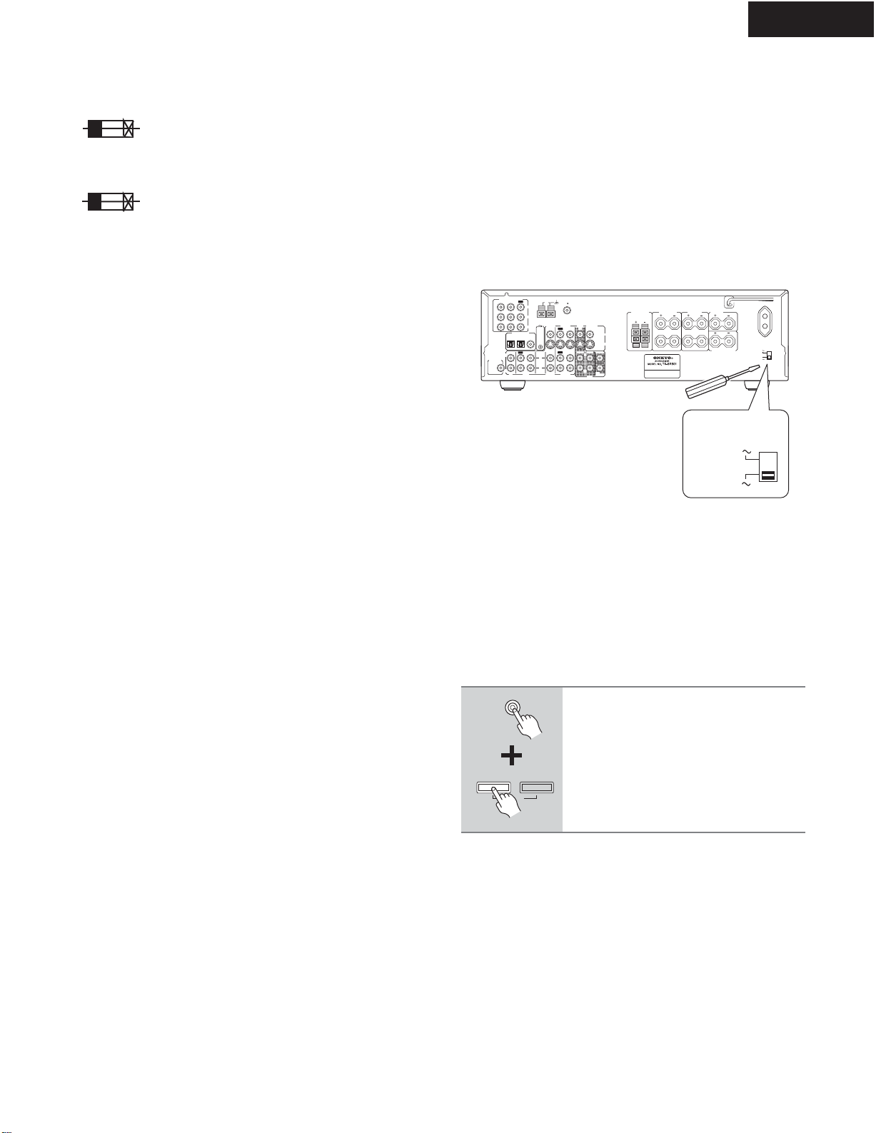
4.Setting the voltage selector (Worldwide models
only)
Worldwide models are equipped with a voltage selector to conform
with local power supplies. Be sure to set this switch to match the
voltage of the power supply in your area before plugging in the unit.
Determine the proper voltage for your area: 220-230 V or 120 V. If
the preset voltage is not correct for your area, insert a screwdriver
into the groove in the switch. Slide the switch all the way to the
upper (120 V) or to the lower (220-230 V), whichever is appropriate.
COMPONENT VIDEO
ANTENNA
FM
AM
75
Y
B
P
VIDEO 1
VIDEO 2
PR
12
IN
TAPE
DVD MONITOR
OUT
IN
IN
IN
OUT
REMOTE
CONTROL
OUT
IN
IN
SURR
FRONT
L
R
L
R
VIDEO 1
VIDEO 2
DVD
FRONT
SPEAKERS B
L
VIDEO
R
S VIDEO
CENTER
SUB
OOFER
W
L
R
FRONT
SPEAKERS A
SURROUND
SPEAKERS
L
R
CENTER
SPEAKER
SURROUND BACK
SPEAKER
AC OUTLET
SWITCHED
100W MAX.
VOLTAGE
SELECTOR
120 V
220-230 V
VOLTAGE
SELECTOR
120 V
220-230 V
SUBWOOFER
PRE OUT
VIDEO 1
/2/3
DVD IN
OUT
IN
DIGITAL INPUT
OPTICAL COAXIAL
OUT
IN
L
R
CD
5.Setting the AM tuning step frequency
(Worldwide models only)
If you are using the Worldwide model (i.e., your TX-SR501/
TX-SR501E has a VOLTAGE SELECTOR on the rear
panel), you need to set the AM tuning interval for compatibility with AM broadcasts in your particular country. The initial setting is 9 kHz.
North America: 10 kHz
Other countries: 9 kHz
TUNER
T o set the AM tuning interval, while
holding down the [TUNER] button,
press the [MEMORY] button.
MEMORY
FM MODE
CLEAR
Note:
All presets are deleted when you change this setting.
Controls & Connectors—Continued
Page 4
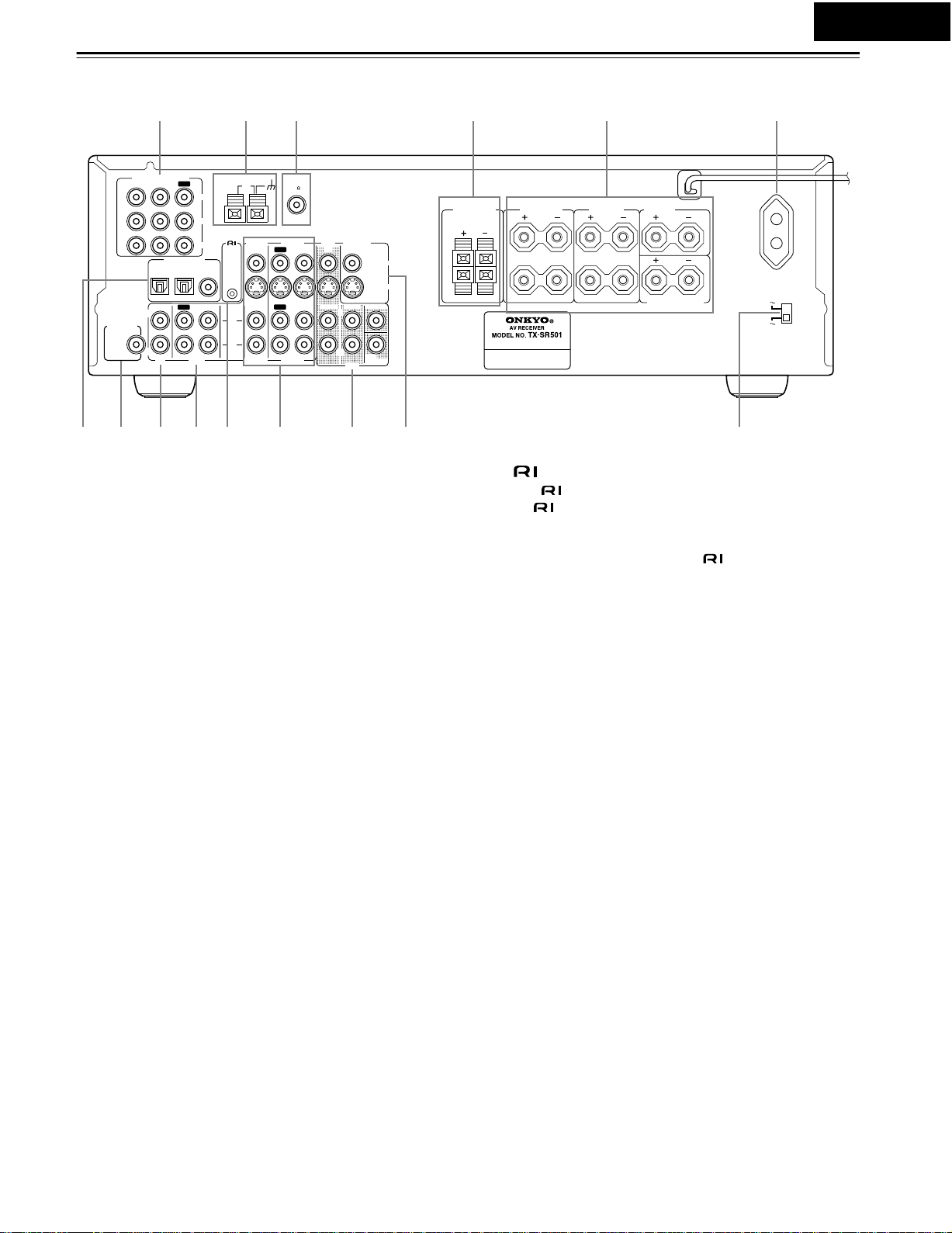
Rear Panel
TX-SR501/E
1 6
COMPONENT VIDEO
VIDEO 1
/2/3
DVD IN
IN
DIGITAL INPUT
OPTICAL COAXIAL
IN
L
SUBWOOFER
PRE OUT
R
CD
789JK M N O
ANTENNA
OUT
12
OUT
TAPE
AM
Y
P
B
PR
REMOTE
CONTROL
IN
L
R
VIDEO 2
IN
IN
VIDEO 2
OUT
OUT
FM
75
VIDEO 1
VIDEO 1
IN
IN
DVD MONITOR
OUT
IN
SURR
FRONT
L
R
DVD
CENTER
SUB
WOOFER
VIDEO
S VIDEO
L
4532
FRONT
SPEAKERS B
L
R
FRONT
SPEAKERS A
L
R
L
R
SURROUND
SPEAKERS
CENTER
SPEAKER
SURROUND BACK
SPEAKER
AC OUTLET
SWITCHED
100W MAX.
VOLTAGE
SELECTOR
220-230 V
K (19)
A COMPONENT VIDEO (10, 12, 14, 16)
These RCA/phono connectors can be used to connect a TV,
DVD player, or other AV component with component video
inputs and outputs.
B AM ANTENNA (22, 23)
These push terminals are for connecting an AM antenna.
C FM ANTENNA (22, 23)
This connector is for connecting an FM antenna.
D FRONT SPEAKERS B (21)
These push terminals are for connecting speaker set B.
E FRONT SPEAKERS A, SURROUND SPEAKERS,
CENTER SPEAKER & SURROUND BACK
SPEAKER (21)
These terminal posts are for connecting speaker set A, including the front, surround, center, and surround-back speakers.
They accept bare wires or banana plugs (European models
don’t accept banana plugs).
F AC OUTLET (11)
This switched AC outlet can be used to supply power to
another AV component. The connector type depends on the
country in which you purchased your TX-SR501/
TX-SR501E.
G DIGITAL INPUT OPTICAL 1, 2 & COAXIAL (10,
13, 14, 16–18)
These optical and coaxial connectors can be used to connect a
CD, DVD, or LD (laser disc) player, or other AV component
with digital outputs.
This (Remote Interactive) connector can be connected to
the connector on another Onkyo AV component, for
example, a CD player, DVD player, or cassette recorder. The
TX-SR501/TX-SR501E’s remote controller can then be used
to control that component. To use , you must make an analog RCA/phono connection between your TX-SR501/
TX-SR501E and the other AV component, even if they are
connected digitally.
L VIDEO 1 IN/OUT & VIDEO 2 IN (10, 14–16, 39)
These connectors can be used to connect a VCR or other AV
component. There are RCA/phono connectors for connecting
to stereo analog audio inputs and outputs, and S-Video and
composite video (RCA/phono) connectors for connecting to
video inputs and outputs.
M DVD IN/MULTI CH INPUT (10, 12, 13)
The FRONT, SURR, CENTER, and SUBWOOFER RCA/
phono connectors can be used to connect AV components with
multiple analog audio outputs, including DVD players with
individual 5.1 surround analog outputs. There’s an S-Video
input and composite video (RCA/phono) input for connecting
the video signal.
N MONITOR OUT (10, 12)
These S-Video and composite video (RCA/phono) outputs can
be connected to the video input on your TV or projector.
O VOLTAGE SELECTOR (Worldwide model only)
(5)
This voltage selector provides compatibility with power systems around the world.
H SUBWOOFER PRE OUT (21)
This RCA/phono connector can be used to connect an active
subwoofer.
I CD IN (10, 17)
These RCA/phono connectors can be used to connect a CD
player with analog outputs.
J TAPE IN/OUT (10, 17, 18)
These RCA/phono connectors can be used to connect a cassette recorder, MiniDisc recorder, or other recorder with analog inputs and outputs.
Tip:
A turntable with a built-in preamp can be connected to a pair of
unused TX-SR501/TX-SR501E analog inputs. To connect a
turntable without a built-in preamp, you’ll need a commercially available phono preamp. See pages 17 and 18 and the
instructions supplied with your phono preamp and turntable for
more information.
120 V
Worldwide
model only
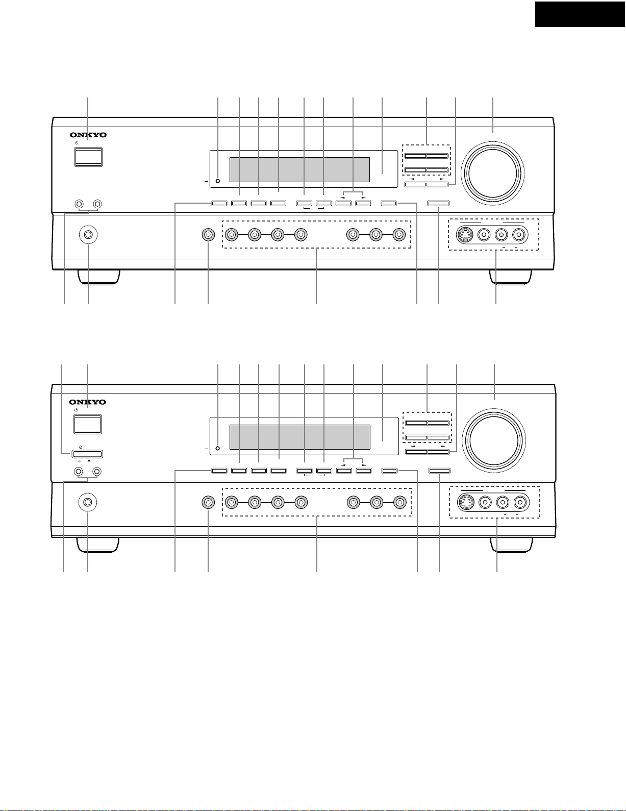
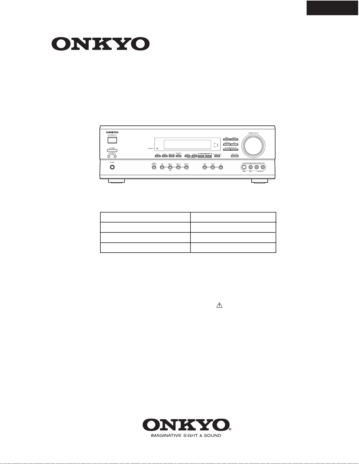
Front Panel
Page 5
North American Model
234589JKML6N7
TX-SR501/E
STANDBY/ON
AB
SPEAKERS
PHONES
OQR TUSP
Other Models
234589JKML6N7
1
STANDBY/ON
POWER
OFFON
AB
SPEAKERS
PHONES
STANDBY
STANDBY
AUDIO
SELECTOR
AUDIO
SELECTOR
DISPLAY
DISPLAY
MASTER VOLUME
STEREO
DIRECT
DSP
SURROUND
PRESET/ADJUST
DIGITAL INPUT
VIDEO 1
VCR
DIGITAL INPUT
VIDEO 1
SUBWOOFER
MODE
VIDEO
SUBWOOFER
MODE
VIDEO
FM MODE
MEMORY
CLEAR
2
3
VIDEO
FM MODE
MEMORY
CLEAR
VIDEO
2
3
DIMMER
DVD
DIMMER
DVD
TUNING
TAPE TUNER
TUNING
TAPE TUNER
SPEAKER ADJUST
SPEAKER ADJUST
AUDIO ADJUST
INPUT
C
D
STEREO
DIRECT
DSP
SURROUND
PRESET/ADJUST
AUDIO ADJUST
C
D
VIDEO 3
VIDEO L R
S VIDEO AUDIO
MASTER VOLUME
INPUT
VIDEO 3
OQR TUSP
A POWER switch (24)
The North American model doesn’t have this switch.
This is the main power switch. When set to OFF, the
TX-SR501/TX-SR501E is completely shutdown. When set to
ON, the TX-SR501/TX-SR501E is in Standby mode and the
STANDBY indicator lights up.
Don’t turn on the power until you’ve completed, and double
ked all connections.
chec
Note:
Turning on the TX-SR501/TX-SR501E may cause a momentary power surge that might interfere with other electrical
equipment on the same circuit. If this is a problem, plug the
TX-SR501/TX-SR501E into a different branch circuit.
VCR
VIDEO L R
S VIDEO AUDIO
B STANDBY/ON button (24)
This button is used to set the TX-SR501/TX-SR501E to On or
Standby. For models with a POWER switch, this button has no
effect unless the POWER switch is set to ON.
C STANDBY indicator (24)
This indicator lights up when the TX-SR501/TX-SR501E is in
Standby mode, and it flashes while a signal is being received
from the remote controller.
D DIMMER button (32)
This button is used to adjust the display brightness.
E DIGITAL INPUT button (24)
This button is used to assign the digital inputs.
F SUBWOOFER MODE button (25)
This button is used to select the Subwoofer modes.
Controls & Connectors—Continued
Page 6
TX-SR501/E
G MEMORY button (30, 31)
This button is used when storing and deleting radio presets.
H FM MODE button (31)
This button is used to select the FM radio Stereo and Mono
modes. It’s also used when deleting radio presets.
I TUNING [ ] [ ] buttons (30)
These buttons are used to tune into radio stations.
J Remote control sensor (5)
This sensor receives control signals from the remote controller.
K Listening mode buttons (36)
These buttons are used to select the listening modes.
L PRESET/ADJUST [ ] [ ] buttons (25, 26, 31,
37)
This button is used to select radio presets and adjust parameter
values.
M MASTER VOLUME control (28, 30)
This control is used to set the volume of the TX-SR501/
TX-SR501E.
N SPEAKER A & B buttons (28, 32)
These buttons are used to turn speaker sets A and B on and off.
O PHONES jack (33)
This 1/4-inch phone jack is for connecting a standard pair of
stereo headphones for private listening.
P DISPLAY button (32)
This button is used to display various information about the
currently selected source.
Q AUDIO SELECTOR button (28, 29)
This button is used to select the input signal format.
R Input selector buttons (24, 28–30, 39)
These buttons are used to select the audio and video sources:
CD, DVD, TAPE, TUNER, VIDEO 1, VIDEO 2, or VIDEO 3.
S SPEAKER ADJUST button (25, 26)
This button is used to adjust various speaker-related parameters.
T AUDIO ADJUST button (37)
This button is used to set the Bass, Treble, Late Night, Cinema
Filter, Center Image, Panorama, Dimension, and Center Width
functions.
U VIDEO 3 INPUT connectors (15, 39)
These S-Video, composite video (RCA/phono), and analog
audio (RCA/phono) inputs can be used to connect a video
camera or games console.
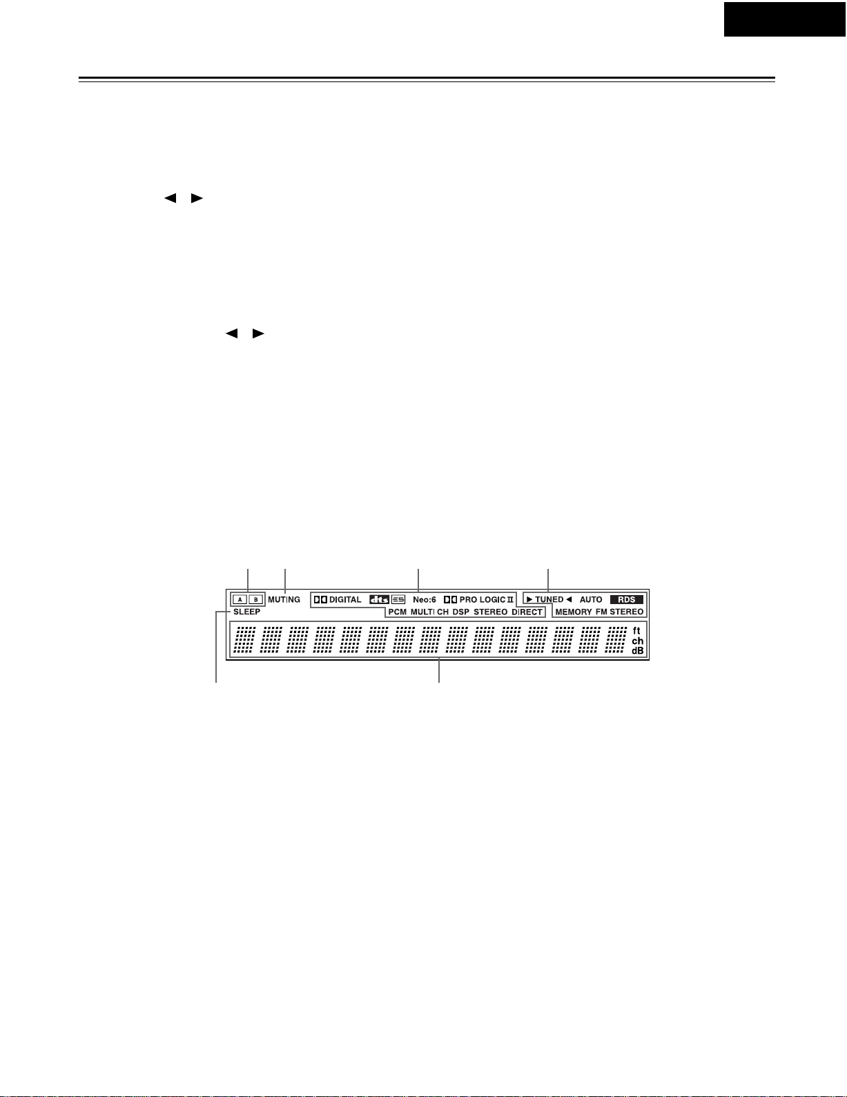
Display
12 3 4
56
For detailed information, refer to the pages in parenthesis.
1 A & B speaker indicators (28, 32)
Indicator A lights up when speaker set A is on. Indicator B
lights up when speaker set B is on.
2 MUTING indicator (33)
This indicator flashes when the TX-SR501/TX-SR501E is
muted.
3 Source/listening mode indicators (28, 36)
These indicators display information about the currently
selected source and listening mode.
4 Tuning indicators (30, 31)
TUNED (30): This indicator lights up when the TX-SR501/
TX-SR501E is tuned into a radio station.
AUTO (30): This indicator lights up when the Auto Tuning
function is on.
RDS (European model only) (31): This indicator lights
up when the TX-SR501E is tuned into a radio station that supports RDS (Radio Data System).
MEMORY (31): This indicator lights up when programming
radio presets.
FM STEREO (31): This indicator lights up when the
TX-SR501/TX-SR501E is tuned into a stereo FM station.
5 SLEEP indicator (33)
This indicator lights up when the Sleep function has been set.
6 Message area
This area of the display shows various information about the
currently selected source.
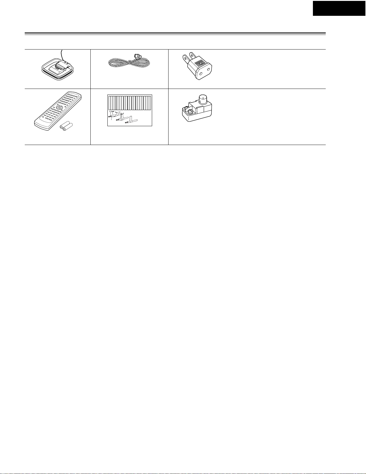
Supplied Accessories
Page 7
Make sure you have the following accessories:
Indoor FM antenna
(connector type varies from
AM loop antenna
country to country)
Power-plug adapter
TX-SR501/E
Only supplied in certain countries. Use
this adapter if your AC outlet does not
match with the plug on the TX-SR501/
TX-SR501E’s power cord. (Adapter varies from country to country.)
Left
Left
Left
Left
Left
Left
Right
Right
Surround
Surround
Surround
Surround
Surround
Right
Surround
Left
Surround
Right
Surround
Left
3
Right
Right
Right
Right
Center
Center
Zone 2
Zone 2
Zone 2
Zone 2
Surround Back
Surround Back
Surround Back
Surround Back
Zone 2
Right
Zone 2
Left
Center
Zone 2
Right
Zone 2
Left
Surround Back
Right
Surround Back
Left
Center
Surround Back
Right
Surround Back
Left
Not supplied with North American and
European models.
75/300-ohm antenna
adapter
Remote controller &
two batteries (AA/R6)
Left
Left
Left
Left
Front
Front
Front
Front
Right
Right
Right
Right
Zone 2
Zone 2
Zone 2
Zone 2
/
/
/
/
SP-B
SP-B
SP-B
SP-B
Zone 2
Zone 2
Zone 2
Zone 2
/
/
/
/
Front
Left
Front
Right
SP-B
Left
SP-B
Right
Front
Left
Front
Right
SP-B
Left
SP-B
Right
1
2
Speaker Cable
Speaker cable labels
* In catalogs and on packaging, the letter added to the end of the product name indicates the color of the TX-SR501/TX-SR501E. Specifications and operation
are the same regardless of color.
Controls & Connectors—Continued
Page 8
TX-SR501/E
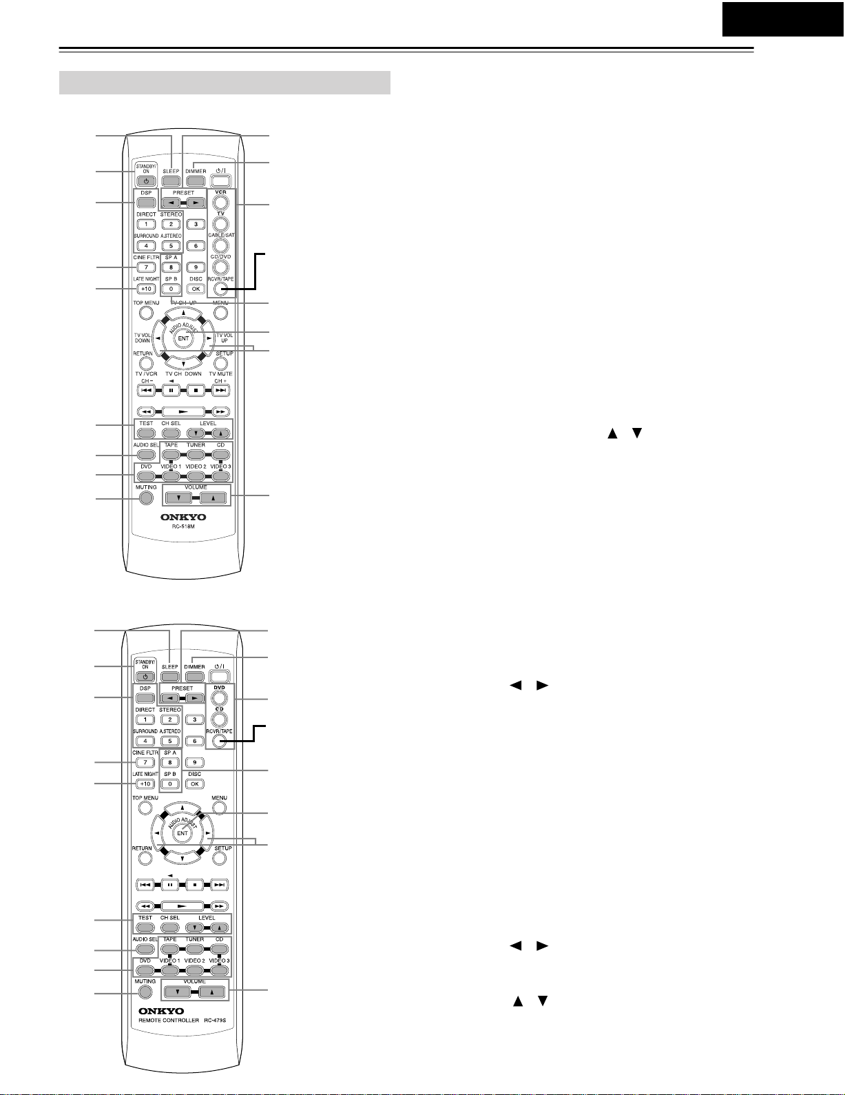
Remote Controller—RCVR Mode
RC-518M (North American model)
1J
2
3
4
K
L
Press this to select
RCVR mode
5
M
N
O
6
7
8
9
RC-479S (other models)
P
1J
2
3
4
K
L
Press this to select
RCVR mode
M
5
N
O
6
7
8
9
P
This page describes only those buttons that can be used to
control the TX-SR501/TX-SR501E when the remote controller is in RCVR mode (Rece
To select RCVR mode, press the [RCVR] button.
iver mode).
A SLEEP button (33)
This button is used to set the Sleep function. This function can
be set only with the remote controller.
B STANDBY/ON button (24)
This button is used to set the TX-SR501/TX-SR501E to On or
Standby.
C Listening mode buttons (36)
These buttons are used to select the listening modes.
D CINE FLTR button (37)
This button is used to set the Cinema Filter function.
E LATE NIGHT button (37)
This button is used to set the Late Night function.
F TEST, CH SEL & LEVEL [ ] [ ] buttons (27, 29,
33)
These buttons are used to set the level of each speaker individually. This function can be set only with the remote controller.
G AUDIO SEL button (29)
This button is used to select analog or digital inputs for the
CD, DVD, TAPE, VIDEO 1, VIDEO 2, and VIDEO 3 sources.
H Input selector buttons (28, 30, 39)
These buttons are used to select the audio and video sources:
CD, DVD, TAPE, TUNER, VIDEO 1, VIDEO 2, and
VIDEO 3.
I MUTING button (33)
This button is used to mute the TX-SR501/TX-SR501E. This
function can be set only with the remote controller.
J PRESET [ ] [ ] buttons (31)
These buttons are used to select radio presets.
K DIMMER button (32)
This button is used to adjust the display brightness.
L Remote Controller Mode buttons (28, 40, 42)
These buttons are used to select the remote controller modes.
To select RCVR mode, press the [RCVR] button.
M SP A & SP B buttons (28, 32)
These buttons are used to turn on and off speaker sets A and B
individually.
N AUDIO ADJUST button (37)
This button is used to set the Bass, Treble, Late Night, Cinema
Filter, Center Image, Panorama, Dimension, and Center Width
functions.
O ADJUST [ ] [ ] buttons (37)
These buttons are used to adjust the functions selected with
the AUDIO ADJUST button.
P VOLUME [ ] [ ] buttons (27, 28, 33)
These buttons are used to set the volume of the TX-SR501/
TX-SR501E.
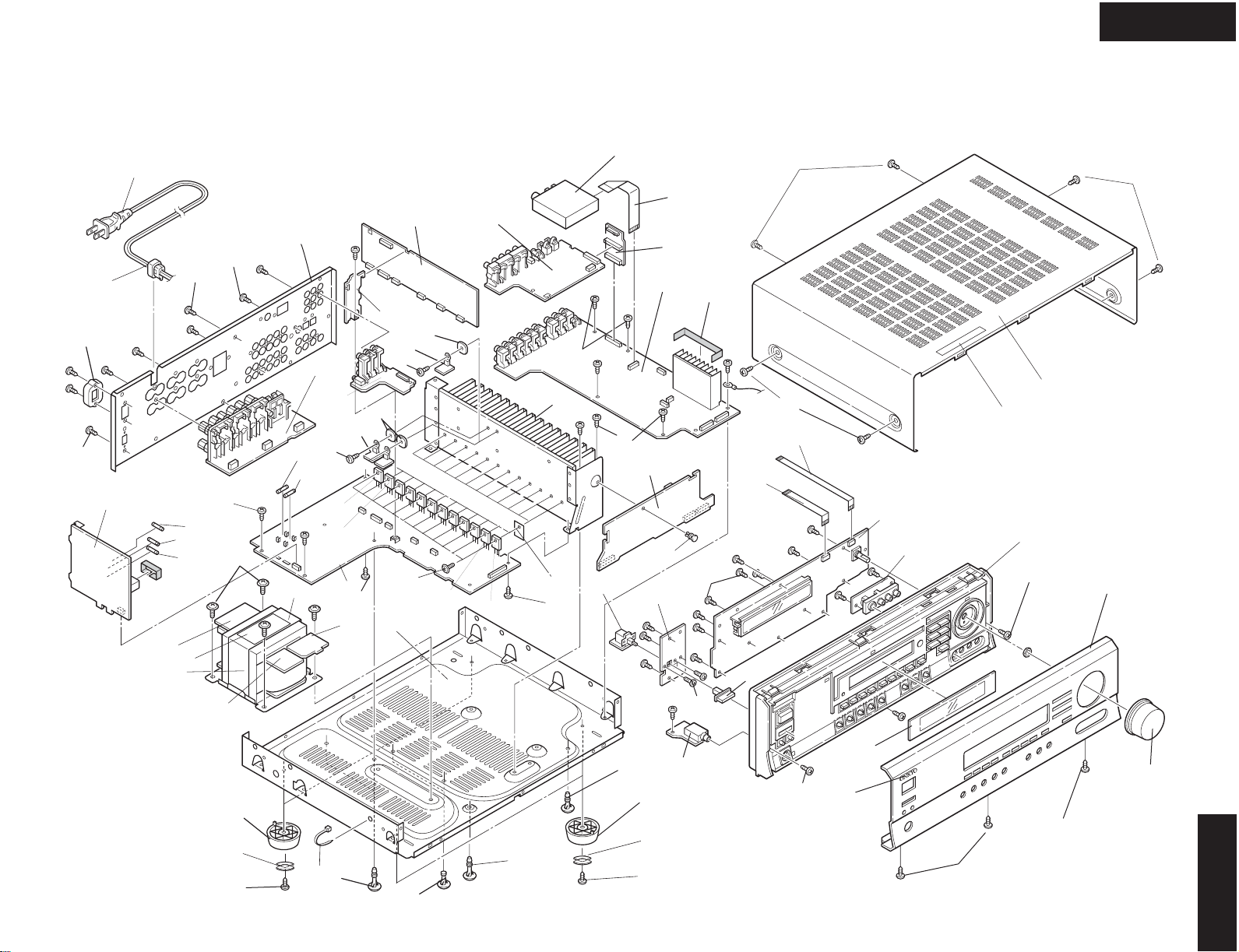
EXPLODED VIEW
Page 9
TX-SR501/E
11
Chinese
model only
32
33
U24
P901
U23
T901
33
F903
F901
F902
63
U25
33
2
U31
P101
U9
31
U15
U27
**
U28
U27
2
2
13
Q6055
5
U14
U10
**
U28
2
F6901
F6902
Q6050
Q6060
9
9
U21
U13
U26
Q6065
55
2
12
U17
U1
54
2
2
U22
U12
10
*
U4
P7503
2
4
3
*
P7502
*
17
17
U3
U6
17
16
18
1
2
51
21
22
23
56
52
25
53
53
24
TX-SR501/E
6
8
8
7
U5
21
22
* 3, 4 & U22:Except 120V model
** U27X2:Except 120V model
23
2
TX-SR501/E
Y
Page 10
A
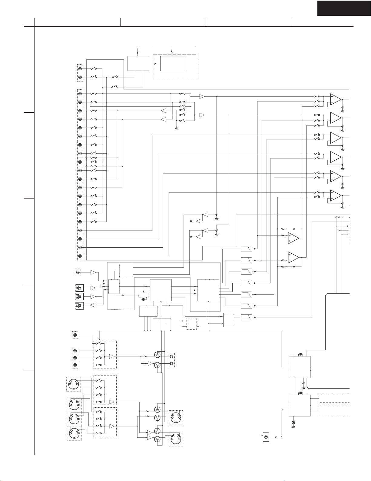
BLOCK DIAGRAM
1
VIDEO3
CD
TAPE OUT
TAPE IN
VIDEO-3
2
VIDEO-2 IN
VIDEO-1 OUT
VIDEO-1 IN
DVD
MLS/MRS
3
C/SW
COAXIAL
OPTICAL 1
OPTICAL 2
OPTICAL OUT
4
VIDEO3
COMPOSITE VIDEO INPUT
VIDEO2
VIDEO1
DVD
VIDEO 3
S-VIDEO INPUT
VIDEO 2
5
VIDEO 1
DVD
BD3811K1
80
79 78
2
1
72
71
4
3
6
5
73
8
74
7
76
75
S
10
9
12
S
11
14
13
16
15
CTLA/B
VIDEO SW
YC
YC
YC
YC
LA7956
AK4586
LA7956
6dB
6dB
6dB
77
(1/2)
AK4586
2CH A/D
96/24
DIR
LA7956
FM/AM
TUNER
PACK
OSC
12.288MHZ
MX27L2000
MX27L4000
FLASH ROM
BCD
Main microprocessor
RDS
DECODER
BU1923F
European model only
INPUT GAIN
INPUT GAIN
INPUT GAIN
INPUT GAIN
INPUT GAIN
BACK UP
INPUT GAIN
0/6dB
0/6dB
0/6dB
0/6dB
0/6dB
0/6dB
SELCL
SELMUT
SELDA
KEY
FL DISPLA
69
66
43
40
30
33
CS493292
A17
A16
A15
0dB
0dB
0dB
1
1
18
NC
-1
20
NC
-1
17
19
AK4586
DSP
M5M5V1080KV
UPD441000LGU
1M SRAM
+2.5V
DSP
ROM/RAM
RST.CS.INTREQ/CL/DA/SCDO
MEMORY
VMUT1
VMUT2
COMPOSITE VIDEO OUT
+3.3V
+5V
MONITOR OUT
VIDEO 1
S-VIDEO OUTPUT
Y
C
Y
C
MONITOR OUT
VIDEO 1
1
1
1
1
L
96/24
6CH D/A
AK4586
RST.CS/CL/DA/CDTO/INT1.2.
-6dB
INPUT ATT
50KLPF
50KLPF
R
50KLPF
SL
50KLPF
SR
50KLPF
C
50KLPF
SW
50KLPF
SB
AK4384
2CH D/A
REMOTE
SENSOR
2321262528
27
OPAMP
10.5dB
OPAMP
12.5MHZ
MAIN MICRO
PROCESSOR
78K/4
UPD7842
25AGC
SUB MICRO
PROCESSOR
78K/0
UPD780232
GC-8BT
STANDBY
24
22
5MHZ
TX-SR501/E
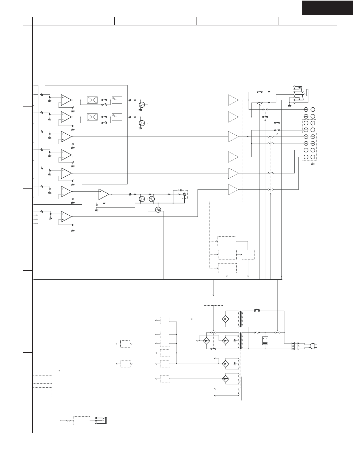
Page 11
A
BLOCK DIAGRAM
1
VOLUME
MASTER
0~-103dB
OUTPUT GAIN
68
OUTPUT GAIN
65
OUTPUT GAIN
OUTPUT GAIN
39
OUTPUT GAIN
31
OUTPUT GAIN
34
0~18dB
OPAMP
OUTPUT GAIN
0~18dB
OPAMP
OPAMP
2
69
66
43 42
40
30
33
0~18dB
OPAMP
0~18dB
OPAMP
0~18dB
OPAMP
0~18dB
OPAMP
36
BASS/TREBLE
BASS/TREBLE
15dB
BASSBOOST
38
37
35
Q305
OPAMP
BCD
Power Amplifier
55
57
+27dB
+27dB
+27dB
+27dB
+27dB
SWPO
+27dB
AMUT
HEADPHONE
L
R
SPBL
SPBR
SL
SR
C
SB
BD3812
3
VOLTAGE
SENSOR
CURRENT
SENSOR
VOLTAGE
SENSOR
VOLH
SEC1H
SEC1H
CONTROL
4
AUDIO
AUDIO
+7V
-7V
STANDBY
+12V
-12V
-VP
VIDEO
AF/TU
AF
+5.6V
-27V
+12V
+12V
-12V
+B1
SEC1H
RELAY
RELAY
+B2
+B1H
+B1L
T902
SEC1
SEC2
PROTE
CTION
PRO
PRI
T901
FUSE
SPHP
SPF
SPCS
HPMUT
POWER SW
POWER
RELAY
AC OUTLET
SPB
HPDET
POWER
AC IN
SEC3
DSP/TU
+5V
FLAC
AY
5
To FL TUBE
FLAC
RI INTER
FACE
RI
TX-SR501/E
100K
Page 12
A
SCHEMATIC DIAGRAM 1
NADIS-7403
U3
1
2
D7502
UDZ5.1B
R7505
220K
3
F2F2NPNPP35
59
Q7504
KRA103S
D7503
1SS352
56
57
58
P34
55
54
R7532
BCD
Display and video sections
P33
P32
P31
P30
P29
P28
P27
P26
P25
P24
P23
P22
P21
P20
P19
P18
P17
P16
P15
P14
P13
33
34
35
36
37
38
39
40
41
42
43
44
45
46
47
48
49
50
51
52
53
41
42
43
P46/FIP3840
R7504
10K
SYSOUT
47K
R7506
4.7K
R7507
4.7K
C7507
104Z
22
21
P47/FIP3939
P50/FIP4038
P51/FIP4137
P52/FIP4236
P53/FIP4335
P54/FIP4434
P55/FIP4533
P56/FIP4632
P57/FIP4731
P60/FIP4830
P61/FIP4929
P62/FIP5028
P63/FIP5127
P64/FIP5226
VDD025
AVDD24
VSS023
ANI220
4.7K
R7508
22:ANI0
21:ANI1
ANI319
AVSS18
4.7K
R7509
P41/FIP3345
P42/FIP3444
41:P45/FIP37
42:P44/FIP36
43:P43/FIP35
P01/INTP116
P02/TI17
1K
1K
10K
R7512
R7511
R7510
P34/FIP2850
P35/FIP2949
P36/FIP3048
P37/FIP3147
P40/FIP3246
Q7502
UPD780232GC
-030-8BT
P20/SCK314
P21/SO313
P2212
P2311
POO/INTP015
10K
10K
10K
10K
R7514
R7515
R7516
R7513
Q7501 HNA-16MM39T
P12
P11
P10P9P8P7P6P5P4P3P2P116G
26
27
28
29
30
31
32
FIP21 57
FIP22 56
FIP23 55
61:FIP19
P31/FIP2553
P32/FIP2652
P33/FIP2751
P24/BUSY10
IC5
P25SO19
P26/SI18
P27/SCK17 P30/FIP2454
X2
RESET
4
6
22
23
24
25
60
VLOAD
VDD259
FIP20 58
FIP18 62
FIP17 63
FIP16 64
FIP15 65
FIP14 66
FIP13 67
FIP12 68
FIP11 69
FIP10 70
FIP9 71
FIP8 72
FIP7 73
FIP6 74
FIP5 75
FIP4 76
FIP3 77
FIP2 78
FIP1 79
FIP0
VSS12
X13
1
VDD1
X7501
CST5.00MGW
21
61
80
15G
14G
13G
12G
11G
10G9G8G7G6G5G4G3G2G1GNPNPF1
10
11
12
13
14
15
16
17
18
19
20
10K
R7503
2SC2712
Q7503
KTC3875
F1
123456789
100K
2.7K
2.7K
R7521
C7510 102J
C7509 102J
220
R7531
D7505
STANDBY
Q7506
RN1402
KRC102S
VIDEO3
102J
C7511
R7522
10K
R7527
S7625
2.7K
R7523
10K
R7526
K2
VIDEO2
K3
S7624
102J
2.7K
R7520
C7508
U7501
SPS4441E1
100/6.3
C7514
102J
C7517
104Z
C7516
4
S7616
SP A
R7615
1.2K
S7501
S7615
SP B
R7614
820
NASW-7404
U4
S7614
STANDBY
R7613
560
104Z
C7515
JL7501B
SYSIN
JL7501A
GND
KEY0
R7626
S7627
FM
K0
K1
2.2K R7621 330R7625 1.2K R7624 820 R7623 560 R7622 470
S7626
MODE
IRF
STBYLED
VIDEO1
R7518
1K
560
VAJ
VBJ
R7517
R7528
SBMDI
SBMLDY
R7612 470 R7611330
S7613
DIM
MER
DVD
S7623
5
S7637
S7647
TUNI
NG<
R7646 2.2K
AUDIO
ADJUST
S7636
S7646
TUNI
PRE
NG<
SET>
S7635
S7645
MEMO
RY
PRE
SET<
S7634
S7644
TAPE
DSP
S7633
S7643
TUNER
SURRO
UND
1K
1K
560
R7529
R7524
R7530
SBMDO
SBMCLK
SBMRST
S7612
SW
S7622
AUDIO
R7631
CD
S7632
R7641 330R7645 1.2K R7644 820 R7643 560 R7642 470
S7642
STE
101J
C7522
MODE
SEL
330R7632 470R7633 560R7634 820R7635 1.2KR7636 2.2K
REO
102J
C7523
S7611
S7621
S7631
S7641
C7513
INPUT
DIGITAL
DIS
PLAY
SP
DIRECT
104Z
K0K1K2
ADJUST
K3
SYSIN
HPDET
SBMDI
SBMDO
SBMCLK
SBMLDY
TO NADG-7401
L7505
-VP
SBMRST
P7502A
220K
NCH1477
R7519
TX-SR501/E
2G
6
L7505
-VP
Page 13
A
U17
U3
1
1GNPNPF1F11
234
5
104Z
C7501
C7502
33/50
104Z
C7503
R7501
473Z
C7504
C7505
R7502
220
220
UDZ8.2B
D7501
473Z
NAETC-7838
RI
A
B
VMUT2
VMUT1
OPT2
DGND
TO NADG-7821
OPT1
+5V
COAX
104Z
C7506
OPTOUT
+12V
CNPT
P801B
BCD
PRINTED CIRCUIT BOARD VIEW 1-2
NASW-7404,Standby switch PC board
U4
TO NAVD-7831
SPA SPB
JL7501B
0
2
2
STANDBY
S7616 S7615
2
S7614
25137404
NCSW-7404
2
Component side
GND
GND
P206A
P243A
TO NAVD-7847
2
R7614
R7613
R7615
Soldering side
U6
3
NAETC-7406,Front video PC board
P253BP261B
P251
P254
P251
NCETC-7406
25137406
1
Component side
GND
GND
V4C
V4Y
R253
RL
R262
471J<O>
V4
R251
330
101J<D>
V4L
V4R
GND
R262
4
100K
R7519
D7507
1SS352
C7521
220/6.3
220K
NCH1477
L7504
220K
NCH1477
5
JL7502A
GND
FAC2
FAC1
HPL
HPR
HPE
+5.6S
GND
P7502A
P7503A
TO NAETC-7410
HPDET
GND
HPL
HPE
HPR
C7518
JL7502B
E7501
102J
C7519
102J
U5
C7520
102J
P7501
HEADPHONE
NAETC-7405
C262
C263
C253
Soldering side
NAETC-7406
R261
C261
S
YC
R253
P253B
P251
R252 75R251 75
75
C253
104Z
P254
U6
VIDEO3 IN
V
R261
471J<O>
C263
104Z
P261B
R252
330
C261
C262
101J<D>
TX-SR501/E
A
Page 14
A
BCD
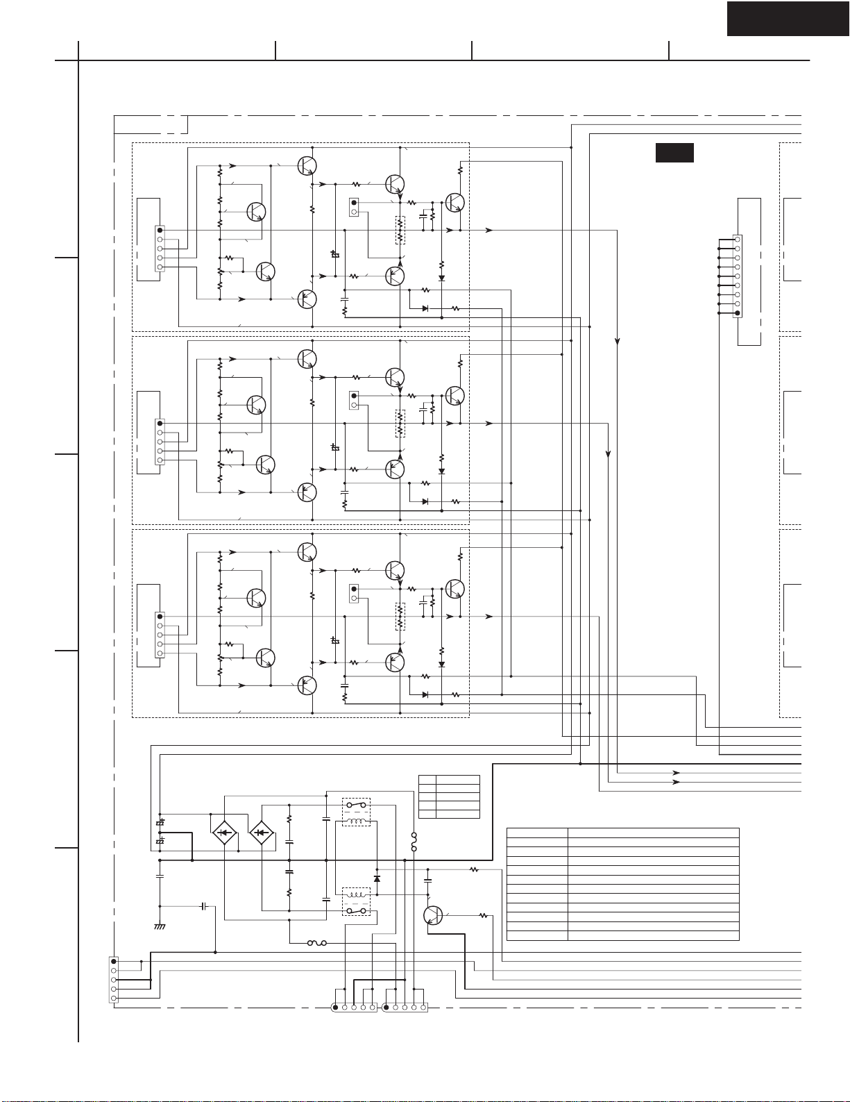
SCHEMATIC DIAGRAM 4 Driver amplifier
NAAF-7830
1
U9
SL
R5093
C5013
R5003
1K
C5003
2
101K
R5043
D5003
MTZJ5.6B
22/16
R5013
56K
2.2K
R5103
100K
-0.1V
R5023
330
82K
-43.0V
C5023
10/50
Q5003
R5063
1.2K
R5113
1K
-0.7V
Q5013
R5053
4.7K
Q5053
-43.6V
R5073
560
R5083
3.3K
C5103
10/63
C5043
220/16
[100/16]
section
47.1V
C5073
0V
R5133
18K
C5093
-47.1V
C5113
10/63
120
101J
1.1V
C5083
040D
R5173
(1/4W)
R5163
120
(1/4W)
47.7V
Q5033
C5053
47/50
R5033
56K
-1.1V
Q5043
-47.7V
R5183
10
(1/4W)
48.5V
NF
-B1
+B1
B+
B-
R5193
10
(1/4W)
-48.5V
P6003A
(SCH-4)
TO NAAF-7842
P406
SR
R5094
C5014
R5004
3
1K
C5004
101K
R5044 2.2K
D5004
MTZJ5.6B
SB
22/16
R5014
56K
R5104
100K
-0.1V
R5024
330
R5095
4
C5015
R5005
1K
C5005
101K
R5045
D5005
MTZJ5.6B
22/16
R5015
56K
2.2K
R5105
100K
-0.1V
R5025
330
82K
-43.0V
C5024
10/50
82K
-43.0V
C5025
10/50
Q5004
Q5005
R5064
1.2K
R5065
1.2K
R5114
1K
-0.7V
R5115
1K
-0.7V
R5054
4.7K
Q5054
-43.6V
R5074
560
R5055
4.7K
Q5055
-43.6V
R5075
560
Q5014
Q5015
R5084
3.3K
R5085
3.3K
C5104
10/63
C5044
220/16
C5105
10/63
C5045
220/16
0V
R5134
18K
C5114
10/63
0V
R5135
18K
C5115
10/63
47.1V
C5074
-47.1V
47.1V
C5075
-47.1V
C5094
101J
120
C5095
101J
120
1.1V
C5084
040D
R5174
(1/4W)
1.1V
C5085
040D
R5175
(1/4W)
R5164
120
(1/4W)
47.7V
Q5034
C5054
47/50
R5034
56K
-1.1V
Q5044
-47.7V
R5165
120
(1/4W)
47.7V
Q5035
C5055
47/50
R5035
56K
-1.1V
Q5045
-47.7V
R5184
10
(1/4W)
R5185
10
(1/4W)
48.5V
NF
-B1
+B1
R5194
10
(1/4W)
-48.5V
48.5V
NF
-B1
+B1
R5195
10
(1/4W)
-48.5V
P6004A
B+
B-
P6005A
B+
B-
(SCH-4)
TO NAAF-7842
(SCH-4)
TO NAAF-7842
5
SEMICONDUCTORS
NO.
Q5000-05,5010-15 KTC3200-BL OR 2SC1775A-E,F OR 2SC1845-E
Q5030-35 KTA1024-Y,O OR 2SA949-Y,O
Q5040-45 KTC3206-Y,O OR 2SC2229-Y,O
Q5050-55 KTC3199-GR,2SC1740S-R,S,2SC2458-GR
TX-SR501/E
Page 15
A
BCD
SCHEMATIC DIAGRAM 4 Driver amplifier
TO NADG-7821
1
P406A
E
ESBECESLESRERE
2
3
(SCH-2)
E
E
E
E
E
E
(SCH-4)
E
TO NAAF-7842
E
E
E
P6011A
P306A
L
L
R5090
82K
C5010
R5000
1K
C5000
101K
R5040
D5000
MTZJ5.6B
R
R5001
1K
C5001
101K
R5041 2.2K
D5001
MTZJ5.6B
22/16
C5011
22/16
R5010
56K
2.2K
R5100
100K
R5011
56K
R5101
100K
-0.1V
R5020
330
-43.0V
C5020
10/50
R5091
82K
-0.1V
R5021
330
-43.0V
C5021
10/50
R5060
Q5001
R5061
1.2K
1.2K
R5110
1K
-0.7V
R5111
1K
-0.7V
R5050
4.7K
Q5050
-43.6V
R5070
560
R5051
4.7K
Q5051
-43.6V
R5071
560
Q5010Q5000
Q5011
section
C5100
10/63
C5040
220/16
R5130
R5080
3.3K
C5101
10/63
C5041
220/16
R5131
R5081
3.3K
0V
18K
C5110
10/63
0V
18K
C5111
10/63
47.1V
C5070
-47.1V
47.1V
C5071
-47.1V
C5090
101J
R5170
120
C5091
101J
R5171
120
1.1V
C5080
040D
(1/4W)
1.1V
C5081
040D
(1/4W)
R5160
120
47.7V
Q5030
C5050
47/50
R5030
56K
-1.1V
Q5040
-47.7V
R5161
120
47.7V
Q5031
C5051
47/50
R5031
56K
-1.1V
Q5041
-47.7V
(1/4W)
(1/4W)
R5180
10
(1/4W)
R5181
10
(1/4W)
48.5V
NF
-B1
+B1
R5190
10
(1/4W)
-48.5V
NF
-B1
+B1
R5191
10
(1/4W)
-48.5V
P6000A
B+
B-
48.5V
P6001A
B+
B-
(SCH-4)
TO NAAF-7842
(SCH-4)
TO NAAF-7842
U9
C
R5092
4
C5012
R5002
1K
C5002
101K
R5042
D5002
MTZJ5.6B
22/16
R5012
56K
2.2K
R5102
100K
-0.1V
R5022
82K
330
-43.0V
C5022
10/50
Q5002
R5062
1.2K
R5112
1K
-0.7V
R5052
4.7K
Q5052
-43.6V
R5072
560
Q5012
R5082
3.3K
C5102
10/63
C5042
220/16
0V
R5132
18K
C5112
10/63
47.1V
C5072
-47.1V
C5092
101J
120
1.1V
C5082
040D
R5172
(1/4W)
R5162
120
47.7V
Q5032
C5052
47/50
R5032
56K
-1.1V
Q5042
-47.7V
(1/4W)
R5182
10
(1/4W)
NF
-B1
+B1
R5192
10
(1/4W)
-48.5V
48.5V
P6002A
B+
B-
(SCH-4)
TO NAAF-7842
5
SEMICONDUCTORS
NO.
Q5000-05,5010-15 KTC3200-BL OR 2SC1775A-E,F OR 2SC1845-E
Q5030-35 KTA1024-Y,O OR 2SA949-Y,O
Q5040-45 KTC3206-Y,O OR 2SC2229-Y,O
Q5050-55
KTC3199-GR,2SC1740S-R,S,2SC2458-GR
TX-SR501/E
R
0
M
VP
Page 16
A
BCD
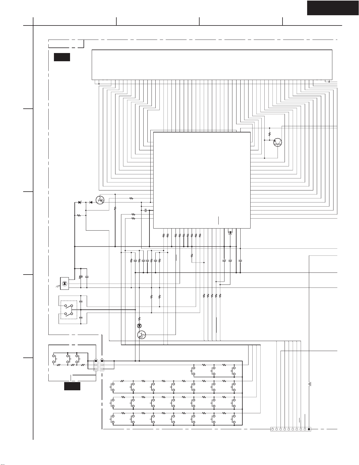
SCHEMATIC DIAGRAM 2 Digital and main microprocessor
R300
CD
330
330
R301
P301
R302
330
330
R303
R304
330
103Z
C308
330
R305
C322
104Z
C323
104Z
C310~C321:101J <120V>
471J <Other>
R310
330
330
R311
R312
330
330
R313
R314
330
330
C325
R315
R316
104Z
330
330
R317
R318
330
330
R319
R320
330
330
R321
C326
104Z
1
TAPE-1 OUT
TAPE-1 IN
VIDEO-2 IN
2
VIDEO-1 OUT
VIDEO-1 IN
P304
DVD
MLS/MRS
C/SW
P305
3
CDR
101K <120V>
471J <Other>
101K <120V>
471J <Other>
CDL
C301 C300C321
TOR -12VAF
101J
C302
101J
TOL
C303
TIR
101J <120V>
*
471J <Other>
C304
101J <120V>
*
471J <Other>
C305
C311 C310
101J
C312
101J
C313
*
C314
*
C315
*
C316
*
C317
*
C318
*
C319
*
C320
*
TIL
V2IR
V2IL
V1OR
V1OL
V1IR
V1IL
DVDR
DVDL
MSW
MC
47k
CDR
1
47k
CDL
2
47k
TIR
3
47k
TIL
4
47k
V3IR
5
47k
V3IL
6
47k
V2IR
7
47k
V2IL
8
47k
V1IR
9
47k
V1IL
10
47k
DVDR
11
47k
DVDL
12
47k
MRS
13
47k
MLS
14
47k
MSW
15
47k
MC
16
47k
ADCL
17
18
ADCR SELDA
19
20
47k
DAC_R
21
47k
DMIXR
22
47k
DAC_L
23
47k
DMIXL
24
NJM4565M
OR MPC4570
7
Q302
C327
C328
R362
10K
Q302
1
NJM4565M
OR MPC4570G2
V4R
80
47k
DAC_RS
8
R36110K
330J
330J
4
V4L
TUL
79
47k
47k
47k
DAC_LS
DAC_SW
5
6
2
3
78
272625
TUR
77
47k
47k
28
DAC_C
DAC_R
V1OL
V1OR
47k
297032
30
C334
10/16
DAC_L
R347
10K
R387
2.2K
R386
2.2K
R348
10K
TUL
TUR
31
R359
470
R360
470
TOL
C333
10/16
DAC_SW
TOR
71
7273747576
BD3811K1
33
34
Q301
35
OUT_C
C329
10/16
69
68
363738
OUT_LS
OUT_SW
P261A
C330
10/16
67
66
65
TREBLE
BAAS
BOOST BASS
VCC
VEE
MUT
CL
DA
LOGIC
40
39
C332
10/16
OUT_RS
OUT_SW
OUT_C
14
OUT1
OUT213
Q323BD3812F
IN1
AGND12
1
C335
332J
C336
64
332J
63
62
R363
C338
61
10K
563J
60
59
R364
58
C340
10K
563J
57
56
55
54
C347
53
100/16
52
51
50
C348
49
100/16
48
SELCK
47
46
45
44
43
42
41
C331
10/16
+7V
-7V
CL 8
DA 9
SEL 12
DGND11
MUTE10
AGND24
AGND36
IN23
VCC7
VEE
5
78L07
Q321
+7V
C359
C362
OUT_L
OUT_R
104Z
O
I
G
10/16
Q322
79L07
-7V
I
O
G
10/16
C367
SELMUT
C349
10/16
R367
1K
NADG-7821
sections
C366
+12VAF
C6404
10/16
104Z
C6406
10/16
79M12
+12VVD
C6410
78M12
10/16
Q6406
+5VDSP
78M05
C6412
10/16
C351
330J
2.2K
5.6K
R370
R369
47K
R383
10K
6
C350
221J
Q305
R368
5
8
+12VAF
NJM4565M
OR MPC4570
7
U1
Q6402
O
G
Q6403
O
G
Q6405
O
G
O
G
OUT_L
OUT_R
OUT_RS
OUT_C
I
78M12
I
I
C6409
223Z
I
C6411
223Z
R6402
10
C6403
1/2W
223Z
R6403
33
223Z
R6407 3.3
2.2
1/2W
47/16
47/16
C354
470
270
RN1441
R330
470
R331
470
R373
470
R374
R375
R389
470
R376
Q312
1/2W
1W
R384
220K
-22V
C9512
223Z
GND
+22V
1
GND
RN1441
Q307
RN1441
Q308
470
R388
100
Q313
RN1441
C360
474K
C6405
R6410
C353
C358
47/16
-12VAF
+12VAF
DAC_SB
Q305
C861
NJM4565M
OR MPC4570G2
102J
4
1
R857
12K
4
7
Q802
NJM4565M
NJM4565M
Q802
1
8
4
7
Q803
NJM4565M
NJM4565M
Q803
1
8
7
Q804
NJM4565M
NJM4565M
Q804
1
3
2
R858
C848
5
6
2
3
C849
C850
5
6
2
3
C851
C852
4
5
6
2
3
8
C853
C860
10/16
4
5
DAC
_C
DAC_
SW
DAC_LS
DAC_RS
DAC_L
DAC_R
GND
C854
10/16
C855
47/16
C856
10/16
C857
10/16
C858
10/16
C859
10/16
R854
8.2K
C862
152J
R848
153J
152J
R850
152J
152J
152J
15K
2.2K
2.2K
R849
2.2K
2.2K
R851
R852
2.2K
R853
2.2K
681J
C840
C841
C842
C843
C844
C845
821J
822J
821J
821J
821J
821J
R855
2.2K
R840
2.2K
R841
R842
2.2K
R843
2.2K
R844
2.2K
R845
2.2K
2.2K
R856
R832
R833
R834
R835
R836
R837
C863
10/16
22K
100K
100K
C834
10/16
100K
100K
C835
100K
100K
ADCL
ADCR
C832
10/16
C833
10/16
10/16
C836
10/16
C837
10/16
C820
C819
104Z
10/16
C821
104Z
C822
220/6.3
C807
104Z
C808
C809
10/16
C364
10/16
104Z
L806
NCH-1471
C806
C363
11
13
16
022M
P/S9
AOUTR10
AOUTL
DZFR15
DZFL
220/6.3
23
24
25
26
27
28
29
30
31
32
33
RIN
C810
10/16
VCOM12
VSS
VDD14
R826
10K
CDTI
8
CCLK 7
6
CSN
PDN
5
R825
LRCK 4
AK4384
R824
SDTI 3
R823
BICK 2
R822
Q805
MCLK 1
DSPDO
DIRCS
104Z
DSPSCK
D801
D802
C816
220
220
R814 220
R813
R812
AVDD
CSN
AVSS
DFZ2
CCLK
VCOM
23:VREFH
DFZ1
LOUT3
ROUT3
LOUT2
Q801
ROUT2
LOUT1
ROUT1
LIN
PVDD
SLAVE
RX4
PVSS
R
3435363738394041424344
18K
R815
47/16
C811
104Z
C800
330J
330J
C812
R816
330
R817
RX3
C818
102J
47
47
47
47
INT0[L]
CDTO/SCDO[L]
INT1[L]
47
1K
1K
220
R810
R809
R808
R811
CDTI
CDTO
INT1
INT0
AK4586
I2C
RX2
TST
RX3
330J
330J
C813
C814
R818
R819
330
330
RX1
+5VDSP
RX2
GND
R807
SDTI1
SDTI3
SDTO
BICK
LRCK
MCKO
TVDD
DVSS
DVDD
RX1
R820
330
DIRPD
1213141516171819202122
XTI
PDN
XTO
TX
47
GND
SDTI2
022M
L801
10K
104Z
C715
1
8
VCC
Q707
72
TC7WU04FU
63
GND4
5
R739 1M
X701 CSTCV12.2
+3.3V
CDA
SRDA
L804
022M
R806
102J
R801
L803
022M
L802
104Z
104Z
47
47
47
47
47
022M
R805
R804
R803
L805
BK1608LM182
C817
150J
C801
47/16
+5VDSP
TX
LRDA
SDTO
BCK
LRCK
MCK2
R821
X801
12.288M
HC-49/U03C
470
11
10
9
8
7
6
5
C805
4
C804
3
2
1
C815
L
DSPRST1[L]
TX-SR501/E
7
C
Page 17
A
SCHEMATIC DIAGRAM 2 Digital and main microprocessor
-VP
Q9501
2SA1015-GR
R9506
KTA1266-GR
-22V
1
C9512
223Z
GND
R9509
+22V
100K
D9508
UDZ27D
GND
C6401
104J
Q307 RN1441
R377
R378
RN1441
308
2
R379
R380
R381
R390
R388
100
R382
Q313
RN1441
C360
474K
Q306
3
NCH-1471
L704
104Z
715
022M
8
VCC
07
L706
7
U04FU
6
L705
5
BK1608
1M
LM182
CSTCV12.2MTJ0C4
C9511
223Z
22K
22K
22K
GND
22K
22K
22K
R385
100
22K
C365
222J
AMUT
RN2402
OR KRA102S
BK1608LM182
1/2W
R9508
15K
C9510
220/63
P6403
GND
RSPO
DSPMCK
22
R9507
1SR154-400
C9508
4700/16
P406
LPO
RPO
LSPO
CPO
SBO
C352
104Z
SWPO
GND
1SR154-400
15K
D9506
4
DSPMCK
C708
R718
33K
103K
CMPRE
Q/LRC
C709105K
LRCK
DSPRST1[L]
+2.5V
29 DATA017
LKN2
R719330
R72047
R7214.7K
C710
105K
471J
C711
C712
104Z
36
R722
1K
R723
4.7K
R7244.7K
39
R725
47
AUDA
C713
101J
TA2
NCH1471
L702
C716
022M
100/6.3
NCH-1471
L701
022M
5
C9507
D9507
220/35
C9505
2200/35
C9506
470/35
D9509
D9510
D9511
D9512
P306
P351
BCK
LRCK
SDTO
330
330
330
R717
R715
R716
28
27
CLKIN30
CLKSEL31
FILT232
CMPCLK/SCLKN2
FILT133
VDDA34
VSSA35
CMPDAT/RCV958/SDATAN2
RESET
DD37
AUDATA041
AUDATA1
40
47
47
R727
R726
R728
47
LRDA
D9502-9505:
RL1N4003
D9505
D9503
D9504
D9502
C9503
104J
10
R746
SDTO
BCK
330
C707
104Z
R714
VDD3 23
VSS3 24
SDTAN1 22
LRCKN1 26LRCLK42
Q701
CS493292-CL
SCLK43 SCLKN1/STCCLK2 25
VDD11
VSS12
MCLK44
47
47
R730
R729
104Z
C714
MCK2
220
R7067
DSPCS1[L]
INTREQ1
CDTO/SCDO[L]
R708220
R707
R706
220
EXTMEM
R709
47
47
10K
R712
R713
10K
20CS18
21
EXTMEM
DATA116
DATA215
DATA314
SCDIO/SCDOUT 19
ABOOT/_INTREQ
VSS213
VDD212
DATA411
DATA510
DATA6 9
DATA7 8DC38
A0/SCCLK 7
RD/R/_W
XMT9583
WR/DA4
5
6
R701
R702
47
330
R703
4.7K
SBDA
R749
R750
10
10
WE
C9502
104J
C9501
104J
A4 5
A5 6
A6 7
A7 8
A8 9
GND10
Q7002
TC74VHC541FT
Y316
Y415
Y514
Y613
Y712
Y8
11
220
220
220
220
220
220
R7070
R7072
R7069
R7073
R7074
R7068
A171[L]
A151[L]
A161[L]
FMEM/SRAM1[L]
+3.3V
R738
DSPCS1[L]
R737
R736
R735
220
R734
R733
R732
R731
10K
R710
R711
100/6.3
R757
R756
R755 10
R754
C703
R753
10
10
R751
10
10
A1/S
CDIN
J
1
0
10K
1
C701
R704
DSPCL[3.3V]
RD
DSPDA[3.3V]
R752
R748
A3 4
Y217
10K
10K
C706
R705
220
R7075
10K
10K
10K
10K
10K
10K
10
10
10
330
A2 3
Y118
104Z
A1 2
G2
19
BCD
TO TUNER PACK
P101
SD
TUR
TUL
GND
DET
+12VAF
R102
R103
22K
22K
STEREO
*
*
Q101
R105
680K
*
C105
104Z
*
European
RDSDET
model only
470J
C188
3.3K
R106
*
AMUT
SELMUT HPMUT
SELCK
SELDA
ADDR18
DIRCS
DSPCS
ROM/RAM 232TXD
A151 232RXD
A161
A171
DSPSCK
DSPDO
DSPRST
CDTO/SCDO
INT1
INT0
DIRPD
1/50
C7005
100/6.3
Q7001
D7004
D7002
R7033
1
G1
VCC20
L703
NCH-1479
470M
C7010
104Z
CDTO/SCDO
TC74HCT7007
OUTCTL1VCC
0D20Q19
1D31Q18
2D42Q17
3D53Q16
4D64Q15
5D75Q14
6D86Q13
7D97Q12
C101
TMUT
22K
R7839
R7141
10K
R7041
10K
R7042
220
R7043
220
R7044
R7045
R7046
R7047
R7048
220
R7049
1K
R7050
1K
R7051
1K
R7052
1K
R7053
220
R7054
220
R7055
220
R7056
1K
R7057
1K
R7058
1K
R7059
220
KRC104S
RN1404
C7004
C7006
1SS352
47K
220
R7083
Q7003
9
101112
220
220
INT0
INT1
R7082
R7081
INT1[L]
104Z
C720
Q704
TC74VHC574FT
+5VDSP
3.3/50
C103
22K
R7138
41
42
43
44
45
46
47
48
49
50
51
52
53
54
55
56
57
58
59
60
R7060
47K
104Z
104Z
C7007
220
R7085
12345678
13
14
220
R7084
INT0[L]
20
A0 A8
A1 A9
A2 A10
A3 A11
A4 A12
A5 A13
A6 A14
A7 A15
RD RD
CK 11GND10
P801
TX
RX1
RX2
GND
GND
PLLCL
PLLDA
FMSIG
PLLSTB
100K
101J
R104
C104
3.3/50
OR
RN1404
SD
PLLCL
PLLDA
TMUT
PLLSTB
KRC104S
STEREO
R7040
R7038
R7036
R7039
R7035
R7037
R7134
R7034
1K
470
220
220
220
220
2.2K
2.2K
40
Q7008
MPD784225GC222-8BT
61626364656667686970717273747576777879
R7063
R7064
R7065
POFF
R7062
R7066
1K
1K
1K
1K
C7008
220K
D7003
C7012
INTREQ1
47/16
CSTCV12.5MXJ
RDSSCK
2.5V
5
3.3V
4
47/16
C7011
BA33C25
+5VDSP
C106
101J
Q7006
Q7007
CTLA
CTLB
VMUT2
CNPT
VMUT1
R7032
R7029
R7027
R7030
R7028
R7031
220
220
220
220
220
220
4.7K
C7009
R7071
104Z
X7001
+5VDSP
Q7004
VI
1
3NC2
G
104Z
C7014
C721
OUTCTL1 VCC20
0D20Q19
1D31Q18
2D42Q17
3D53Q16
4D64Q15
5D75Q14
Q705
6D86Q13
7D97Q12
RX3
CTLB
VMUT1
VMUT2
POWER
SPF
SPCS
SEC1H
R7023
R7026
R7025
R7024
220
220
220
220
INIT1
*
1K
1K
104Z
R7076
R7077
R7178
*
RDSSIG
RDSDATA
L7002
NCH-1471
C7015
47/16
104Z
TC74VHC574FT
CK 11GND10
CTLA
SPB
R7022
220
BAND
*
RI
INIT2
2.2K
*
022M
CNPT
21222324252627282930313233343536373839
INIT3
80
R7179
*
GND
HPIN
R7021
20
19
18
17
16
15
14
13
12
11
10
9
8
7
6
5
4
3
2
1
R7180
*
RDSDET
R7120
R7020
R7019
R7018
R7017
R7016
R7015
R7012
R7011
C7003
104Z
R7078
*
R7079
R7080
R184
16
RCLK
QUAL
1234567
R182
*
47K
sections
+12VVD
1K
220
220
MCRST
82
MCCLK
82
MCMDA
82
MCSDA
82
MCRDY
220
1K
R7004
*
*
R7003
R7002
2.2K
VOLH
2.2K
R7001
*
R187
47K
1K
*
R183
1K
*
*
R185
*
PROTECT
100
D7001
R7000
104F
C7001
100/6.3
C7002
L7001
NCH-1479
470K
*
330J
C187
330J
C186
*
X181
14
15
T57
RDSDATA
C181
1K
*
R186
11
12
13
XI
X0
VSS2
VDD2
Q181*BU1923F
VSS1
VDD1
MUX
VREF
1K
R181
220K
L181
2.2/50
*
*
*
C182
103K
47K
* PARTS
MD
R7003 0 33K 10K 10K
R7004 NO 56K 33K 10K
R7046NONONONO
R7078 0 0 0 0
R7079 0 0 0 0
R7080 33K 33K 33K 33K
R7146NONONONO
R7178NONONONO
R7179NONONONO
R7180 56K 56K 56K
RI
HPIN
MCRDY
P7502B
MCSDA
MCMDA
MCCLK
MCRST
HPMUT
-VP
TO SUB MPU
MCRDY
IC
FVCC
MPURST
P412B
MCCLK
MCMDA
MCSDA
GND
FLASH
UDZ6.2B
D7702
C185
104Z
*
10
T2
T1
CMP
VSS3
89
*
C183
561J
*
C184
47/6.3
R185~R187: Except
European
European model.
model only
MPP MPA MW*
56K
+22V
SEC1-1
GND
SEC1-2
SEC3-1
SEC3-2
5.6S
PROTHERM
POWER
SPF
SPCS
SEC1H
SPB
VOLH
PROTECT
GND
+13V
P410B
TO NAETC-7833
P411B
TO NAETC-7833
U1
NADG-7821
10
R747
10
A4A5A6
A515
A218
A317 A416
A3A2A1
A614
Q702
A119
R761
A7
A12
A713
A1212
A1511
A1610
A020
DQ021
DQ122
DQ223
A0
IO0
IO1
IO2
A18/VPP9
VSS
24
_WEF
VCC 8
DQ325
IO3
IO4
A8
A14
A13
7
A8 3
A13 4
A14 5
A17 6
WE/A18
MX27L2000
CE
DQ426
DQ527
DQ628
DQ729
30OE32
IO5
IO6
IO7
A9
A11
A9 2
A11 1
C729
104Z
A1031
A10
101J
C728
1K
R745
A171[L]
101J
C727
1K
R744
A161[L]
101J
C726
1K
R743
A151[L]
0
R74
1K
FMEM/SRAM1[L]
TX-SR501/E
Page 18
A
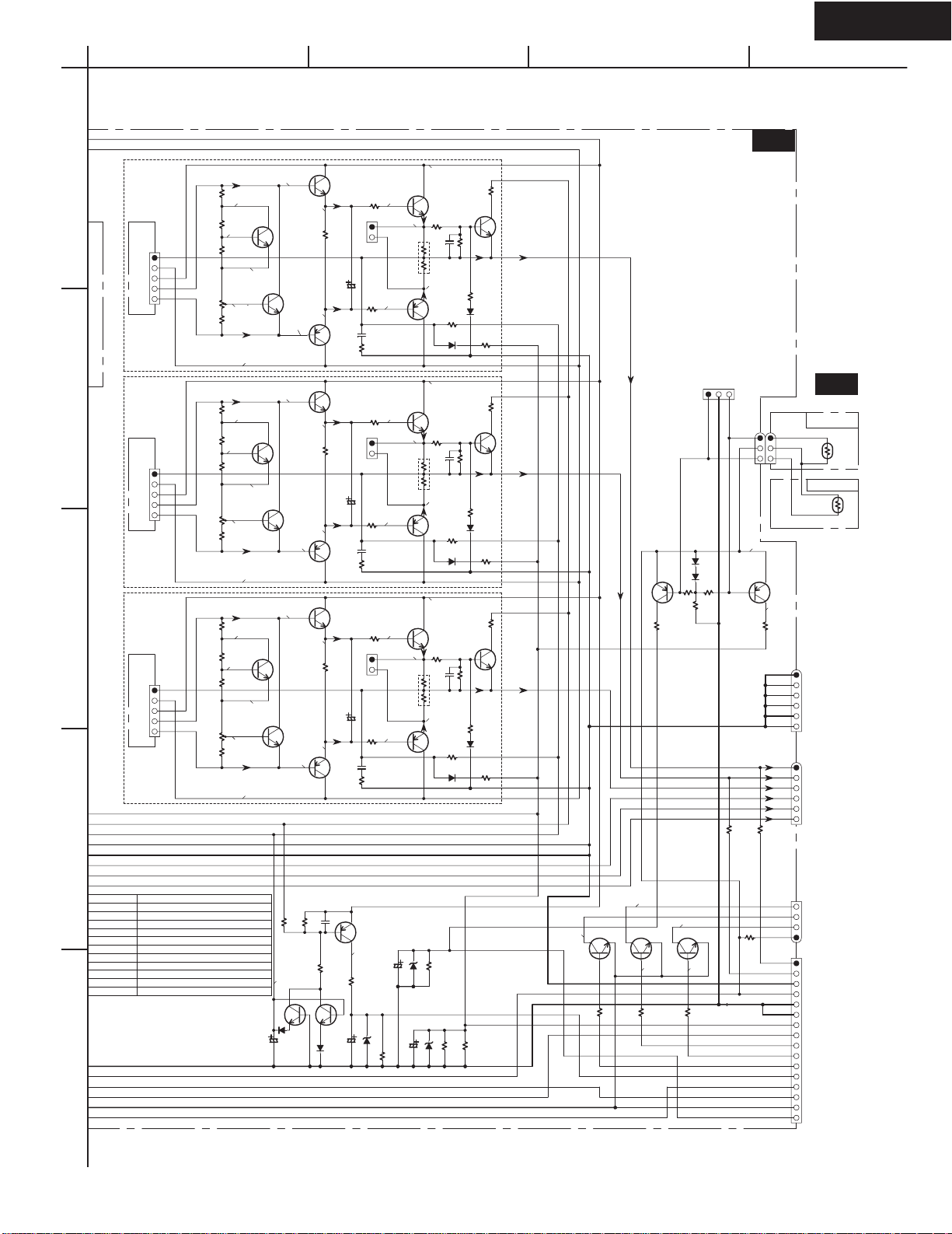
SCHEMATIC DIAGRAM 5
NAAF-7842
1
2
3
SL
R6033
470
R6003
5.6K
P6003
R6013
3.9K
NF
-B1 E
+B1 E
B+ E
(SCH-3)
B- E
P6004
NF
-B1
+B1
B+
B-
P6005
NF
-B1
+B1
B+
B-
R6043
1K
R6053
3.9K
R6034
470
R6004
5.6K
R6014
3.9K
R6044
1K
R6054
3.9K
R6035
470
R6005
5.6K
R6015
3.9K
R6045
1K
R6055
3.9K
TO NAAF-7830
SR
(SCH-3)
TO NAAF-7830
SB
(SCH-3)
TO NAAF-7830
0.2V
Q6013
R6023
-0.3V
1V
0.2V
R6024
-0.3V
0.2V
R6025
-0.3V
1V
-0.3V
-48.6V
[-58.2V]
Q6014
-0.3V
-48.6V
1V
Q6015
-0.3V
-48.6V
1.1V
1.1V
1.1V
(1/4W)
Q6023
-1.1V
Q6043
Q6024
-1.1V
Q6044
Q6025
-1.1V
Q6045
BCD
Power amplifier section
0V
R6103
(2W)
0V
R6104
(2W)
0V
R6105
(2W)
Q6053
R6143
C6053
223J
0V
Q6063
R6173
Q6054
R6144
22K
C6054
223J
0V
Q6064
R6174
Q6055
R6145
22K
C6055
223J
0V
Q6065
R6175
48.6V
R6153
12K
47K
D6003
48.6V
R6154
12K
47K
D6004
48.6V
R6155
12K
47K
D6005
22K
0.5V
R6073
100
[110]
-0.5V
0.5V
R6074
100
(1/4W)
-0.5V
0.5V
R6075
100
(1/4W)
-0.5V
Q6033
C6043
47/50
Q6034
C6044
47/50
Q6035
C6045
47/50
R6083
2.2
(1/4W)
P6083
ID+
ID-
R6093
2.2
(1/4W)
8.2
R6084
(1/4W)
P6084
ID+
ID-
R6094
2.2
(1/4W)
8.2
R6085
(1/4W)
P6085
ID+
ID-
R6095
2.2
(1/4W)
8.2 (1W)
C6233
473J
R6233
(1W)
2.2
C6234
473J
R6234
(1W)
2.2
C6235
473J
R6235
0.5V
0.22X2
-0.5V
0.5V
0.22 X2
-0.5V
0.5V
0.22 X2
-0.5V
R6163
33K
Q6073
R6193
D6013
R6183
R6164
33K
Q6074
R6194
D6014
R6184
R6165
33K
Q6075
R6195
220K
D6015
R6185
220K
47K
220K
47K
47K
U21
E
E
E
E
E
P6011
TO NAAF-7830
(SCH-3)
TO NAAF-7830
TO NAAF-7830
TO NAAF-7830
(SCH-3)
(SCH-3)
(PART-4)
4
5
P931
+13VS
+13VS
MPUGND
MPUGND
(SCH-5)
POWER
TO NAPS-7845
C6901
10000/56
10000/56
C6903
104J
P6906
C6902
C6708
223Z
D6903,6904:
D6904
D6903
R6905
0
(1/2W)
R6904
0
(1/2W)
RBV602
D5SBA20
RS603M
C6907
104J
C6905
334J
C6904
334J
C6906
104J
F6901
JL6951A
RL6902
RL6901
*
TO NAPS-7846
(SCH-5)
D6906
TYPE F6901,6902
D8A/125V
P T8AL250V
G T8AL250V
W
F6902
TO NAPS-7846
JL6952A
(SCH-5)
T8AL250V
*
C6920
0.1V
Q6901
0.8V
R6605
8.2
(1/2W)
R6902
SEMICONDUCTORS
NO.
Q6010-6015 2SC1740S-R,S
Q6020-6025 2SC1740S-R,S
Q6030-6035 KTD2061-Y OR 2SC5171
Q6040-6045 KTB1369-Y OR 2SA1930
Q6050-6055 MN100S-Y,P,O OR KTD1047-Y,O
Q6060-6065 MP100P-Y,P,O OR KTB817-Y,O
Q6070-6075 KTC3200-BL,GR OR 2SC1775A-E,F OR 2SC1845-E,F
Q6601-6603,Q6901 KTC3199-GR,2SC1740S-R,S,2SC2458-GR
1K
Q6701,6702 KTC3200-BL,GR OR 2SC1775A-E,F OR 2SC1845-E,F
Q6703 KTA1268-GR,BL OR 2SA992-E,F
Q6303
KTA1267-GR OR 2SA933S-R,S
TX-SR501/E
TO
NAAF 7830
Page 19
A
SCHEMATIC DIAGRAM 5
1
(SCH-3)
2
3
L
P6000
NF
-B1
+B1
B+
(SCH-3)
B-
TO NAAF-7830
R
P6001
NF
-B1
+B1
B+
(SCH-3)
B-
TO NAAF-7830
C
P6002
NF
-B1
+B1
B+
(PART-4)
B-
TO NAAF-7830
R6030
470
R6000
5.6K
R6010
3.9K
R6040
1K
R6050
3.9K
R6031
470
R6001
5.6K
R6011
3.9K
R6041
1K
R6051
3.9K
R6032
470
R6002
5.6K
R6012
3.9K
R6042
1K
R6052
3.9K
4
0.2V
-0.3V
0.2V
-0.3V
0.2V
-0.3V
1V
Q6010
-48.6V
1V
Q6011
-48.6V
1V
Q6012
-48.6V
1.1V
-0.3V
Q6020
-1.1V
Q6040
1.1V
(1/4W)
-0.3V
Q6021
-1.1V
Q6041
1.1V
(1/4W)
-0.3V
Q6022
-1.1V
Q6042
0.5V
R6070
100
(1/4W)
-0.5V
0.5V
R6071
100
-0.5V
0.5V
R6072
100
-0.5V
BCD
Power amplifier section
0.5V
0V
R6100
0.22 X2
(2W)
-0.5V
0.5V
0V
R6101
0.22 X2
(2W)
-0.5V
0.5V
0V
R6102
0.22 X2
(2W)
-0.5V
48.6V
Q6050
R6140
C6050
223J
R6150
12K
0V
[0V]
Q6060
R6170
47K
D6000
48.6V
Q6051
R6141
C6051
223J
R6151
12K
0V
Q6061
R6171
47K
D6001
48.6V
Q6052
R6142 22K
C6052
223J
R6152
12K
0V
Q6062
R6172
47K
D6002
22K
22K
R6160
33K
Q6070
R6190
D6010
R6180
R6161
33K
Q6071
R6191
D6011
R6181
R6162
33K
Q6072
R6192
220K
D6012
R6182
220K
47K
220K
47K
47K
Q6030
C6040
47/50
Q6031
C6041
47/50
Q6032
C6042
47/50
R6080
(1/4W)
P6080
ID+
ID-
R6090
2.2
(1/4W)
8.2
R6081
2.2
(1/4W)
P6081
ID+
ID-
R6091
2.2
(1/4W)
8.2
R6082
(1/4W)
P6082
ID+
ID-
R6092
2.2
(1/4W)
8.2 (1W)
2.2
C6230
473J
R6230
(1W)
C6231
473J
R6231
(1W)
2.2
C6232
473J
R6232
TH2
P6301
TH2
D6307
*
Q6313
D6306
R6317
*
2.2K
* P/DG-TYPE ONLY
*
R6306
R6318
10K
4.7K
R6851
390
(1/2W)
TH1
COM
+24V
R6307
2.2K
TH1
LSP
RSP
CSP
LSSP
RSSP
SBSP
U21
JL6402A
24V
Q6303
LSPE
RSPE
CSPE
SBSPE
R6850
(1/2W)
U28
[PTH9M04BF
JL6402B
P/W/G-TYPE ONLY
0V
R6308
4.7K
LSSPE
RSSPE
390
222TS2F333]
NAETC-7849
THERMISTOR
NAETC-7850
R6381
[PTH9M04BC
222TS2F333]
JL6804A
(SCH-5)
TO NAETC-7835
JL6803A
(SCH-5)
TO NAETC-7835
R6380
SEMICONDUCTORS
NO.
Q6010-6015 2SC1740S-R,S
Q6020-6025 2SC1740S-R,S
Q6030-6035 KTD2061-Y OR 2SC5171
Q6040-6045 KTB1369-Y OR 2SA1930
Q6050-6055 MN100S-Y,P,O OR KTD1047-Y,O
Q6060-6065 MP100P-Y,P,O OR KTB817-Y,O
Q6070-6075 KTC3200-BL,GR OR 2SC1775A-E,F OR 2SC1845-E,F
Q6601-6603,Q6901
Q6701,6702 KTC3200-BL,GR OR 2SC1775A-E,F OR 2SC1845-E,F
Q6703 KTA1268-GR,BL OR 2SA992-E,F
Q6303
KTC3199-GR,2SC1740S-R,S,2SC2458-GR
KTA1267-GR OR 2SA933S-R,S
5
R6702
10K
R6701
22K
0V
Q6701 Q6702
D6701
C6701
100/6.3
C6703
223Z
R6708
C6704
1/50
D6702
33K
+B1
Q6703
0V
C6716
100/6.3
R6704
47K
D6703
MTZJ5.1B
R6706
220K
*
D6714
MTZJ5.1B
*
R6719
*
* P/W/G-TYPE ONLY
D6704
MTZJ5.1B
C6706
100/6.3
5.6K
R6709
5.6K
R6710
47K
24V
24V
0.05V
R6601
1K
+13VS POWER
POWER
Q6602Q6603Q6601
0V 0V
R6603
R6602
1K
1K
MPUGND
MPUGND
BRLD
FRLD
CSRLD
+24V
(1/2W)
HPL
R6604
8.2
HPR
E
+24V
VOLH
SEC1H
SPB
SPCS
SPF
PRO
+13VS
RLGND
PROTHERM
JL6805A
(SCH-5)
TO NAETC-7835
P6931NAETC-7833
(SCH-5)
 Loading...