

ONKYO ® SERVICE MANUAL
QUARTZ SYNTHESIZED FM STEREO/AM TUNER MODEL T08
QUARTZ SYNTHESIZED FM STEREO/MW/LW TUNER MODEL T08L
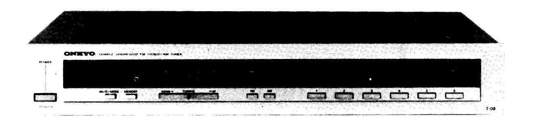
TABLE OF CONTENTS
| ltem | Page |
|---|---|
| Specifications | 2 |
| Precautions | 3 |
| Exploded view (T-08) | 4 |
| Parts list (T-08) | 5 |
| Disassembling procedures | 5 |
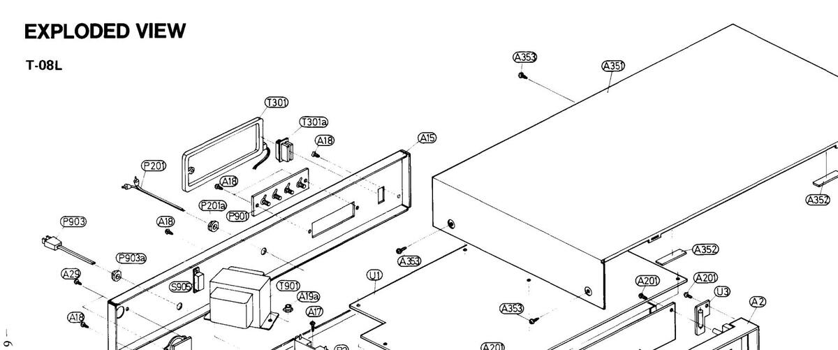
| Exploded view (T-08L) | 6 |
| Parts list | 7 |
| Block diagram of IC | 7 |
| Circuit description | 10 |
| Block diagram (T-08) | 15 |
| Adjustment procedures | 16 |
| Pc board view from component side (W model) | 19 |
| Pc board-parts list (D/W models) | 21 |
| Pc board view from component side (D model) | 23 |
| Schematic diagram (D/W models) | 25 |
| Pc board view from component side (G model) | 27 |
| Schematic diagram (G model) | 29 |
| Pc board-parts list (G model) | 31 |
| Pc board-parts list (T-08L) | 33 |
| Pc board view from component side (T-08L) | 35 |
| Schematic diagram (T-08L) | 37 |
| Block diagram (T-08L) | 39 |
| Packing view | 40 |

SPECIFICATIONS
T-08D
FΜ
Tuning Range: Usable Sensitivity:
50 dB Quieting Sensitivity:
Capture Ratio: Image Rejection Ratio: IF Rejection Ratio: Signal-to-Noise Ratio:
Alternate Channel Att. : AM Suppression Ratio:
Frequency Response: Stereo Separation:
Output Voltage: Muting Level:
AM:
Tuning Range: Usable Sensitivity: Image Rejection Ratio: IF Rejection Ratio: Signal-to-Noise Ratio: Total Harmonic Distortion: Output Voltage:
General
Power Supply: Antennas:
ntennas:
Semiconductors:
Dimensions (W x H x D):
Weight:
Stereo: 17.2 dBf, 4.0 µV Mono: 16.1 dBf, 3.5 µV Stereo: 36.1 dBf, 35 µV 1.5 dB 45 dB 85 dB Mono: 73 dB Stereo: 65 dB 60 dB IHE (+400 kHz) 50 dB Mono: 0.15% Stereo: 0.25% 30 - 15.000 Hz ± 1.5 dB 40 dB at 1 kHz 30 dB at 100 - 10.000 Hz 500 mV 300 mV 530 - 1620 kHz (10 kHz steps) 25 µV 45 d B 30 d E 40 d B 150 mV AC 120 volts 60 Hz FM: 300 ohms balanced and
87.9 - 107.9 MHz (200 kHz steps)
Mono: 10.8 dBf, 1.9 µV, IHF
AC 120 volts, 60 Hz FM: 300 ohms balanced and 75 ohms unbalanced AM: built-in loop antenna and external terminal 4 FETs, 36 transistors, 12 ICs, 48 diodes, 15 LEDs 418 x 72 x 275 mm (16-1/2" x 2-7/8" x 10-13/16") 3.4 kg, 7.5 lbs.
* Specifications and features are subject to change without notice
T-08G/W/Q
FM:
Tuning Range: 87.5 - 108.0 MHz (50 kHz steps) 87.9 - 107.9 MHz (200 kHz step: for Canadian Model) Usable Sensitivity: Mono: 10.8 dBf. 1.9 µV. IHF 1.6 µV (S/N 26 dR 40 kHz Dev.) DIN Stereo: 17.2 dBf, 4.0 µV, IHF 50 µV (S/N 46 dR 40 kHz Dev ) DIN 50 dB Oujenting Sensitivity: Mono: 161 dBf 35 uV Stereo: 36.1 dBf 35 uV Capture Ratio: age Rejection Ratio IF Rejection Ratio 85 dB Signal-to-Noise Ratio: Mono: 73 dB Stereo: 65 dB Selectivity: 55 dB DIN (± 300 kHz, 40 kHz Dev.) AM Suppression Ratio: 50 d B Total Harmonic Distortion: Mono: 015% Stereo: 0.3% Frequency Response: 30 – 15.000 Hz ± 1.5 dB Stereo Separation: 40 dB at 1 kHz 30 dB at 100 - 10,000 Hz Output Voltage: Muting Level: 13.2 dBf, 2.5 μF MW. Tuning Range: 522 – 1611 kHz (9 kHz steps) 530 – 1620 kHz (10 kHz step: for Canadian Model) Usable Sensitivity: 25 µV Image Rejection Ratio: IF Rejection Ratio: 30 dB Signal-to-Noise Ratio: 40 dB Total Harmonic Distortion: 0.8% Output Votage: General Power Supply: European Models: AC 220 V. 50 Hz British & Australian Models: AC 240 V, 50 Hz Worldwise Models: AC 120 V 60 Hz/ AC 220 V, 50 Hz Antennas FM: 300 ohms balanced and 75 ohms unbalanced AM : built-in loop antenna Semiconductors: 4 FETs, 36 transistors, 12 ICs, 48 diodes, 13 LEDs Dimensions (W x H x D): 418 × 72 × 275 mm (16-1/2" x 2-7/8" x 10-13/16") Weight: 3.4 kg, 7.5 lbs.
* Specifications and features are subject to change without notice.
T-08L
| FM· | 1 | |
|---|---|---|
| Tuning Range: | 87.5 - 108.0 MHz (50 kHz steps) | ( |
| Usable Sensitivity: |
Mono: 10.8 dBf, 1.9 μV, 1HF
1.6 μV (S/N 26 dB, 40 kHz Dev.) DIN |
|
- 1 |
|
Stereo: 17.2 dBf, 4.0 µV, IHF
50 µV (S/N 46 dB, 40 kHz Dev.) DIN |
I
I S |
|
| 50 dB Quieting Sensitivity: |
Mono: 16.1 dBf, 3.5 μV
Stereo: 36.1 dBf, 35 μV |
|
| Capture Ratio: | 1.5 dB | |
| Image Rejection Ratio: | 45 dB | |
| IF Rejection Ratio: | 85 dB | |
| Signal-to-Noise Ratio: | Mono: 73 dB | |
| Stereo: 65 dB | ||
| Selectivity: | 55 dB DIN (± 300 kHz, 40 kHz Dev.) | |
| AM Suppression Ratio: | 50 dB | |
| Total Harmonic Distortion: | Mono: 0.15% | |
| Stereo: 0.3% | ||
| Frequency Response: | 30 - 15,000 Hz ± 1.5 dB | |
| Stereo Separation: | 40 dB at 1 kHz | |
| 30 dB at 100 – 10,000 Hz | 5 | |
| Output Voltage: | 500 mV | |
| Muting Level: | 13.2 dBf, 2.5 μV | I |
| MW: | ||
| Tuning Range: | 522 – 1611 kHz (9 kHz steps) | | \ |
| Usable Sensitivity: | 25 μV | |
| Image Rejection Ratio: | 45 dB |
| IF Rejection Ratio: | 30 a B |
|---|---|
| Signal-to-Noise Ratio: | 40 dB |
| Total Harmonic Distortion: | 0.8% |
| Output Voltage: | 150 mV |
| LW: | |
| Tuning Range: | 146 – 353 kHz (9 kHz steps) |
| Usable Sensitivity: | 35 µV |
| Image Rejection Ratio: | 30 dB |
| IF Rejection Ratio: | 30 d B |
| Signal-to-Noise Ratio: | 40 d B |
| Total Harmonic Distortion: | 0.8% |
| Output Voltage: | 150 mV |
| General | |
| Power Supply: | European Models: AC 220 V, 50 Hz |
| Canadian Models: AC 120 V, 60 Hz | |
| British & Australian Models: | |
| AC 240 V, 50 Hz | |
| Worldwise Models: AC 120 V, 60 Hz/ | |
| AC 220 V, 50 Hz | |
| Antennas: | FM: 300 ohms balanced and |
| 75 ohms unbalanced | |
| AM (MW/LW): built-in loop antenna | |
| and external terminal | |
| Semiconductors: | 4 FETs, 36 transistors, 12 ICs |
| 48 diodes, 15 LEDs | |
| Dimensions (W x H x D): | 418 × 72 × 275 mm |
| (16-1/2" × 2-7/8" × 10-13/16") | |
| Weight: | 3.4 kg, 7.5 lbs. |
* Specifications and features are subject to change without notice.
PRECAUTIONS
1. Replacing the C MOS IC
- 1. All MOS devices should be stored or transported in materials that are somewhat conductive. MOS devices must not be inserted into conventional plastic "snow" or plastic trays.
- 2. All MOS devices should be placed on a grounded bench surface and operators should ground themselves prior to handling devices, since a worker can be statically charged with respect to the bench surface.
- 3. Nylon clothing should not be worn while handling MOS circuits.
- 4. When lead straightening or hand soldering is necessary, provide ground straps for the apparatus used.
- 5. Double check test equipment setup for proper polarity of voltage before conducting parametric or functional testing.
- 6. All unused device inputs shoud be connected to VDD or VSS.
2. Memory Preservation Batteries
Because stations stored in the memory by the FM/AM preset keys would normally be lost when power is turned off or the plug removed from the wall socket, this unit requires two memory preservation batteries to preserve the contents of the memory even when power is turned off. Be sure to insert the correct type of batteries into the battery holder in the bottom of the unit before turning on power for the first time.
3. Voltage Selector (rear panel)
120/220V models are equipped with a voltage selector to conform with local power supplies. Be sure to set this switch to match the voltage of the power supply in your area before turning the power switch on. Voltage is changed by sliding the groove in the switch with a screwdriver or similar instrument to the top or bottom position. Confirm that the switch has been moved all the way up or down before turning the power switch on. If there is no voltage selector switch on the unit you have purchased, it can only be used in areas where the power supply voltage is the same as that of the unit.
4. De-Emphasis Switch (rear panel)
120/220V models are equipped with a 50µsec - 75µsec selector switch. This switch is set to 50µsec at the factory, but may have to be reset 75µsec depending on the area where the unit is used:
- Europe: 50µsec
- U.S.A. : 75 µsec
5. AM Tuning Step Frequency Switch (bottom panel)
120/220V models are equipped with a switch to change the AM Tuning step frequency from 9kHz. These units are set to 9kHz at the factory; change to 10kHz if this gives better results in your locality.
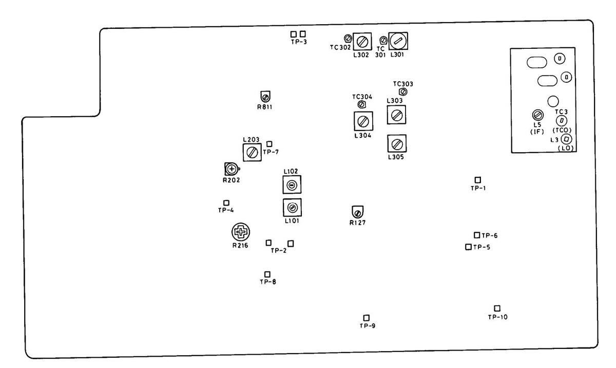
EXPLODED VIEW
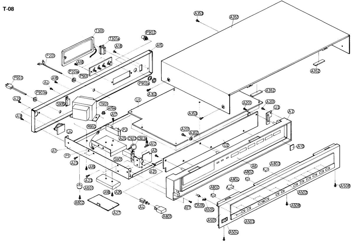
PARTS LIST
| REF, NO. | PARTS NO. | DESCRIPTION | REF. NO. | PARTS NO. | DESCRIPTION |
|---|---|---|---|---|---|
| A1 | 27100048 | Chassis | C922 | 3500065A | 0.01 µF, 400V, Capacitor IS |
| A2 | 27110127-1B | Front bracket | C922a | 27300080 | Cover, capacitor |
| A3 | 27140526 | Bracket, switch | D505 | 225070 | SLP-144B, L.E.D, muting indicator |
| A4 | 27260062 | Shaft, switch | P1 | 223004 | Terminal |
| A6 | 13218901 | Back plate ass'y | P2 | 25108010 | LG-2C, Terminal |
| A7 | 27267159A | Guide, L.E.D | P201 | 2010039 | PN-B, Output cable |
| A8 | 28191072 | Clear plate S | P201a | 270025 | SR-3P-4, Strainrelief |
| A9 | 28130103A | Dial plate | P 901 | 25060035 | NTM-4PRMC06, Terminal, antenna |
| A10 | 28140333 | Cushion | P902 | 25045088 | 75Ω antenna connector (G) |
| A12 | 27190038 | Holder | P902a | 870057 | M10B, Toothed washer (G) |
| A15 | 27120407 | Back panel (D) | P903 | 253099A | AS-UC-3, Power supply cable (D) |
| 27120408 | Back panel (G) | P903a | 270025 | SR-3P-4, Strainrelief (D) | |
| 27120409 | Back panel (W) | P903 | 253083 | AS-CEE, Power supply cable (G/W) | |
| A17 | 834130088 | 3TTS+8B, Tapping screw | P903a | 270280 | SR-4K-4, Strainrelief (G/W) |
| A18 | 834130068 | 3TTS+6B, Tapping screw | R950 | 431523355 | 3.3MΩ, 1/2W, Registor, solid (D) |
| A19 | 834140108 | 4TTS+10B, Tapping screw (D/W) | S901 | 25035135 | NPS-111-L100P, Power switch (D) |
| 82114010 | 4P+10FN, Pan head screw (G) | S901 | 25035322 or | NPS-111-L286P or | |
| A19a | 86214010 | WN4x6FN, Washer head nut (G) | 25035176 | NPS-111-L140, Power switch (G/W) | |
| A21 | 82113006 | 3P+6FN, Pan head screw | S905 | 25065123 | NSS-1258P, Voltage selector (W) |
| A23 | 838130068 | 3TTB+6B, Tapping screw | T301 | 232085 | NMA-3034, AM loop antenna |
| A25 | 27140461-1 | Battery bracket | T301a | 27190105 | Holder, AM loop antenna |
| A26 | 27300360 | Battery case | T901 | 230467A | NPT-734D, Power transformer (D) |
| A27 | 27300359 | Lid | 230468 | NPT-734G, Power transformer (G) | |
| A29 | 82112604 | 2.6P+4F, Pan head screw | 230469 | NPT-734DG, Power transformer (W) | |
| A201 | 831130080 | 3TTW+8P, Tapping screw | U1 | 13218527 | NARF-1427, FM/AM tuner pc |
| A202 | 870069 | W10x5, Nylon washer | board ass'y (D) | ||
| A351 | 28184104 | Top cover | 13224527A | NARF-1427a, FM/AM tuner pc | |
| A352 | 28140020 | 4x10x40mm, Cushion | board ass'y (G) | ||
| A353 | 834430068 | 3TTS+6B (BC), Tapping screw | 13220527B | NARF-1427b, FM/AM tuner pc | |
| A501 | 13218121 | Front panel ass'y | board ass'y (W) | ||
| A502 | 28191073C | Clear plate | U2 | 13218528 | NADIS-1428, Display pc board ass'y (D) |
| A503 | 27267176B | Plate | 13224528A | NADIS-1428a, Display pc board | |
| A504 | 27267109 | Guide, power | ass'y (G/W) | ||
| A505 | 27190160 | Holder, L.E.D | U3 | 13218529 | NAPL-1429, Dial illumination lamp |
| A508 | 831130080 | 3TTW+8P, Tapping screw | pc board ass'y | ||
| A601 | 27175018 | Leg | U4 | 13218530 | NARM-1430, Remote terminal pc |
| A602 | 834130108 | 3TTS+10B, Tapping screw | board ass'y | ||
| A801 | 28320573 | Knob, power | |||
| A802 | 28320501 | Knob, MW/Memory/FM/AM/ | Note: D: 0 | Only 120V model | |
| Muting | G: ( | Only 220V model | |||
| A803 | 28320502 | Knob, station | W: 0 | Only 120/220V mc | odel |
| A804 | 28320503 | Knob, UP/DOWN |
DISASSEMBLING PROCEDURES
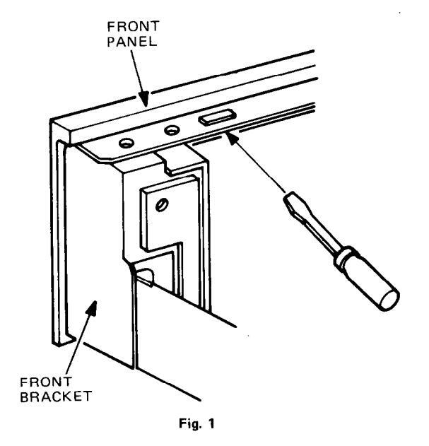
1. Removal of front panel
- 1. Remove the four screws (A353) holding the side bracket and the top cover.
- Remove a screw (A353) holding the top cover and back panel.
- 3. Remove the three screws (A508) holding the front panel and front bracket from bottom side.
- Insert the driver between the front panel and front bracket as shown in the fig. 1, and remove the front panel from the projection of the front bracket.
2. Removal of the digital pc board
- 1. Remove the top cover and the front panel.
- Remove the three screws (A17) holding the front bracket and digital pc board from the front side.
- 3. Remove the seven screws (A201) holding the digital pc board and the front bracket.
AD
A23
Å23
A18 A2
A27
() (A60)
(A60
--------------------------------------
A502
A508
A 508
, (4803) S
A503
(480) (1) (1
C
(A50)
•
A504)
(1) (AI)
(D505
PARTS LIST
| REF. NO. | PARTS NO. | DESCRIPTION | REF. NO. | PARTS NO. | DESCRIPTION |
|---|---|---|---|---|---|
| A1 | 27100048 | Chassis | A602 | 834130108 | 3TTS+10B, Tapping screw |
| A2 | 27110127-1B | Front bracket | A801 | 28320573 | Knob, power |
| A3 | 27140526 | Bracket, switch | A802 | 28320501 | Knob, MW/Memory/FM/MW/LW/ |
| A4 | 27260062 | Shaft, switch | Muting | ||
| A6 | 13520901 | Back plate ass'y | A803 | 28320502 | Knob, station |
| A7 | 27267198 | Guide, L.E.D | A804 | 28320503 | Knob, UP/DOWN |
| A8 | 28191072 | Clear plate S | C922 | 3500065A | 0.01 µF, 400V, Capacitor IS |
| A9 | 28130103A | Dial plate | C922a | 27300080 | Cover, capacitor |
| A10 | 28140333 | Cushion | D505 | 225070 | SLP-144B, L.E.D, muting indicator |
| A12 | 27190038 | Holder | P1 | 223004 | Terminal |
| A15 | 27120410 | Back panel | P2 | 25108010 | LG-2C, Terminal |
| A17 | 834130088 | 3TTS+8B, Tapping screw | P201 | 2010039 | PN-B, Output cable |
| A18 | 834130068 | 3TTS+6B, Tapping screw | P201a | 270025 | SR-3P-4, Strainrelief |
| A19 | 82114010 | 4P+10FN, Pan head screw | P9 01 | 25060035 | NTM-4PRMC06, Terminal, antenna |
| A19a | 86214010 | WN4×10FN, Washer head nut | P9 03 | 253083 | AS-CEE, Power supply cable |
| A21 | 82113006 | 3P+6FN, Pan head screw | P903a | 270280 | SR-4K-4, Strainrelief |
| A23 | 838130068 | 3TTB+6B, Tapping screw | S901 | 25035322 or | NPS-111-L286 or |
| A25 | 27140461-1 | Battery bracket | 25035176 | NPS-111-L140, Power switch | |
| A26 | 27300360 | Battery case | T301 | 232085 | NMA-3034, AM loop antenna |
| A27 | 27300359 | Lid | T301a | 27190105 | Holder, AM loop antenna |
| A29 | 82112604 | 2.6P+4F, Pan head screw | T901 | 230468 | NPT-734G, Power transformer |
| A201 | 831130080 | 8TTW+8P, Tapping screw | U1 | 13520527C | NARF-1427C, FM/AM tuner pc |
| A202 | 870069 | W10x5, Nylon washer | board ass'y | ||
| A351 | 28184104 | Top cover | U2 | 13520528B | NADIS-1428b, Display pc board |
| A352 | 28140020 | 4x10x40mm, Cushion | ass'y | ||
| A353 | 834430068 | 3TTS+6B (BC), Tapping screw | U3 | 13218529 | NAPL-1429, Dial illumination |
| A501 | 13520121 | Front panel ass'y | lamp pc board ass'y | ||
| A503 | 27267177B | Plate | U4 | 13218530 | NARM-1430, Remote terminal pc |
| A504 | 27267109 | Guide, power | board ass'y | ||
| A505 | 27190160 | Holder, L.E.D | U5 | 13520531 | NALED-1431, Memory indicator |
| A508 | 831130080 | 3TTW+8P, Tapping screw | pc board ass'y | ||
| A601 | 27175018 | Leg | |||
BLOCK DIAGRAM OF IC
μPC1167C2 (FM IF system)

HA1196 (MPX decoder)

4066B (Quad bilateral switch)
HA1197 (AM radio system)
• 74LS42 (BCD to DECIMAL Decoder)
Pin Connection Diagram

Function Table

Pin Connection
Pin 1 (Vcc) ..... +5 volts Supply Pin 2 (IN) ..... FM local oscillator signal input Pin 3 (CHK) ..... Check terminal Pin 4 (GND) ..... Ground terminal Pin 5 (OUT) ..... Prescaler terminal Pin 6 (PSC) ..... Prescaler control terminal Pin 7.8 ..... Not connected
Timing Chart
Logic Diagram
- 8 -
Pin Connection Diagram
| 10- | INPL | tn (OUTPUTS) | |||
|---|---|---|---|---|---|
| CL | J | R | R | Qn-I | Qn |
| 0 | x | 0 | 0 | 0 | |
| , | x | 0 | 0 | 1 | |
| 5 | × | 0 | ο | 1 | 0 |
| 5 | ' | 0 | 0 | Qn-1 | Qn-I MODE |
| 5 | × | 1 | 0 | 1 | 1 |
| x | x | 0 | Qn-I | Qn-i | |
| × | × | × | , | × | 0 |
First Stage Truth Table
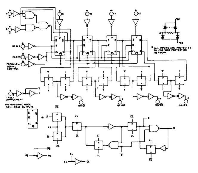
Logic Diagram
CIRCUIT DESCRIPTION
1. Micro Computer Operation
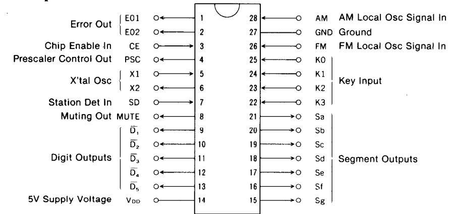
|
Pin.
No. |
Symbol | Terminal | Description | |
|---|---|---|---|---|
| 1 2 |
E01
E02 |
Error
Outputs |
Charge pump output of the phase detector which constitutes the PLL.
HIGH level is output when the divided oscillation frequency is higher than the reference frequency. In the opposite case, LOW level is output. Floating occurs when the frequen- cies match. The output is applied to the variable capacitor in the front end through low pass filters Q403 and Q404. The output from both terminals is Only E01 is used. |
|
| 3 | CE |
Chip Enable
Input |
Device selection signal input terminal. HIGH levelnormal operation;
LOW levelmemory preservation. |
|
| 4 | PSC |
Preset
Control Output |
This terminal outputs a signal that switches the prescaler division ratio to 1/16 or 1/17 when the pulse swallow method is used for division (FM only). | |
|
5
6 |
X1
X2 |
X'tal | Connected to the 4.5MHz crystal oscillator. | |
| 7 | SD |
Station
Detector Input |
Input terminal for detecting whether or not a broadcast signal is being received during auto-tuning.
Stopped by the HIGH level. Not used. |
|
| 8 | MUTE |
Muting
Output |
Output terminal which mutes the shock noise occurring when the PLL is released; active HIGH. | |
| 9—13 | D1—D5 |
Digit
Outputs |
Display digit output signal terminals; active LOW. | |
| 14 | VDD |
Supply
Voltage |
Device power terminal; supplies 5V during normal operation and 3V from the external power source (two batterries) for memory preservation. | |
| 15—21 | Sa—Sg |
Segment
Outputs |
Display tube segment signal output, key return signal source and station
display signal terminals; active HIGH. Since these terminals can handle 30V, they are connected directly to the segment terminals of the fluorescent display tubes. |
|
| 22—25 | K0—K3 |
Key Return
Signal Inputs |
Terminals for input of the key return signals from the external key matrix. | |
| 26 | FM |
FM Local
Oscillator Signal Inputs |
FM signals received are divided by 1/16 or 1/17 by prescaler µPB553AC for input to this terminal. | |
| 27 | GND | Ground | ||
| 28 | АМ |
AM Local
Oscillator Signal Input |
Terminal for input of AM broadcast signal. | |
2. Control Key Connections
UP, DOWN.....Pressing the UP or DOWN key will cause the frequency to be shifted upward or downward (in 200kHz steps with the D model and in 50 kHz steps with the W/G model). If the key is pressed for more than 0.5 seconds, the frequency will be shifted 50 kHz every 40ms until it is released.
MW, FM, LW.....The MW, FM, LW band switches.
MEMORY.....Pressing this key causes the memory to be placed in the write-enabled state. The frequency displayed will be stored in one of the memories 1—6 if the corresponding memory key is then pressed within 5 seconds. The write-enabled state will be cleared after 5 seconds if none of the memory keys are pressed, or if the AM/FM selector keys are pressed.
M1—M7(M6).....These keys are used to preset and recall the contents of the memory. Positions are provided for keys for reading / writing up to 7 frequencies, but only 6 keys are installed in the T-08. See the paragraph on MEMORY for writing frequencies. Pressing one of the
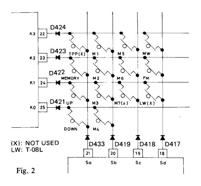
keys M1—M6 once will cause the contents of the corresponding memory (a frequency) to be read. A muting signal of about 0.45 seconds duration is output at this time.
TPP (Tracking Point Preset).....Switch is used to write adjustment frequencies into preset memory during set production. Not used with the T-08. When the IC Vpp is first inserted, the lowest FM and MW frequency is placed in the memory.
| K3 22 |
Inpui
Termina Output Terminal |
K0 (25) | K1 (24) | K2 (23) | K3 (22) |
|---|---|---|---|---|---|
| К1 24 | Sf (16) | 9kHz/10kHz | AUTO/MANU | ||
| Sg (15) | BAND 0 | BAND 1 | IF 1 | IF 0 | |
| D416 D415 | Not used | table | |||
| 220V (G model) | hen the diode is connected | ||||
| Fig. 2 Sf Sg D415 and | 416 are not used for 120V mode | el. | IF 1 | IF 0 IF F | Frequency |
3. Key Matrix Connections
IF1, IF0.....IF offset value settings for FM. See Table 2. BAND1, BAND0......Geographical FM band settings. See Table 3.
9kHz, 10kHz.....MW band settings. See Table 4.
AUTO/MANUAL.....Auto tuning for 1, manual tuning for 0. Manual only with the T-08.
| IF 1 | IF 0 | IF Frequency |
|---|---|---|
| 0 | 0 | 10.700MHz |
| 0 | 1 | 10.675MHz |
| 1 | 0 | 10.750MHz |
| 1 | 1 | 10.725MHz |
table 2
| BAND 1 | BAND 0 | Band | Frequency Range | Channel Space |
|---|---|---|---|---|
| 0 | 0 | 120V model | 87.9∿107.9MHz | 200kHz |
| 0 | 1 | 220V model | 87.50∿108.00MHz | 50kHz |
| 1 | 0 | Japan | 76.1∿89.9MHz | 100kHz |
table 3
| 9kHz/10kHz | Frequency range |
Channel
Space |
Reference
Frequency |
|---|---|---|---|
| 0 | 530~1620kHz | 10kHz | 10kHz |
| 1 | 522~1611kHz | 9kHz | 9kHz |
table 4
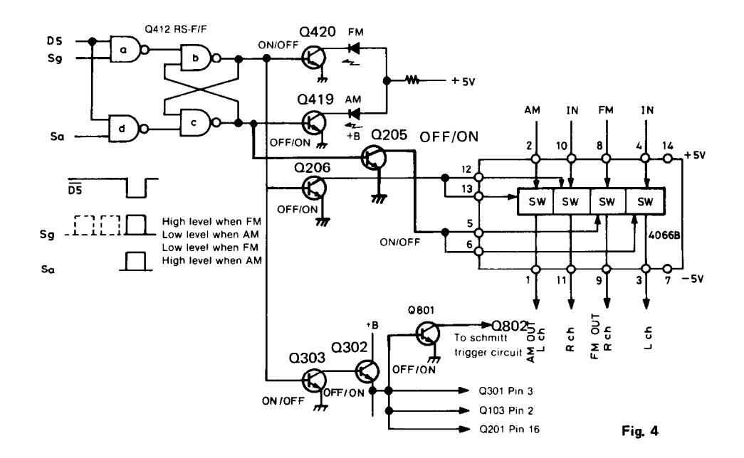
4. FM/AM Selector Circuit
The FM/AM selector circuit is shown in Figure 4. Operation of this circuit is controlled by digit signal D5 and segment output signals Sa and Sg.
For FM reception, both D5 and Sg are "H" (Sa is "L") and output from b of RS-F/F is "H." Since output from c is "L," Q420 is turned ON to light the FM indicator and Q419 is turned OFF. Further, AM operation ceases because Q303 goes ON and Q302 OFF so that B + is not supplied to AM IC Q301. Also, Q206 goes ON, turning Q205 OFF so that the FM signal is output.
For AM reception, both D5 and Sa are "H" (Sg is "L"), output from b of RS-F/F is "L"and that from c is "H" so that all transistors operate in the opposite manner, the AM indicator is lit and the AM signal is output. Further, Q304 goes ON so that B + is supplied to pin 3 of AM IC Q301 to start AM operation. Also, the level at pin 2 of IC Q103 of the FM IF system becomes "H" so that this IC does not operate and output from the 16-pin VCO also ceases.
5. Preset Station Indicator Circuit
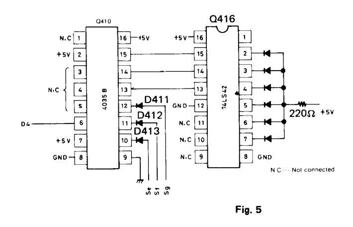
(BCD code outputs from Se—Sg)
Fig. 6
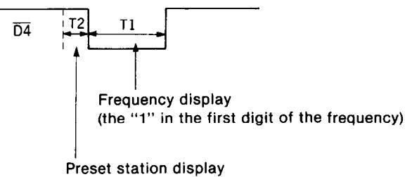
Preset station indicator connections are shown in Figure 5. BCD codes are output from segment terminals Se—Sg in synchronization with the timing of digit signal D4. The sequence is shown in the timing chart in Figure 6. The display signal for the "1" in the first digit of the frequency display is output from segment terminals. Sb and Sc at timing T1 of digit signal D4 (blank codes are output from segment terminals Se—Sg at this time). At timing T2, the BCD code
for preset station display is output from segment terminals Se—Sg (at this time, blank codes are output from segment terminals Sa—Sd). Since output is timed as shown in Figure 8, it is replaced with starting output at D—F/F of Q416. This is output as BCD code to the decimal counter to display the frequency.
6. PLL Tuned Circuit
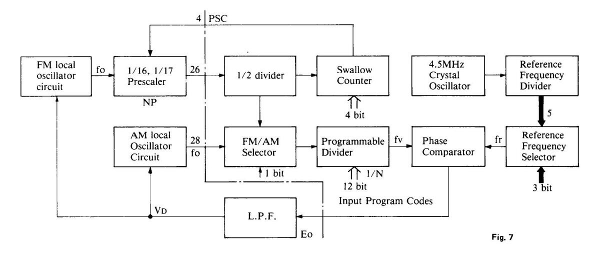
A block diagram of the tuned circuit of the PLL is shown in Figure 13.
Operation During AM Reception
The reception frequency is applied to the programmable divider where it is divided to 1/N and output as fv. This is applied to the phase detector where it is compared with frequency standard fr (9kHz for G/W model and 10 kHz for D model). If fr and fv differ, Eo equal to the difference in frequency is output. Since error output Eo is a pulse waveform, it is passed through the low pass filter to change it into DC voltage VD, which is applied to the variable capacitor in the front end to change the reception frequency. This continues until fv and fr are the same and Eo = 0. (G/W model)
Since AM signals received range from 522 kHz to 1611kHz, they are changed to 972kHz-2061kHz for reception. Furthermore, since fv = fo/N, the divisor, N, is changed by program code input so that N = 972/9-2061/9 = 108-229. (D model)
Since AM signals received range from 530kHz to 1620kHz, they are changed to 980kHz-2070kHz for reception.
Furthermore, since fv = fo/N, the divisor, N, is changed by program code input so that N = 980/10-2070/10 = 98-207. Operation During FM Reception.
The pulse swallow method is used in the prescaler of the T-25. In this type of prescaler, a supplementary number (changed according to the program code input) and the divided reception frequency from the prescaler are combined in the control counter and the prescaler's division factor is switched between 1/16 and 1/17 according to external control (1/17 when the PSC terminal is "H" and 1/16 when it is "L").
The station oscillation frequency is applied to the programmable divider, but the programmable divider has an upper frequency limit of only 30MHz, so the pulse swallow-type prescaler, which can be used up to 150MHz, is inserted for division to 1/Np.
The signal is then divided to 1/2 in the microcomputer and applied to the programmable divider and divided to 1/N. The result is compared with a 25 kHz frequency standard in the phase detector and the error is output as Eo until a match is obtained as in AM operation.
7. Muting Circuit
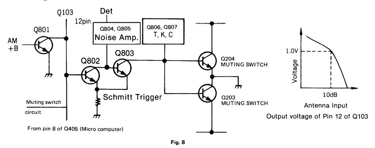
A muting circuit consisting of a zero cross and IF level detecters is built into IC O103: output of this circuit is from pin 12. R127 is the variable resistor used to set the muting level, and is set so that muting opens at 10dB. When the antenna input level exceeds 10dB, transistor Q802 is turned OFF, Q803 is turned ON, and Q203 and Q204 are turned OFF so that the FM signal is output from the output terminal. Further, this circuit closes muting when a noise element is detected in the output of noise amplifier Q804, Q805. Q801 is ON during AM reception so that all transistors operate in the above manner and the AM signal is output.
When the STATION, BAND (AM/FM), UP or DOWN switches are operated, the pulses shown in Figure 9 are output from pin 8 of O703 and muting is activated Note : The noise amplifier is not used for 120V medel.
Muting switch circuit

Band (89.9 - 76.1MHz, 76.1 - 89.9MHz)


A muting switch circuit is used the flip-flop circuit of multivibrator.
When press the MUT/MODE switch, transistor Q503 is turned OFF, Q504 is turned ON, and FM signal is output so that the Q203 and Q204 transistors operate in the above manner.
O502 is turned ON and MUT L.E.D light off. O501 is OFF during AM reception and MUT L.E.D light off.
BLOCK DIAGRAM

ADJUSTMENT PROCEDURES
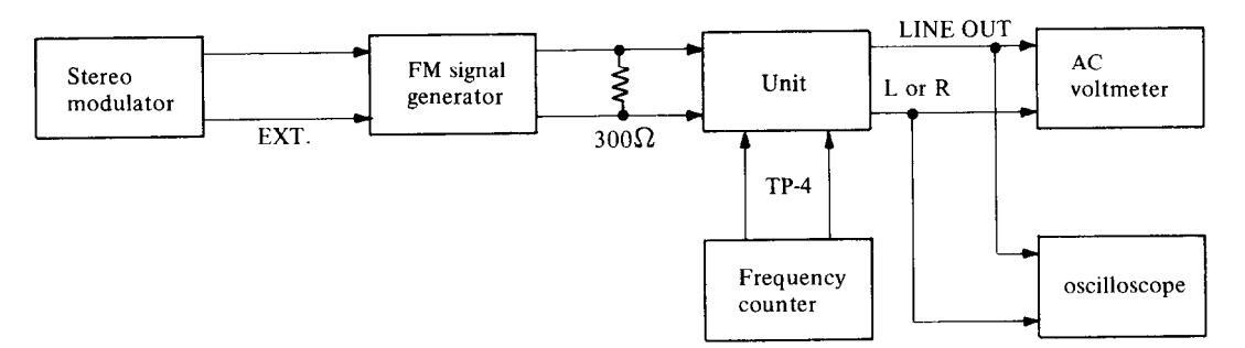
INSTRUMENTS REQUIRED
- 1. Stereo Modulator
- 2. FM Signal Generator with Frequency Counter
- Frequency Counter Digital DC Voltmeter
- 5. DC Voltmeter
- 6. Distortion Analyzer
- 7. AC Voltmeter
- 8. Oscilloscope
GENERAL ALIGNMENT CONDITION
Standard modulation is 1 kHz 100% (FM MONO), pilot 9% sub and main 91% (FM STEREO)
- 2. FM IF adjustment
- 1) Connect the FM signal generator to the 300-ohm FM ANTENNA terminals via a 300-ohm dummy load.
- 2) Connect the DC voltmeter to the TP-2 terminals.
- 3) Connect the distortion analyzer to the line output terminal.
| Step | FM signal generator | Dial to set | Adjuat |
Output
indicator |
Adjust for |
|---|---|---|---|---|---|
| 1 | 98.1MHz. 65dBf. |
No input
signal |
L101 |
DC
voltmeter |
0V |
| 2 | 1KHz, 75kHz devi. | 98.1MHz |
L102
L5 (IF) |
Distortion
analyzer |
Minimum |
| 3 | Repeat steps 1 and 2 until no further improvement is noticed. | ||||
- 3. Multiplex and muting circuit
- 1) Connect the stereo modulator to the external modulator terminal of FM signal generator, thereby using the FM signal generator as external modulation.
- 2) Connect the frequency counter to the TP-4 terminal.
- 3) Connect the AC voltmeter and oscillpscope to the LINE out terminal.
| Item | FM SG | Store modulator | Set to dial | Adjust | Output indicator | Adjust for | Remarks |
|---|---|---|---|---|---|---|---|
| V.C.0 | 98.1MHz 65dBf | 98.10MHz | R216 |
Freugency
counter |
76kHz |
Turn off
the modulation |
|
|
o
ration |
98.1MHz
65dBf |
Rch | 98.10MHz | .10MHz R202 |
AC voltmeter
(Lch) |
Minimum |
Maximum
and same |
|
Stere
Sepai |
Ext. modulation | Lch |
AC voltmeter
(Rch) |
Minimum | separation | ||
| gu |
98.1MHz, 13.2dBf
1kHz, 75kHz devi. |
Signal | |||||
|
Muti
level |
98.1MHz, 12.2dBf
1kHz, 75kHz devi. |
98.10MHz | Uscilloscope | No signal | |||
|
reo
1 |
98.1MHz, 17.2dBf
Ext. modulatoin |
L+R
68.25kHz devi. |
Doll | ON | - | ||
| Steil |
98.1MHz, 16.2dBf
Ext. modulation |
Pilot
6.75kHz devi. |
98.10MHz | K811 | Stereo indicator | OFF |
2. AM adjustment
1. AM IF
Press the selector switch to MW.
Connect the AM sweep generator between TC 301 variable capacitor. Connect the monitor scope to the TP-3 AM output terminal.
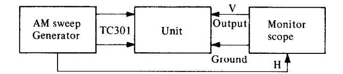
| Set signal | Adjust | Adjust for |
|---|---|---|
| 450 kHz | L305 |
The output of monitor
scope becomes maximum symmetrical response |
Remark : Usually not necessary to adjust.
2. AM RF
3. LW RF (Only T-08L)

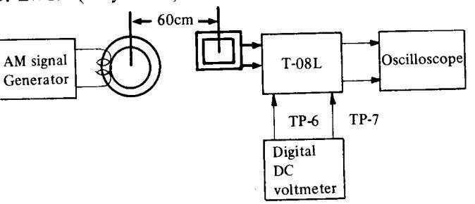
| c | ||||||||||
|---|---|---|---|---|---|---|---|---|---|---|
| Step | Set to dial | Adjust | Output indicator | Adjust for | Step | Set to dial | Adjust | Output indic | ator Adjust | ior |
| 1 | (603)kHz | L303 |
Digital |
3.7V | 1 | 164 kHz | L304 | Digital | 4.9V | ' |
| 2 |
1404
(1400) kHz |
TC303 |
DC
voltmeter |
15.5V | 2 | 317 kHz | TC304 | voltmeter | 15.8 | V |
| 3 | Repeat steris noticed. | ps 1 and 2 | until no further im | provement | 3 | Repeat ste is noticed. | ps 1 and 2 u | intil no furthe | r improvement | |
| AM Signal generator | Dial to se | t Adjust A | djust for | AM Signal generator | Dial to set | Adjust | Adjust for | |||
| 1 |
603kHz
(600) |
603kH | 7 I 301 N | laximum |
164kHz
400Hz, 30% |
164kHz | L302 | Maximum |
| 1 |
603kHz
(600) 400Hz, 30% mod. |
603kHz | L301 | Maximum |
164kHz
400Hz, 30% mod. |
164kHz | L302 | Maximum | ||
|---|---|---|---|---|---|---|---|---|---|---|
| 2 |
1404kHz
(1400) 400Hz, 30% mod. |
1404kHz | TC301 | Maximum | 2 |
317kHz
400Hz, 30% mod. |
317kHz | TC302 | Maximum | |
| 3 | Repeat step | os 1 and 2 för | maximum. | 3 | Repeat ste | ps 1 and 2 for | maximum. |
( ): 120V model
PC BOARD-PARTS LIST
FM/AM TUNER AND DIGITAL CIRCUIT PC BOARD (NARF-1427/b)
| CIRCUIT NO. | PARTS NO. | DESCRIPTION | CIRCUIT NO. | PARTS NO. | DESCRIPTION |
|---|---|---|---|---|---|
| TU001 |
Front end
240044 |
FD166U12 |
D805
D803, D804 D806, D807 |
223103
223105, 223133 or |
1N60
1S1555, DS442X or |
|
Q103
0104 |
ICs
222608 222541 |
μPC1167C2, FM IF system
LB1426 Signal strength meter |
D809–D811
D901 |
223145
223804 or 223848 |
1S2076TD
SR1K-2 or GP08B |
| Q201 |
222453
222575 or |
driver
HA1196, Stereo decoder TC4066BP or |
D902
D903 |
223979 or
223922 223862 |
RD27EB or
WZ270 WL01 |
|
Q301
Q405 |
222840661
222626 222618 |
4066B, Analogue switch
HA1197, AM radio system uPD1703C-016 Micro computer |
D904, D906
D905 |
224020
224082 |
WZ063
WZ056 |
|
Q406
Q412, Q414 |
222619
222513 or 222840111 |
μPB553AC, Prescaler
TC4011BP or 4011B NAND gate |
L101
L102 |
Transformers
233243 233244 |
NFIF-6029P
NFIF-6029S |
|
Q415
Q416 Q902 |
222840351
222740421 222780122 |
4035B, Shift register
74LS42, BCD to decimal decoder 78M12, Voltage regulator |
L305
L306 |
232077
232041 |
NMIF-6009
NIT-0509 |
| Q902 | / 8M12, Voltage regulator | Coils | |||
| Transistors | L201, L202 | 233181 | NMC-5018 | ||
| Q102 | 2211722 | 2SC1923 (R) | L301 | 232089 | NMA-3037 |
|
Q203-Q206
Q208 |
2211234 01 | 25C1815 (1) 01 |
L303
1.801 |
232084 |
NMO2018
NMC-9-1 |
| Q207 | 2211293 | 2SK68 (M), F.E.T | 2001 | 255051 | NMC-9-1 |
| Q302, Q303 | 2211254 or | 2SC1815 (Ý) or | Ceramic filters | ||
|
Q305
Q304 Q401 Q402 |
2210747
2211293 2211255 |
2SC945A (Q1)
2SK68 (M), F.E.T 2SC1815 (GR) |
X101, X103
X301 |
3010006
3010049 |
SFE10.7MA-A
CFM2-450BL |
| Q407-Q411 | 2211454 | 2SA1015 (Y) | Crystal | ||
| Q417, Q419 | 2211254 or | 2SC1815 (Y) or | X401 | 3010052 | XTL-4.5M |
| 0501 0504 | 2210747 | 2SC945A (Q1) | Conscitore | ||
|
Q301-Q304
Q801-Q803 |
2211255
2211254 or |
25C1815 (GR)
25C1815 (V) or |
C104 | 352741000 | 10. E 16V Elect |
| 0805-0807 | 2210747 | 2SC945A (01) | C104 | 352780339 | 3 3µF 50V Elect |
| Q804 | 2211255 | 2SC1815 (GR) | Č109 | 352780109 | 1µF, 50V, Elect. |
| Q901 | 2210747 | 2SC945A (Q1) | C111 | 352780229 | 2.2µF, 50V, Elect. |
| Q903 | 2201035 or | 2SD325 (E) or | C118 | 35274100 | 10µF, 16V, Elect. |
| 0004 | 2201034 | 2SD325 (D) |
C119
C120 C122 |
352733309 | 33μF, 10V, Elect. |
| Q904 | 2211254 or |
2SC1815 (Y) OF
2SC045A (O1) |
C120, C122 | 352/41009 | 10µF, 16V, Elect. |
| 0905 | 2210747 |
25C943A (Q1)
2SA1015 (V) |
C201 | 352750479 | 4 7µF 25V Elect |
| 2700 | 2211131 | 25/11010 (1) | C205. C206 | 352741009 | 10µF 16V Elect |
| Diodes | C207, C208 | 352780109 | 1µF, 50V, Elect. | ||
| D101, D103 | 223105, | 1$1555, | C209 | 352784799 | 0.47µF, 50V, Elect. |
| D201, D202 | 223133 or | DS442X or | C210 | 352780109 | 1µF, 50V, Elect. |
| D304 | 223145 |
1520/61D
VD1222 |
C211 | 352780339 | 3.3µF, 50V, Elect. |
|
D102
D203 D204 |
4000008
224129 or |
PD3 3F-B or |
C212
C215 |
352523614 | 360pF ± 5%, Styrol |
| D205, D204 | 224084 | WZ-032 | C215 | 352734709 | 47µF, 25V, Elect. |
| D301, D302 | 223136 | KV1226 | C217 | 352741009 | 10µF, 16V, Elect. |
| D303 | 4000068 | VD1222 | TC301, TC303 | 3060010 | NTC-20P09, Trimmer |
| D401D405 | 223105, | 1$1555, | C301 | 352741009 | 10µF, 16V, Elect. |
| D407 | 223133 or | DS442X or | C305 | 352741009 | 10µF, 16V, Elect. |
|
D410-D414
D415 D416 |
223145 | 181555 | C309 | 352744709 | 4 / µF, 10 V, Elect. |
| (Only W model) | 223133 or | DS442X | Č312 | 352750479 | 4.7µF, 25V, Elect |
| 223145 | 1S2076TD | C314 | 352721019 | 100µF, 6.3V. Elect. | |
| D503 | 2231031 or | 1N60 (ONK) or | C317 | 352780109 | 1µF, 50V, Elect. |
| D417 D424 | 223147 | 1N60FM | C324 | 372525114 | 510pF ± 5%, 50V, Styrol |
| D41/-D424 | 223105, |
181333,
DS442X or |
C402
C411 |
393160107 | 1µF, 35V, Tantalum |
| D504, D801 |
223135 or
223145 |
1S2076TD | 0411 | 332123319 | 550μr, 6.5 V, Elect. |
| CIRCUIT NO. | PARTS NO. | DESCRIPTION | CIRCUIT NO. | PARTS NO. | DESCRIPTION |
|---|---|---|---|---|---|
| C412 352721029 1,000μF, 6.3V C414 352741009 10μF, 16V, EI C505 352744709 47μF, 16V, EI C802 352750479 4.7μF, 25V, EI C806-C808 352784799 0.47μF, 50V, C811 352721019 100μF, 6.3V, C902 352784719 470μF, 50V, EI C803 352744719 470μF, 50V, FI C902 352784719 470μF, 50V, IE C903 352780109 1μF, 50V, EIE C905 352761029 1,000μF, 35V, IE C906, C909 352764719 470μF, 35V, IE C910 352741009 10wF, 45V, IE |
352721029
352741009 352744709 352750479 352784799 352744719 352744719 |
|
D104–D107
D205 D427–D432 D433, D434 D435 |
L.E.Ds
225048 225046 225057 225047 225046 |
SLP-252B-04, Signal
SLP-151B SR538D SLP-251B SLP-151B |
|
470μF, 50V, Elect.
1μF, 50V, Elect. 1,000μF, 35V, Elect. 470μF, 35V, Elect. 10μF, 16V, Elect. |
D437 |
Diode
223105, 223145 or 223133 |
181555,
182076TD or DS442X |
||
|
C911, C912
C914 C915 |
352721019
352764719 352763319 |
100μF, 6.3V, Elect.
470μF, 35V, Elect. 330μF, 35V, Elect. |
Switches
25035156 |
NPS-111-S120 | |
|
C916
C918, C919 |
352741009
352780109 |
10μF, 16V, Élect.
1μF, 50V, Elect. |
Bracket
27110127-1B |
Front | |
|
R127
R202 |
Resistors
5215046 5215048 |
N08HR50KBC, Semi-fixed
N08HR200KBC, Semi-fixed |
Cushion 28140300 | Fluorescent indicator tube | |
|
R216
R418-R422 R423-R429 |
5225015
49121104505 49121104507 |
i225015 N10HR10KBD, Semi-fixed i9121104505 100kΩx5, Network i9121104507 100kΩx7, Network |
Screws
831130080 |
3TTW+8P, Tapping screw | |
|
R430–R433
R811 R904 R905 R908 |
49121333504
5215047 441723304 441721514 441521024 |
33kΩx4, Network
N08HR100KBC, Semi-fixed 33Ω, 2W, Metal oxide film 150Ω, 2W, Metal oxide film 1kΩ, 1/2W, Metal oxide film |
Washer
870069 |
W10x5mm, Nylon | |
| R911 | 441528204 | 82Ω, 1/2W, Metal oxide film | NF PC BOARD (NAPL-1429) | ||
|
Radiator
27160011A |
RAD-05 | CIRCUIT NO. | PARTS NO. | DESCRIPTION | |
| Screws | PL902 |
210064A
831130080 |
250mA. 6.3W, Lamp
3TTW+8P, Tappins screw |
||
|
82113008
834130088 |
3P+8FN, Radiator, Pan head
3TTS+8B, Radiator, Tapping |
REMOTE CO | MINAL PC BOARD (NARM-1430) | ||
|
Nut
863130 |
N-3FN | CIRCUIT NO. | PARTS NO. | DESCRIPTION |
| P401 | 25050070 | NSCT-7P20 |
S201 S401
INDICATOR PC BOARD (NADIS-1428)
Switches (Only W model) 25065160 NSS-2273, De-emphasis 250142 NSS-2225, AM band
| CIRCUIT NO. | PARTS NO. | DESCRIPTION | ||
|---|---|---|---|---|
| Transistor | ||||
| Q420 | 2211254 or | 2SC1815 (Y) or | ||
| i. | 2210747 | 2SC945A (Q1) | ||
| Fluorescent in | dicator tube | |||
| Q422 | 212010 | 7-BT-05A2 | ||
1-08
PC BOARD-PARTS LIST
G model
FM/AM TUNER AND DIGITAL CIRCUIT PC BOARD (NARF-1427a)
| CIRCUIT NO. | PARTS NO. | DESCRIPTION | CIRCUIT NO. | PARTS NO. | DESCRIPTION |
|---|---|---|---|---|---|
|
Front end
240044 |
FD166U12 |
D806, D807
D805 D809–D811 |
223145
223103 223105, |
1S2076TD
1N60 1S1555, |
|
| 0102 | "PC1167C2_EM_IE_system |
223133 or
223145 |
DS442X or
1S2076TD |
||
|
Q103
Q104 |
222541 | LB1426, Signal strength meter | D901 |
223804 or
223848 |
SR1K-2 or
GP08B |
| Q201 | 222453 |
driver
HA1196, Stereo decoder |
D902 | 223979 or |
RD27EB or
WZ270 |
| Q202 |
222575 or
222840661 |
TC4066BP or
4066B, Analogue switch |
D903 | 223862 |
WL01
WZ063 |
|
Q301
O405 |
222626
222618 |
HA1197, AM radio system
µPD1703C016, Micro computer |
D904, D908
D905 |
224020 | WZ056 |
|
Q406
Q412, Q414 |
222619
222513 ог |
µPB553AC, Prescaler
TC4011BP or |
Transformers | ||
| 0415 | 222840111 | 4011B, NAND gate |
L101
L102 |
233243
233244 |
NFIF-6029P
NFIF-6029S |
|
Q415
Q416 |
222740421 | 74LS42, BCD to decimal decoder |
L305
L306 |
232077
232041 |
NMIF-6009
NIT-0509 |
| Q902 | 222/80122 | /8M12, voltage regulator | 2000 | 202011 | |
| 0101 0102 | 2211722 | 2SC1923 (B) | Coils | ||
| Q203–Q206 | 2211254 or | 2SC1815 (Y) or | L201, L202 | 233181 |
NMC-5018
NMC-6027 |
| Q208 | 2210747 |
2SC945A (Q1)
2SK68 (M) E E T |
L203 | 232089 | NMA-3037 |
| 0302 0303 |
2211255
2211254 or |
2SC1815 (Y) or | L303 | 232084 | NMO2018 |
| Q305 | 2210747 | 2SC945A (Q1) | L801 | 233031 | NMC-9-1 |
| Q304 | 2211293 | 2SK68 (M), F.E.T | Ceramic filters | ||
|
Q401, Q402
Q407-Q411 |
2211255 |
2SC1815 (GK)
2SA1015 (Y) |
X101-X103 | 3010043 | SFE10.7MA-A |
| Q417, Q419 |
2211254 or
2210747 |
2SC1815 (Y) or
2SC9454 (O1) |
X301 | 3010049 | CFM2-450BL |
| Q501-Q504 | 2211255 | 2SC1815 (GR) | ¥401 | Crystal | хті а 5 м |
|
Q801-Q803
Q805-Q807 |
2211254 or
2210747 |
2SC1815 (Y) or
2SC945A (O1) |
A401 | 3010032 | ATE 4.5M |
| Q804 | 2211255 | 2SC1815 (GR) | 0104 | Capacitors | 10.E 16V Elect |
| Q901 | 2210747 | 2SC945A (Q1) |
C104
C106 |
352741009 |
10μF, 16V, Elect.
3 3μF 50V Elect |
| Q903 | 2201035 or |
28D325 (E) or
28D325 (D) |
C100 | 352780109 | 1µF, 50V, Elect. |
| 0904 |
2201034
2211254 or |
2SC1815 (Y) or | C111 | 352780229 | 2.2µF, 50V, Elect. |
| 2210747 | 2SC945A (Q1) | C118 | 352741009 | 10µF, 16V, Elect. | |
| Q905 | 2211454 | 2SA1015 (Y) |
C119
C120 C122 |
352/33309 | 3.3µF, 10V, Elect. |
| Diodes |
C120, C122
C201 |
352742219 | 220µF, 16V, Elect. | ||
| D101, D103 | 223105 or | 1$1555 or | C202 | 352750479 | 4.7µF, 25V, Elect. |
| D201, D202 | 223133 or | DS442X or | C205, C206 | 352741009 | 10µF, 16V, Elect. |
| D304 | 223145 | 1S2076TD | C207, C208 | 352780109 | 1µF, 50V, Elect. |
| D102 · | 4000068 |
VD1222
BD2 2E B or |
C209 | 352780109 | 1µF. 50V. Elect. |
| D203, D204 | 224129 01 | WZ-032 | C211 | 352780339 | 3.3µF, 50V, Elect. |
| D301, D302 | 223136 | KV1226 | C212 | 372523614 | 360pF ± 5%, 50V, Styrol |
| D303 | 4000068 | VD1222 |
C215
C216 |
352732209 | 22µF, 23V, Elect. |
| D401-D405 | 223105, |
181333,
D84438 or |
C210 | 352741009 | 10µF, 16V, Elect. |
| D407 | 223145 | 1S2076TD | TC301, TC303 | 3060010 | NTC-20P09, Trimmer |
| D501, D502 | C301 | 352741009 | 10µF, 16V, Elect. | ||
| D503 | 2231031 or | 1N60 (ONK) or |
C305
C309 |
352741009
352744709 |
10µF, 16V, Elect.
47µF 16V Elect |
| D504 D801 | 223147 |
1NOUPM
1S1555 |
C311 | 352780339 | 3.3µF, 50V, Elect. |
| D803, D804 | 223133 or | DS442X or | C312 | 352750479 | 4.7μF, 25V, Elect. |
| CIRCUIT NO. | PARTS NO. | DESCRIPTION | CIRCUIT NO. | PARTS NO. | DESCRIPTION |
|---|---|---|---|---|---|
|
C314
C317 C324 C402 C411 C412 C414 |
352721019 100μF, 6.3V, Elect. 352780109 1μF, 50V, Elect. 372525114 510pF±5%, 50V, Styrol 395160107 1μF, 35V, Tantalum 352723319 330μF, 6.3V, Elect. 352721029 1,000μF, 6.3V, Elect. 352741009 10μF, 16V, Elect. |
D104-D107
D205 D427-D432 D433, D434 D435 |
L.E.Ds
225048 225046 225057 225047 225046 |
SLP-252B-04, Signal
SLP-151B SR538D SLP-251B SLP-151B |
|
|
C802
C806–C808 C809 C811 C902 |
352750479
352784799 352744719 352721019 352784719 |
4.7μF, 25V, Elect.
0.47μF, 50V, Elect. 470μF, 16V, Elect. 100μF, 6.3V, Elect. 470μF, 50V, Elect. |
D437 |
Diode
223105, 223145 or 223133 |
1$1555,
1$2076TD or D$442X |
|
C903
C905 C906, C909 |
352780109
352761029 352764719 |
1μF, 50V, Elect.
1,000μF, 35V, Elect. 470μF, 35V, Elect. |
Switches
25035156 |
NPS-111-S120 | |
|
C910
C911, C912 C914 |
352741009
352721019 352764719 |
10μF, 16V, Elect.
100μF, 6.3V, Elect. 470μF, 35V, Elect. |
Bracket
27110127-1B |
Front | |
|
C915
C916 C918, C919 |
352763319
352741009 352780109 |
330μF, 35V, Elect.
10μF, 16V, Elect. 1μF, 50V, Elect. |
Cushion
28140300 |
Fluorescent indicator tube | |
| R127 |
Resistors
5215046 N08HR50KBC, Semi |
N08HR50KBC, Semi-fixed |
Screws
831130080 |
3TTW+8P, Tapping screw | |
|
R202
R216 R418-R422 |
5215048
5225015 49121104505 |
N08HR200KBC, Semi-fixed
N10HR10KBD, Semi-fixed 100kΩx5, Network |
Washer
870069 |
W10×5mm, Nylon | |
|
R423-R429
R430-R433 R811 |
49121104507
49121333504 5215047 |
100ks2x7, Network
33kΩx4, Network N08HR100KBC, Semi-fixed |
MP PC BOARD (NAPL-1429) | ||
|
R904
R905 |
441723304
441721514 |
33Ω, 2W, Metal oxide film
150Ω, 2W, Metal oxide film |
CIRCUIT NO. | PARTS NO. | DESCRIPTION |
|
R908
R911 |
441521024
441528204 |
1kΩ, 1/2W, Metal oxide film
82Ω, 1/2W, Metal oxide film |
PL902 |
210064A
831130080 |
250mA, 6.3V, Lamp
3TTW+8P, Tapping screw |
|
Radiator
27160011A |
RAD-05 | ||||
| Screws | REMOTE CO | INTROL IERN | MINAL PC BOARD (NARM-1430) | ||
| 82113008 | 3P+8FN, Radiator | CIRCUIT NO. | PARTS NO. | DESCRIPTION | |
| 834140088 | 3TTS+8B, Radiator | P401 | 25050070 | NSCT-7P20 | |
|
Nut
863130 |
N-3FN | ||||
| INDICATOR | PC BOARD (N | IADIS-1428a) | |||
| CIRCUIT NO. | PARTS NO. | DESCRIPTION | |||
| Transistors |
| Transistors | |||
|---|---|---|---|
| Q420 | 2211254 or | 2SC1815 (Y) or | |
| - | 2210747 | 2SC945A (Q1) | |
| Q421 | 2211255 | 2SC1815 (GR) | |
| 1 10010000111 | ||
|---|---|---|
| Q422 | 212010 | 7-BT-05A2 |
PC BOARD-PARTS LIST
T-08L
FM/AM TUNER AND DIGITAL CIRCUIT PC BOARD (NARF-1427c)
| CIRCUIT NO. | PARTS NO. | DESCRIPTION | CIRCUIT NO. | PARTS NO. | DESCRIPTION |
|---|---|---|---|---|---|
| TU001 |
Front end
240044 |
FD166U12 |
D806, D807
D805 D809–D811 |
223145
223103 223105, |
1S2076TD
1N60 1S1555, |
| ICs | 223133 or | DS442X or | |||
|
Q103
Q104 |
222608 |
µPC1167C2, FM IF system
I B1426 Signal meter driver |
D901 | 223804 or | SR1K-2 or |
| Q201 | 222453 | HA1196, Stereo decoder | D003 | 223848 |
GP08B
RD27FB or |
| Q202 |
222575 or
222840661 |
TC4066BP or
4066B Analogue switch |
D902 | 223922 | WZ270 |
| Q301 | 222626 | HA1197, AM radio system | D903 | 223862 |
WL01
WZ063 |
|
Q405
Q406 |
222618
222619 |
µPD1703C-016, Micro computer
µPB553AC Prescaler |
D904, D900
D905 |
224020 | WZ056 |
| Q412-Q414 | 222513 or | TC4011BP or | Transformers | ||
| 0415 |
222840111
222840351 |
4011B, NAND gate
4035B. Shift register |
L101 | 233243 | NFIF-6029P |
| Q416 | 222740421 | 74LS42, BCD to decimal decoder |
L102
L305 |
233244 |
NF1F-6029S
NM1F-6009 |
| Q902 | 222780122 | 78M12, Voltage regulator | L306 | 232041 | NIT-0509 |
| 0.1.00 | Transistors | , | |||
|
Q102
Q203-Q206 |
2211/22
2211254 or |
2SC1923 (R)
2SC1815 (Y) or |
Coils | ||
| Q208 | 2210747 | 2SC945A (Q1) | L201, L202 | 233181 |
NMC-5018
NMC 6027 |
|
Q207
Q302, Q303 |
2211293
2211254 or |
2SK68 (M), F.E.1
2SC1815 (Y) or |
L203
L301 |
232089 |
NMC-8027
NMA-3037 |
| Q305-Q310 | 2210747 | 2SC945A (Q1) | L302 | 232092 | NLA-2039 |
|
Q304
Q401-Q404 |
2211293 |
2SK68 (M), F.E.1
2SC1815 (GR) |
L303
L304 |
232084 | NLO-3015 |
| Q407-Q411 | 2211454 | 2SA1015 (Y) | L801 | 233031 | NMC-9-1 |
| Q417-Q419 | 2211254 01 |
2SC1815 (Y) or
2SC945A (Q1) |
Ceramic filters | ||
| Q501-Q504 | 2211255 | 2SC1815 (GR) | X101, X103 | 3010006 |
SFE10.7MA-A
CFM2-450 BL |
|
Q801–Q803
Q805–Q807 |
2210747 | 2SC945A (Q1) | A501 | Crustel | |
| Q804 | 2211255 |
2SC1815 (GR)
2SC9454 (O1) |
X401 | 3010052 | XTL-4.5M |
| Q903 | 2201035 or | 2SD325 (E) or | Canacitors | ||
| 0904 |
2201034
2211254 or |
2SD325 (D)
2SC1815 (Y) or |
C104 | 352741009 | 10µF, 16V, Elect. |
| 2210747 | 2SC945A (Q1) | C106 | 352780339 | 3.3µF, 50V, Elect. | |
| Q905 | 2211454 | 2SA1015 (Y) |
C109
C111 |
352780109 |
1µF, 50V, Elect.
2.2µF, 50V, Elect. |
| D101 D102 | Diodes | 101666 | C118 | 352741009 | 10µF, 16V, Elect. |
|
D101, D103
D201, D202 |
223105
223133 or |
181858
DS442X or |
C120, C122 | 352741009 |
3.3μF, 10V, Elect.
10μF, 16V, Elect. |
| D304, D306 | 223145 | 1$2076TD | C201 | 352742219 | 220µF, 16V, Elect. |
|
D102
D203. D204 |
4000068
224129 or |
RD3.3E-B or |
C202
C205, C206 |
352741009 |
4./μF, 25 V, Elect.
10μF, 16V, Elect. |
| D201 D202 | 224084 | WZ-032 | C207, C208 | 352780109 | 1µF, 50V, Elect. |
|
D301, D302
D303 |
4000068 | VD1222 |
C209
C210 |
352780109 | 1µF, 50V, Elect. |
| D305, D311 | 223136 | KV1226 |
C211
C212 |
352780339 | 3.3µF, 50V, Elect. |
| D309, D310 | 223105, | 1$1555, | C215 | 352752209 | 22μF, 25V, Elect. |
| D401-D424 |
223133 or
223145 |
DS442X or
1S2076TD |
C216
C217 |
352734709 | 47µF, 16V, Elect. |
| D503 | 2231031 or | 1N60 (ONK) or | ТС301-ТС303 | 3060010 | NTC-20P09, Trimmer |
| D504, D801 |
223147
223105 |
1N60FM
1S1555 |
TC304
C301 |
3060011
352741009 |
NTC-45P10, Trimmer
10µF, 16V, Elect. |
| D803, D804 | 223133 or | DS442X or | Č305 | 352741009 | 10µF, 16V, Elect. |
| CIRCUIT NO. | PARTS NO. | DESCRIPTION | |||
|---|---|---|---|---|---|
| C309 | 352744709 | 47µF, 16V, Elect. | INDICATOR | PC BOARD (N | ADIS-1428b) |
|
C312
C314 |
352750479 |
4.7μF, 25V, Elect.
100μF, 6.3V, Elect. |
CIRCUIT NO. | PARTS NO. | DESCRIPTION |
|
C317
C324 C320 |
352780109
372525114 |
1μF, 50V, Elect.
510pF ± 5%, 50V, Styrol 220pF ± 5% 50V Styrol |
Q420, Q421 |
Transistors
2211254 or |
2SC1815 (Y) or |
|
C330
C331, C332 |
352784799 | 0.47µF, 50V, Elect. | 2210747 | 2SC945A (Q1) | |
|
C402
C406 |
395164797 |
0.47µF, 35V, Tantalum
330µF 6 3V Elect |
Q422 | 212010 | 7-BT-05A2 |
|
C411
C412 C414 |
352721029 | 1,000µF, 6.3V, Elect. | L.E.Ds | ||
|
C505
C802 |
352741009
352744709 352750479 |
47μF, 16V, Elect.
4.7μF, 25V, Elect. |
D104–D107
D205, D435 D427–D432 |
225048
225046 225057 |
SLP-252B-04, Signal
SLP-151B SR538D |
|
C806-C808
C809 |
352784799
352744719 |
0.47µF, 50V, Elect.
470µF, 16V, Elect. |
D433-D434 | 225047 | SLP-251B |
|
C902
C903 C905 |
352721019
352784719 352780109 352761029 |
470μF, 50V, Elect.
1μF, 50V, Elect. 1,000μF, 35V, Elect. |
D437 |
223105,
223145 or 223133 |
1S1555,
1S2076TD or DS442X |
|
C906, C909
C910 |
352764719
352741009 |
470μF, 35V, Elect.
10μF, 16V, Elect. |
D425, D426 | 223106 | 1$1554 |
|
C911, C912
C914 C915 |
352764719
352763319 |
100μF, 6.3V, Elect.
470μF, 35V, Elect. 330μF, 35V, Elect. |
Switches
25035156 |
NPS-111-S120 | |
|
C916
C918, C919 |
352741009
352780109 |
10μF, 16V, Elect.
1μF, 50V, Elect. |
Bracket
27110127-1B |
Front | |
|
R127
R202 |
Resistors
5215046 5215048 |
N08HR50KBC, Semi-fixed
N08HR200KBC, Semi-fixed |
Cushion 28140300 | Fluorescent indicator tube | |
|
R216
R418–R422 R423–R429 |
5225015
49121104505 49121104507 |
N10HR10KBD, Semi-fixed
100kΩx5, Network 100kΩx7, Network |
Screws
831130080 |
3TTW+8P, Tapping screw | |
|
R430-R433
R811 R904 R905 |
49121333504
5215047 441723304 441721514 |
33kΩx4, Network
N08HR100KBC, Semi-fixed 33Ω, 2W, Metal oxdie film 150Ω, 2W, Metal oxide film |
Washer
870069 |
W10x5mm, Nylon | |
|
R908
R911 |
441521024
441528204 |
1kΩ, 1/2W, Metal oxide film
82Ω, 1/2W, Metal oxide film |
DIAL ILLUN | INATION LAI | MP PC BOARD (NAPL-1429) |
| Relaies | CIRCUIT NO. | PARTS NO. | DESCRIPTION | ||
|
RL301
RL302 |
25065135
25065093 |
FRL-644D05-2AS
FRL-644D12-1AS |
PL902 |
210064A
831130080 |
250mA, 6.3V, Lamp
3TTW+8P, Tapping screw |
|
Radiator
27160011A |
RAD-05 | D436 | 225046 | SLP-151B, L.E.D | |
| Screws | REMOTE CC | NTROL TERM | /INAL PC BOARD (NARM-1430) | ||
|
82113008
834140088 |
3P+8FN, Radiator
3TTS+8B, Radiator |
CIRCUIT NO. | PARTS NO. | DESCRIPTION | |
|
Nut
863130 |
N-3FN | P401 | 25050070 | NSCT-7P20 |
SCHEMATIC DIAGRAM
D model
BLOCK DIAGRAM
| REF. NO. | PARTS NO. | DESCRIPTION | REF. NO. | PARTS NO. | DESCRIPTION |
|---|---|---|---|---|---|
|
1
2 3 4 |
29050566
29050567 282301 29090533C 29090532A |
Master carton box (T-08)
Master carton box (T-08L) Sealing hook Pad, right Pad, left |
(220V model)
29340621 292064A 29100006 |
Instruction manual
FM antenna 350x250mm, Poly-vinyl bag |
|
| 5 | 29100051 | 420x750mm, Poly-vinyl bag | (West Germany | / model) | |
|
6
7 |
260012
(U.S.A. model) 29340620 |
50x450mm, Damplon tape
Accessary bag ass'y Instruction manual FM antenna Two batteries Service station list 350x250mm, Poly-vinyl bag Warranty card |
29340621
292064A 29100006 29365005-3 |
Instruction manual
FM antenna 350x250mm, Poly-vinyl bag Warranty card |
|
| 292064A | (Universal model) | ||||
|
3010054
29358002 29100006 29365006-3 |
29340621
292064A 29100006 25055040 |
Instruction manual
FM antenna 350x250mm, Poly-vinyl bag Conversion plug |
|||
| (120V model) | |||||
| 29340620 | Instruction manual | ||||
ONKYO CORPORATION
FM antenna
Two batteries 350x250mm, Poly-vinyl bag
292064A
3010054 29100006
International Division: No. 24 Mori Bldg., 23-5, 3-chome, Nishi-Shinbashi, Minato-ku, Tokyo, Japan Telex: 2423551 ONKYO J. Phone: 03-432-6981 ONKYO U.S.A. CORPORATION Eastern Office: 200 Williams Drive, Ramsey, N.J. 07446 Tel. 201-825-7950 Midwest Office: 2406 Martin Lane Rolling Meadows, III 60008 Tel. 312-577-4300 Western Office: 8607 Canoga Ave., Canoga Park, CA, 91304 Tel. 213-341-8114 ONKYO DEUTSCHLAND GMBH, ELECTRONICS 8034 München-Germering, Industriestrasse 18, West Germany. Telex: 521726 Telefon: (089)-84-3071


 Loading...