

Page 1
Cat. No. W197-E1-2B
SYSMAC mini
SP10/SP16/SP20
Programmable Controller
Page 2
SYSMAC mini Programmable Controllers
SP10/SP16/SP20
Operation Manual
Revised September 1997
Page 3

Notice:
OMRON products are manufactured for use according to proper procedures by a qualified operator
and only for the purposes described in this manual.
The following conventions are used to indicate and classify precautions in this manual. Always heed
the information provided with them. Failure to heed precautions can result in injury to people or damage to the product.
DANGER Indicates information that, if not heeded, is likely to result in loss of life or serious injury.
!
WARNING Indicates information that, if not heeded, could possibly result in loss of life or serious injury .
!
Caution Indicates information that, if not heeded, could result in relatively serious or minor injury, dam-
!
age to the product, or faulty operation.
OMRON Product References
All OMRON products are capitalized in this manual. The word “Unit” is also capitalized when it refers
to an OMRON product, regardless of whether or not it appears in the proper name of the product.
The abbreviation “Ch,” which appears in some displays and on some OMRON products, often means
“word” and is abbreviated “Wd” in documentation in this sense.
The abbreviation “PC” means Programmable Controller and is not used as an abbreviation for anything else.
Visual Aids
The following headings appear in the left column of the manual to help you locate different types of
information.
OMRON, 1991
All rights reserved. No part of this publication may be reproduced, stored in a retrieval system, or transmitted, in any
form, or by any means, mechanical, electronic, photocopying, recording, or otherwise, without the prior written permission of OMRON.
No patent liability is assumed with respect to the use of the information contained herein. Moreover, because OMRON is
constantly striving to improve its high–quality products, the information contained in this manual is subject to change
without notice. Every precaution has been taken in the preparation of this manual. Nevertheless, OMRON assumes no
responsibility for errors or omissions. Neither is any liability assumed for damages resulting from the use of the information contained in this publication.
Note Indicates information of particular interest for efficient and convenient operation
of the product.
1, 2, 3...
1. Indicates lists of one sort or another, such as procedures, checklists, etc.
ii
Page 4

About this Manual:
This manual describes the installation and operation of the SYSMAC mini Programmable Controllers
and includes the sections described below. The SYSMAC mini PCs include the SP10, SP16, and the
SP20 and are called SP-series PCs in this manual. Please read this manual completely and be sure
you understand the information provide before attempting to install and operation any of the SP-series PCs.
Section 1 Introduction
gramming. It also provides an overview of the process of programming and operating a PC and
explains basic terminology used with OMRON PCs. Descriptions of the features of the SP-series PCs
and Units that comprise SP-series systems are also provided.
Section 2 Installation
dimensions of all components are also presented.
Section 3 Programming
five subsections provide enough information to enable you to write, input, and execute a basic ladderdiagram program. The remainder of this section provides more advanced programming information,
3–7
with
Section 4 Operation
Console, such as monitoring, data modification, and Memory Card operations.
Section 5 Troubleshooting
also necessary when debugging a program.
The appendices provide tables of standard OMRON products available for the SP-series PCs, specifi-
cations, reference tables of instructions and Programming Console operations, and error and arithmetic flag operation. Also provided are several programming and data area assignment sheets that can
be copied out of the manual and used in developing programs.
describing individually each instruction in the SP-series instruction set.
explains the background and some of the terms used in ladder-diagram pro-
provides details on the installation environment and the wiring of the PC. The
describes information necessary for programming SP-series PCs. The first
provides further information on operating SP-series PCs via the Programming
provides information on error indications. Information in this section is
!
WARNING Failure to read and understand the information provided in this manual may result in personal
injury or death, damage to the product, or product failure. Please read each section in its
entirety and be sure you understand the information provided in the section and related
sections before attempting any of the procedures or operations given.
iii
Page 5

TABLE OF CONTENTS
PRECAUTIONS ix . . . . . . . . . . . . . . . . . . . . . . . . . . . . . . . . . . . . . . . . . . . . . . . .
1 Intended Audience x . . . . . . . . . . . . . . . . . . . . . . . . . . . . . . . . . . . . . . . . . . . . . . . .
2 General Precautions x . . . . . . . . . . . . . . . . . . . . . . . . . . . . . . . . . . . . . . . . . . . . . . .
3 Safety Precautions x . . . . . . . . . . . . . . . . . . . . . . . . . . . . . . . . . . . . . . . . . . . . . . . .
4 Operating Environment Precautions x . . . . . . . . . . . . . . . . . . . . . . . . . . . . . . . . . . .
5 Application Precautions xi . . . . . . . . . . . . . . . . . . . . . . . . . . . . . . . . . . . . . . . . . . . .
SECTION 1 – Introduction 1 . . . . . . . . . . . . . . . . . . . . . . . . . . . . . . . . . . . . . . .
1-1 Features 2 . . . . . . . . . . . . . . . . . . . . . . . . . . . . . . . . . . . . . . . . . . . . . . . . . . . . . . . . .
1-2 PC Basics 2 . . . . . . . . . . . . . . . . . . . . . . . . . . . . . . . . . . . . . . . . . . . . . . . . . . . . . . .
1-2-1 PC Terminology 3 . . . . . . . . . . . . . . . . . . . . . . . . . . . . . . . . . . . . . . . . . .
1-2-2 Overview of PC Operation 4 . . . . . . . . . . . . . . . . . . . . . . . . . . . . . . . . .
1-3 Units 5 . . . . . . . . . . . . . . . . . . . . . . . . . . . . . . . . . . . . . . . . . . . . . . . . . . . . . . . . . . .
1-3-1 CPU 5 . . . . . . . . . . . . . . . . . . . . . . . . . . . . . . . . . . . . . . . . . . . . . . . . . . .
1-3-2 Programming Console 6 . . . . . . . . . . . . . . . . . . . . . . . . . . . . . . . . . . . . .
1-3-3 Link Adapter 7 . . . . . . . . . . . . . . . . . . . . . . . . . . . . . . . . . . . . . . . . . . . .
1-3-4 Memory Cards 7 . . . . . . . . . . . . . . . . . . . . . . . . . . . . . . . . . . . . . . . . . . .
1-4 PC Configuration 8 . . . . . . . . . . . . . . . . . . . . . . . . . . . . . . . . . . . . . . . . . . . . . . . . .
1-4-1 Basic Configuration 8 . . . . . . . . . . . . . . . . . . . . . . . . . . . . . . . . . . . . . . .
1-4-2 Expanded System Configuration: PC Links 8 . . . . . . . . . . . . . . . . . . . .
SECTION 2 – Installation 11 . . . . . . . . . . . . . . . . . . . . . . . . . . . . . . . . . . . . . . . .
2-1 Dimensions 12 . . . . . . . . . . . . . . . . . . . . . . . . . . . . . . . . . . . . . . . . . . . . . . . . . . . . . .
2-2 Installation 13 . . . . . . . . . . . . . . . . . . . . . . . . . . . . . . . . . . . . . . . . . . . . . . . . . . . . . .
2-2-1 Installation Environment 13 . . . . . . . . . . . . . . . . . . . . . . . . . . . . . . . . . . .
2-2-2 Cooling 14 . . . . . . . . . . . . . . . . . . . . . . . . . . . . . . . . . . . . . . . . . . . . . . . . .
2-2-3 Preventing Noise 14 . . . . . . . . . . . . . . . . . . . . . . . . . . . . . . . . . . . . . . . . .
2-2-4 Mounting Requirements 15 . . . . . . . . . . . . . . . . . . . . . . . . . . . . . . . . . . .
2-3 Wiring 15 . . . . . . . . . . . . . . . . . . . . . . . . . . . . . . . . . . . . . . . . . . . . . . . . . . . . . . . . . .
2-3-1 Power Supply 15 . . . . . . . . . . . . . . . . . . . . . . . . . . . . . . . . . . . . . . . . . . . .
2-3-2 I/O Connections 16 . . . . . . . . . . . . . . . . . . . . . . . . . . . . . . . . . . . . . . . . . .
2-3-3 Precautions 20 . . . . . . . . . . . . . . . . . . . . . . . . . . . . . . . . . . . . . . . . . . . . . .
2-4 Programming Console 20 . . . . . . . . . . . . . . . . . . . . . . . . . . . . . . . . . . . . . . . . . . . . .
2-4-1 Designating the PC 21 . . . . . . . . . . . . . . . . . . . . . . . . . . . . . . . . . . . . . . .
2-4-2 Input Filters 22 . . . . . . . . . . . . . . . . . . . . . . . . . . . . . . . . . . . . . . . . . . . . .
SECTION 3 – Programming 25 . . . . . . . . . . . . . . . . . . . . . . . . . . . . . . . . . . . . . .
3-1 Introduction 27 . . . . . . . . . . . . . . . . . . . . . . . . . . . . . . . . . . . . . . . . . . . . . . . . . . . . . .
3-2 Memory Areas 27 . . . . . . . . . . . . . . . . . . . . . . . . . . . . . . . . . . . . . . . . . . . . . . . . . . .
3-2-1 Data Area Structure 28 . . . . . . . . . . . . . . . . . . . . . . . . . . . . . . . . . . . . . . .
3-2-2 I/O Bits 30 . . . . . . . . . . . . . . . . . . . . . . . . . . . . . . . . . . . . . . . . . . . . . . . . .
3-2-3 Work Bits 31 . . . . . . . . . . . . . . . . . . . . . . . . . . . . . . . . . . . . . . . . . . . . . . .
3-2-4 Dedicated Bits 31 . . . . . . . . . . . . . . . . . . . . . . . . . . . . . . . . . . . . . . . . . . .
3-2-5 LR Area 33 . . . . . . . . . . . . . . . . . . . . . . . . . . . . . . . . . . . . . . . . . . . . . . . .
3-2-6 DR Area 36 . . . . . . . . . . . . . . . . . . . . . . . . . . . . . . . . . . . . . . . . . . . . . . . .
3-2-7 TC (Timer/Counter) Area 36 . . . . . . . . . . . . . . . . . . . . . . . . . . . . . . . . . .
3-3 The Programming Console 37 . . . . . . . . . . . . . . . . . . . . . . . . . . . . . . . . . . . . . . . . . .
3-3-1 The Keyboard 38 . . . . . . . . . . . . . . . . . . . . . . . . . . . . . . . . . . . . . . . . . . .
3-3-2 PC Modes 39 . . . . . . . . . . . . . . . . . . . . . . . . . . . . . . . . . . . . . . . . . . . . . . .
v
Page 6

Table of contents
3-4 Basic Programming 39 . . . . . . . . . . . . . . . . . . . . . . . . . . . . . . . . . . . . . . . . . . . . . . .
3-4-1 Terminology 39 . . . . . . . . . . . . . . . . . . . . . . . . . . . . . . . . . . . . . . . . . . . . .
3-4-2 Mnemonic Code 41 . . . . . . . . . . . . . . . . . . . . . . . . . . . . . . . . . . . . . . . . . .
3-4-3 Ladder Instructions 42 . . . . . . . . . . . . . . . . . . . . . . . . . . . . . . . . . . . . . . .
3-4-4 OUTPUT and OUTPUT NOT 44 . . . . . . . . . . . . . . . . . . . . . . . . . . . . . . .
3-4-5 The END Instruction 44 . . . . . . . . . . . . . . . . . . . . . . . . . . . . . . . . . . . . . .
3-4-6 Logic Block Instructions 45 . . . . . . . . . . . . . . . . . . . . . . . . . . . . . . . . . . .
3-4-7 Coding Multiple Right-hand Instructions 51 . . . . . . . . . . . . . . . . . . . . . .
3-5 Inputting the Program 51 . . . . . . . . . . . . . . . . . . . . . . . . . . . . . . . . . . . . . . . . . . . . . .
3-5-1 Initial Programming Console Operation 51 . . . . . . . . . . . . . . . . . . . . . . .
3-5-2 Designating the PC 52 . . . . . . . . . . . . . . . . . . . . . . . . . . . . . . . . . . . . . . .
3-5-3 Clearing Memory 53 . . . . . . . . . . . . . . . . . . . . . . . . . . . . . . . . . . . . . . . . .
3-5-4 Clearing Error Messages 54 . . . . . . . . . . . . . . . . . . . . . . . . . . . . . . . . . . .
3-5-5 Setting and Reading from Program Memory Address 54 . . . . . . . . . . . .
3-5-6 Entering or Editing Programs 55 . . . . . . . . . . . . . . . . . . . . . . . . . . . . . . .
3-5-7 Checking the Program 57 . . . . . . . . . . . . . . . . . . . . . . . . . . . . . . . . . . . . .
3-5-8 Program Transfer 58 . . . . . . . . . . . . . . . . . . . . . . . . . . . . . . . . . . . . . . . . .
3-5-9 Program Searches 61 . . . . . . . . . . . . . . . . . . . . . . . . . . . . . . . . . . . . . . . .
3-5-10 Inserting and Deleting Instructions 61 . . . . . . . . . . . . . . . . . . . . . . . . . . .
3-6 Advanced Programming 64 . . . . . . . . . . . . . . . . . . . . . . . . . . . . . . . . . . . . . . . . . . . .
3-6-1 Interlocks 64 . . . . . . . . . . . . . . . . . . . . . . . . . . . . . . . . . . . . . . . . . . . . . . .
3-6-2 Controlling Bit Status 65 . . . . . . . . . . . . . . . . . . . . . . . . . . . . . . . . . . . . .
3-6-3 DIFFERENTIATE UP and DIFFERENTIATE DOWN 66 . . . . . . . . . . .
3-6-4 KEEP 66 . . . . . . . . . . . . . . . . . . . . . . . . . . . . . . . . . . . . . . . . . . . . . . . . . .
3-6-5 Self-maintaining Bits (Seal) 67 . . . . . . . . . . . . . . . . . . . . . . . . . . . . . . . .
3-6-6 Work Bits (Internal Relays) 67 . . . . . . . . . . . . . . . . . . . . . . . . . . . . . . . . .
3-6-7 Programming Precautions 69 . . . . . . . . . . . . . . . . . . . . . . . . . . . . . . . . . .
3-7 Instruction Set 71 . . . . . . . . . . . . . . . . . . . . . . . . . . . . . . . . . . . . . . . . . . . . . . . . . . . .
3-7-1 Notation 71 . . . . . . . . . . . . . . . . . . . . . . . . . . . . . . . . . . . . . . . . . . . . . . . .
3-7-2 Instruction Format 71 . . . . . . . . . . . . . . . . . . . . . . . . . . . . . . . . . . . . . . . .
3-7-3 Data Areas, Definer Values, and Flags 71 . . . . . . . . . . . . . . . . . . . . . . . .
3-7-4 Coding Right-hand Instructions 72 . . . . . . . . . . . . . . . . . . . . . . . . . . . . . .
3-7-5 LOAD, LOAD NOT, AND, AND NOT, OR, and OR NOT 74 . . . . . . . .
3-7-6 AND LOAD and OR LOAD 75 . . . . . . . . . . . . . . . . . . . . . . . . . . . . . . . .
3-7-7 OUTPUT and OUTPUT NOT - OUT and OUT NOT 75 . . . . . . . . . . . .
3-7-8 DIFFERENTIATE UP and DIFFERENTIATE DOWN -
3-7-9 KEEP - KEEP(12) 78 . . . . . . . . . . . . . . . . . . . . . . . . . . . . . . . . . . . . . . . .
3-7-10 INTERLOCK and INTERLOCK CLEAR - IL(02) and ILC(03) 79 . . . .
3-7-11 END - END(01) 81 . . . . . . . . . . . . . . . . . . . . . . . . . . . . . . . . . . . . . . . . . .
3-7-12 NO OPERATION - NOP(00) 81 . . . . . . . . . . . . . . . . . . . . . . . . . . . . . . . .
3-7-13 Timers and Counters 81 . . . . . . . . . . . . . . . . . . . . . . . . . . . . . . . . . . . . . .
3-7-14 TIMER - TIM 83 . . . . . . . . . . . . . . . . . . . . . . . . . . . . . . . . . . . . . . . . . . .
3-7-15 TIMER - TIMM(20) 86 . . . . . . . . . . . . . . . . . . . . . . . . . . . . . . . . . . . . . .
3-7-16 HIGH-SPEED TIMER - TIMH(21) 87 . . . . . . . . . . . . . . . . . . . . . . . . . .
3-7-17 ANALOG TIMER - ATIM(22) 87 . . . . . . . . . . . . . . . . . . . . . . . . . . . . . .
3-7-18 ANALOG TIMER 1 and 2 - ATM1(25) and ATM2(26) 88 . . . . . . . . . . .
3-7-19 COUNTER - CNT 89 . . . . . . . . . . . . . . . . . . . . . . . . . . . . . . . . . . . . . . . .
3-7-20 REVERSIBLE DRUM COUNTER -RDM(23) 92 . . . . . . . . . . . . . . . . .
3-7-21 HIGH-SPEED COUNTER - CNTH(24) 94 . . . . . . . . . . . . . . . . . . . . . . .
3-7-22 SHIFT REGISTER - SFT(33) 96 . . . . . . . . . . . . . . . . . . . . . . . . . . . . . . .
3-7-23 MOVE - MOV(30) 98 . . . . . . . . . . . . . . . . . . . . . . . . . . . . . . . . . . . . . . . .
3-7-24 MOVE NOT - MVN(31) 98 . . . . . . . . . . . . . . . . . . . . . . . . . . . . . . . . . . .
3-7-25 COMPARE - CMP(32) 99 . . . . . . . . . . . . . . . . . . . . . . . . . . . . . . . . . . . .
3-7-26 BLOCK COMPARE - BCMP(34) 101 . . . . . . . . . . . . . . . . . . . . . . . . . . . .
3-7-27 CLEAR CARRY - CLC(44) 102 . . . . . . . . . . . . . . . . . . . . . . . . . . . . . . . .
DIFU(10) and DIFD(11) 76 . . . . . . . . . . . . . . . . . . . . . . . . . . . . . . . . . . .
vi
Page 7

Table of contents
3-7-28 BCD ADD - ADD(40) 102 . . . . . . . . . . . . . . . . . . . . . . . . . . . . . . . . . . . . .
3-7-29 BCD SUBTRACT - SUB(41) 103 . . . . . . . . . . . . . . . . . . . . . . . . . . . . . . .
3-7-30 AND WORD- ANDW(42) 105 . . . . . . . . . . . . . . . . . . . . . . . . . . . . . . . . .
3-7-31 OR WORD - ORW(43) 105 . . . . . . . . . . . . . . . . . . . . . . . . . . . . . . . . . . . .
3-7-32 STEP DEFINE and STEP START-STEP(04)/SNXT(05) 106 . . . . . . . . . .
3-8 Debugging 109 . . . . . . . . . . . . . . . . . . . . . . . . . . . . . . . . . . . . . . . . . . . . . . . . . . . . . . .
3-8-1 Displaying and Clearing Error Messages 109 . . . . . . . . . . . . . . . . . . . . . .
3-8-2 Reading the Scan Time 110 . . . . . . . . . . . . . . . . . . . . . . . . . . . . . . . . . . . .
3-9 Program Execution 110 . . . . . . . . . . . . . . . . . . . . . . . . . . . . . . . . . . . . . . . . . . . . . . . .
3-9-1 Scan 110 . . . . . . . . . . . . . . . . . . . . . . . . . . . . . . . . . . . . . . . . . . . . . . . . . . .
3-10 I/O Response Time 111 . . . . . . . . . . . . . . . . . . . . . . . . . . . . . . . . . . . . . . . . . . . . . . . .
3-10-1 Single PCs 112 . . . . . . . . . . . . . . . . . . . . . . . . . . . . . . . . . . . . . . . . . . . . . .
3-10-2 Multiple PCs 113 . . . . . . . . . . . . . . . . . . . . . . . . . . . . . . . . . . . . . . . . . . . .
SECTION 4 – Operation 115 . . . . . . . . . . . . . . . . . . . . . . . . . . . . . . . . . . . . . . . . .
4-1 Monitoring Operation and Modifying Data 116 . . . . . . . . . . . . . . . . . . . . . . . . . . . . .
4-1-1 Bit/Multibit Monitor 116 . . . . . . . . . . . . . . . . . . . . . . . . . . . . . . . . . . . . . .
4-1-2 Force Set/Reset 119 . . . . . . . . . . . . . . . . . . . . . . . . . . . . . . . . . . . . . . . . . .
4-1-3 Hexadecimal/BCD Data Modification 120 . . . . . . . . . . . . . . . . . . . . . . . .
4-1-4 Binary Monitor 121 . . . . . . . . . . . . . . . . . . . . . . . . . . . . . . . . . . . . . . . . . .
4-1-5 Binary Data Modification 122 . . . . . . . . . . . . . . . . . . . . . . . . . . . . . . . . . .
4-2 Memory Card Initialization 123 . . . . . . . . . . . . . . . . . . . . . . . . . . . . . . . . . . . . . . . . .
SECTION 5 – Troubleshooting 127 . . . . . . . . . . . . . . . . . . . . . . . . . . . . . . . . . . . .
5-1 Alarm Indicators 128 . . . . . . . . . . . . . . . . . . . . . . . . . . . . . . . . . . . . . . . . . . . . . . . . . .
5-2 Reading and Clearing Errors and Messages 128 . . . . . . . . . . . . . . . . . . . . . . . . . . . . .
5-3 Error Messages 128 . . . . . . . . . . . . . . . . . . . . . . . . . . . . . . . . . . . . . . . . . . . . . . . . . . .
5-4 Error Flags 129 . . . . . . . . . . . . . . . . . . . . . . . . . . . . . . . . . . . . . . . . . . . . . . . . . . . . . .
Appendix 131 . . . . . . . . . . . . . . . . . . . . . . . . . . . . . . . . . . . . . . . . . . . . . . . . . . . . . .
A – Standard Models 131 . . . . . . . . . . . . . . . . . . . . . . . . . . . . . . . . . . . . . . . . . . . . . . . . . . . .
B – Specifications 133 . . . . . . . . . . . . . . . . . . . . . . . . . . . . . . . . . . . . . . . . . . . . . . . . . . . . . .
C – Programming Instructions and Execution Times 135 . . . . . . . . . . . . . . . . . . . . . . . . . . .
D – Programming Console Operations 143 . . . . . . . . . . . . . . . . . . . . . . . . . . . . . . . . . . . . . .
E – Error and Arithmetic Flag Operation 147 . . . . . . . . . . . . . . . . . . . . . . . . . . . . . . . . . . . .
F – I/O Assignment Sheets 149 . . . . . . . . . . . . . . . . . . . . . . . . . . . . . . . . . . . . . . . . . . . . . . .
G – Program Coding Sheet 155 . . . . . . . . . . . . . . . . . . . . . . . . . . . . . . . . . . . . . . . . . . . . . . .
Glossary 161 . . . . . . . . . . . . . . . . . . . . . . . . . . . . . . . . . . . . . . . . . . . . . . . . . . . . . . .
Index 171 . . . . . . . . . . . . . . . . . . . . . . . . . . . . . . . . . . . . . . . . . . . . . . . . . . . . . . . . .
vii
Page 8

PRECAUTIONS
This section provides general precautions for using the Programmable Controller (PC) and related devices.
The information contained in this section is important for the safe and reliable application of the PC. You must read
this section and understand the information contained before attempting to set up or operate a PC system.
1 Intended Audience x . . . . . . . . . . . . . . . . . . . . . . . . . . . . . . . . . . . . . . . . . . . . . . . . .
2 General Precautions x . . . . . . . . . . . . . . . . . . . . . . . . . . . . . . . . . . . . . . . . . . . . . . . .
3 Safety Precautions x . . . . . . . . . . . . . . . . . . . . . . . . . . . . . . . . . . . . . . . . . . . . . . . . .
4 Operating Environment Precautions x . . . . . . . . . . . . . . . . . . . . . . . . . . . . . . . . . . .
5 Application Precautions xi . . . . . . . . . . . . . . . . . . . . . . . . . . . . . . . . . . . . . . . . . . . . .
ix
Page 9

Operating Environment Precautions
1 Intended Audience
This manual is intended for the following personnel, who must also have knowledge of electrical systems (an electrical engineer or the equivalent).
• Personnel in charge of installing FA systems.
• Personnel in charge of designing FA systems.
• Personnel in charge of managing FA systems and facilities.
2 General Precautions
The user must operate the product according to the performance specifications
described in the operation manuals.
Before using the product under conditions which are not described in the manual
or applying the product to nuclear control systems, railroad systems, aviation
systems, vehicles, combustion systems, medical equipment, amusement
machines, safety equipment, and other systems, machines, and equipment that
may have a serious influence on lives and property if used improperly, consult
your OMRON representative.
Make sure that the ratings and performance characteristics of the product are
sufficient for the systems, machines, and equipment, and be sure to provide the
systems, machines, and equipment with double safety mechanisms.
This manual provides information for programming and operating OMRON PCs.
Be sure to read this manual before attempting to use the software and keep this
manual close at hand for reference during operation.
4
WARNING It is extreme important that the PC be used for the specified purpose and under
!
the specified conditions, especially in applications that can directly or indirectly
affect human life. You must consult with your OMRON representative before
applying a PC System to the abovementioned applications.
3 Safety Precautions
WARNING Never attempt to disassemble the PC while power is being supplied. Doing so
!
may result in serious electrical shock or electrocution.
WARNING Never touch any of the terminals while power is being supplied. Doing so may
!
result in serious electrical shock or electrocution.
4 Operating Environment Precautions
Do not operate the control system in the following places.
• Where the PC is exposed to direct sunlight.
• Where the ambient temperature is below 0°C or over 55°C.
• Where the PC may be affected by condensation due to radical temperature
changes.
• Where the ambient humidity is below 10% or over 90%.
• Where there is any corrosive or inflammable gas.
• Where there is excessive dust, saline air, or metal powder.
• Where the PC is affected by vibration or shock.
• Where any water, oil, or chemical may splash on the PC.
Caution The operating environment of the PC System can have a large effect on the lon-
!
gevity and reliability of the system. Improper operating environments can lead to
malfunction, failure, and other unforeseeable problems with the PC System. Be
sure that the operating environment is within the specified conditions at installation and remains within the specified conditions during the life of the system.
x
Page 10

Application Precautions
5 Application Precautions
Observe the following precautions when using the PC.
WARNING Failure to abide by the following precautions could lead to serious or possibly
!
fatal injury. Always heed these precautions.
• Always ground the system to 100 Ω or less when installing the system to pro-
tect against electrical shock.
• Always turn off the power supply to the PC before attempting any of the following. Performing any of the following with the power supply turned on may lead
to electrical shock:
• Assembling any devices or racks.
• Connecting or disconnecting any cables or wiring.
Caution Failure to abide by the following precautions could lead to faulty operation or the
!
PC or the system or could damage the PC. Always heed these precautions.
• Use the PC only with the power supplies and voltages specified in the operation manuals. Other power supplies and voltages may damage the PC.
• Take measures to stabilize the power supply to conform to the rated supply if it
is not stable.
• Provide circuit breakers and other safety measures to provide protection
against shorts in external wiring.
• Do not apply voltages exceeding the rated input voltage to the input section.
The input section may be destroyed.
• Do not apply voltages exceeding the maximum switching capacity to the output section. The output section may be destroyed.
• Always disconnect the LG terminal when performing withstand voltage tests.
• Install the PC according to instructions in the operation manuals. Improper
installation may cause faulty operation.
• Provide proper shielding when installing in the following locations:
• Locations subject to static electricity or other sources of noise.
• Locations subject to strong electromagnetic fields.
• Locations subject to possible exposure to radiation.
• Locations near to power supply lines.
• Be sure to tighten Backplane screws, terminal screws, and cable connector
screws securely.
• Do not attempt to take the PC apart, to repair the PC, or to modify the PC in any
way.
5
Caution The following precautions are necessary to ensure the general safety of the sys-
!
tem. Always heed these precautions.
• Provide double safety mechanisms to handle incorrect signals that can be
generated by broken signal lines or momentary power interruptions.
• Provide external interlock circuits, limit circuits, and other safety circuits in
addition to any provided within the PC to ensure safety.
xi
Page 11

SECTION 1
Introduction
This section will introduce you to Programmable Controllers in general and specifically to the SP-series PCs and the various Units available for use with them. It also describes the configurations possible with the SP-series PCs and how to
connect these configurations. Detailed wiring and installation procedures are provided in Section 2 Installation.
1-1 Features 2 . . . . . . . . . . . . . . . . . . . . . . . . . . . . . . . . . . . . . . . . . . . . . . . . . . . . . . . . .
1-2 PC Basics 2 . . . . . . . . . . . . . . . . . . . . . . . . . . . . . . . . . . . . . . . . . . . . . . . . . . . . . . . .
1-2-1 PC Terminology 3 . . . . . . . . . . . . . . . . . . . . . . . . . . . . . . . . . . . . . . . . . .
1-2-2 Overview of PC Operation 4 . . . . . . . . . . . . . . . . . . . . . . . . . . . . . . . . . .
1-3 Units 5 . . . . . . . . . . . . . . . . . . . . . . . . . . . . . . . . . . . . . . . . . . . . . . . . . . . . . . . . . . . .
1-3-1 CPU 5 . . . . . . . . . . . . . . . . . . . . . . . . . . . . . . . . . . . . . . . . . . . . . . . . . . . .
1-3-2 Programming Console 6 . . . . . . . . . . . . . . . . . . . . . . . . . . . . . . . . . . . . . .
1-3-3 Link Adapter 7 . . . . . . . . . . . . . . . . . . . . . . . . . . . . . . . . . . . . . . . . . . . . .
1-3-4 Memory Cards 7 . . . . . . . . . . . . . . . . . . . . . . . . . . . . . . . . . . . . . . . . . . . .
1-4 PC Configuration 8 . . . . . . . . . . . . . . . . . . . . . . . . . . . . . . . . . . . . . . . . . . . . . . . . . .
1-4-1 Basic Configuration 8 . . . . . . . . . . . . . . . . . . . . . . . . . . . . . . . . . . . . . . . .
1-4-2 Expanded System Configuration: PC Links 8 . . . . . . . . . . . . . . . . . . . . .
1
Page 12

PC Basics Section 1-2
1-1 Features
Miniature High-performance The SP-series PCs are extremely compact yet have a programming capacity
of about 100 instructions in the SP10 or about 240 instructions in the SP16
and SP20. The SP10 is equipped with 34 different instructions and the SP16
and SP20 are equipped with 38 instructions. With real programming capability in such a small package, these compact PCs are ideal for mounting in a
control box or in the device being controlled.
High-speed Processing The minimum instruction execution time is as short as 0.2 microseconds. The
input delay is only 400 microseconds.
Low Maintenance The user program is automatically transferred from RAM to EEPROM, elimi-
nating the need to back up memory, which can be rewritten up to 5,000
times.
Input Signal Filter To prevent errors due to chattering or external noises on input signals, the
input circuits are provided with filter timers that can be set to 0, 1, 5, or 10
ms.
Efficient Distributed Control Up to four SP-series PCs can be connected with a Link Adapter. A total of
128 points can be linked between the PCs, which means that up to 32 points
can be processed by one SP-series PCs. Each PC still operates according to
its own program.
Easy-to-use Analog Timers One analog timer is provided with the SP10 and two analog timers are pro-
vided with the SP16 and SP20. The set time of these analog timers can be
changed even while the PC is operating, with adjustment screws located inside the front cover.
Reversible Drum Counter A reversible drum counter can be programmed for various counter present
value ranges.
Step Instructions Up to five steps (four processes) of instructions can be created, making it
easy to program start-stop control.
Shift Register A 16-bit shift register can be used to control various operations easily.
Arithmetic/Logical
Instructions
Differentiated Instructions Up to 16 rising edge/falling edge differentiated instructions can be pro-
Addition, subtraction, ANDs, and ORs can be performed on16-bit data.
grammed.
1-2 PC Basics
A PC (Programmable Controller) is basically a CPU (Central Processing
Unit) containing a program and connected to input and output (I/O) devices.
The program controls the PC so that when an input signal from an input device turns ON, the appropriate response is made. The response normally
involves turning ON an output signal to some sort of output device. The input
devices could be photoelectric sensors, pushbuttons on control panels, limit
switches, or any other device that can produce a signal that can be input into
the PC. The output devices could be solenoids, switches activating indicator
lamps, relays turning on motors, or any other devices that can be activated
by signals output from the PC.
2
Page 13

PC Basics Section 1-2
For example, a sensor detecting a passing product turns ON an input to the
PC. The PC responds by turning ON an output that activates a pusher that
pushes the product onto another conveyor for further processing. Another
sensor, positioned higher than the first, turns ON a different input to indicate
that the product is too tall. The PC responds by turning on another pusher
positioned before the pusher mentioned above to push the too-tall product
into a rejection box.
Although this example involves only two inputs and two outputs, it is typical
of the type of control operation that PCs can achieve. Actually even this example is much more complex than it may at first appear because of the timing that would be required, i.e., “How does the PC know when to activate
each pusher?” Much more complicated operations, however, are also possible. The problem is how to get the desired control signals from available inputs at appropriate times.
To achieve proper control, the SP-series PCs use a form of PC logic called
ladder-diagram programming. The next few sections will explain ladder-diagram programming and to prepare you to program and operate the SP-series
PCs.
Relay Circuits: The Roots
of PC Logic
Relay vs. PC Terminology
PCs historically originate in relay-based control systems. And although the
integrated circuits and internal logic of the PC have taken the place of the
discrete relays, timers, counters, and other such devices, actual PC operation proceeds as if those discrete devices were still in place. PC control, however, also provides computer capabilities and accuracy to achieve a great
deal more flexibility and reliability than is possible with relays.
The symbols and other control concepts used to describe PC operation also
come from relay-based control and form the basis of the ladder-diagram programming method. Most of the terms used to describe these symbols and
concepts, however, have come in from computer terminology.
The terminology used throughout this manual is somewhat different from
relay terminology, but the concepts are the same. The following table shows
the relationship between relay terms and the terms used for OMRON PCs.
contact input or condition
coil output or work bit
NO relay normally open condition
NC relay normally closed condition
The terms used for PC will be described in detail later.
1-2-1 PC Terminology
Although also provided in the
ing terms are crucial to understanding PC operation and are thus explained
here.
Relay term PC equivalent
Glossary
at the back of this manual, the follow-
Inputs and Outputs
A device connected to the PC that sends a signal to the PC is called an input device; the signal it sends is called an input signal. A signal enters the
PC through terminals or through pins on a connector on a Unit. The place
where a signal enters the PC is called an input point. This input point is allocated a location in memory that reflects its status, i.e., either ON or OFF. This
memory location is called an input bit. The CPU, in its normal processing
cycle, monitors the status of all input points and turns ON or OFF corresponding input bits accordingly.
3
Page 14

PC Basics Section 1-2
There are also output bits in memory that are allocated to output points on
Units through which output signals are sent to output devices, i.e., an output bit is turned ON to send a signal to an output device through an output
point. The CPU periodically turns output points ON or OFF according to the
status of the output bits.
These terms are used when describing different aspects of PC operation.
When programming, one is concerned with what information is held in
memory, and so I/O bits are referred to. When talking about the Units that
connect the PC to the controlled system and the places on these Units where
signals enter and leave the PC, I/O points are referred to. When wiring these
I/O points, the physical counterparts of the I/O points, either terminals or connector pins, are referred to. When talking about the signals that enter or
leave the PC, one refers to input signals and output signals, or sometimes
just inputs and outputs. It all depends on what aspect of PC operation is being talked about.
Controlled System and
Control System
The Control System includes the PC and all I/O devices it uses to control an
external system. A sensor that provides information to achieve control is an
input device that is clearly part of the Control System. The controlled system
is the external system that is being controlled by the PC program through
these I/O devices. I/O devices can sometimes be considered part of the controlled system, e.g., a motor used to drive a conveyor belt.
1-2-2 Overview of PC Operation
The following are the basic steps involved in programming and operating the
SP-series PCs. Assuming you have already purchased one or more of these
PCs, you must have a reasonable idea of the required information for steps
one and two, which are discussed briefly below. The rest of the steps are described later in this manual.
1, 2, 3..
1. Determine what the controlled system must do, in what order, and at
what times.
2. Determine what size of system is required, i.e.,will a single CPU suffice
or will a Link Adapter be required to join multiple CPUs.
3. On paper, assign all input and output devices to I/O points on the CPUs
and determine which I/O bits will be allocated to each. (
)
Areas
4. Using relay ladder symbols, write a program that represents the se-
quence of required operations and their inter-relationships. Be sure to
also program appropriate responses for all possible emergency situa-
3-4 Basic Programming, 3-6 Advanced Programming
tions. (
Instruction Set
5. Input the program and all required data into the PC. (
Program
6. Debug the program, first to eliminate any syntax errors, and then to find
execution errors.(
7. Wire the PC to the controlled system. (
8. Test the program in an actual control situation and carry out fine tuning
as required. (
9. Record two copies of the finished program on masters and store them
safely in different locations.(
)
)
3-8 Debugging
Section 4 Operation
3-5-8 Program Transfer
)
Section 2 Installation
)
3-2 Memory
, and
3-5 Inputting the
)
)
3-7
Control System Design
4
Designing the Control System is the first step in automating any process. A
PC can be programmed and operated only after the overall Control System is
understood. Designing the Control System requires, first of all, a thorough
understanding of the devices that are to be controlled. The first step in de-
Page 15
Units Section 1-3
signing a Control System is thus determining the requirements of the controlled system.
Once the entire Control System has been designed, the task of programming, debugging, and operation as described in the remaining sections of
this manual can begin.
Input/Output Requirements
Sequence, Timing, and
Relationships
Note Programs and Peripheral Devices are not compatible between the SYSMAC
1-3 Units
1-3-1 CPU
The first thing that must be assessed is the number of input and output points
that the controlled system will require. This is done by identifying each device
that is to send an input signal to the PC or which is to receive an output signal from the PC.
Next, determine the sequence in which control operations are to occur and
the relative timing of the operations. Identify the physical relationships between the I/O devices as well as the kinds of responses that should occur
between them.
For instance, a photoelectric switch might be functionally tied to a motor by
way of a counter within the PC. When the PC receives an input from a start
switch, it could start the motor. The PC could then stop the motor when the
counter has received a specified number of input signals from the photoelectric switch.
Each of the related tasks must be similarly determined, from the beginning of
the control operation to the end.
SP-series PCs and C-series PCs.
This section presents the names and functions of the various components of
the CPU, Programming Console, and Link Adapter.
The SP-series PCs are shown below. Four models are available for each:
two powered by a 100- to 240-VAC power supply and the other two powered
by a 24-VDC power supply. Refer to
Appendix A Standard Models
for details.
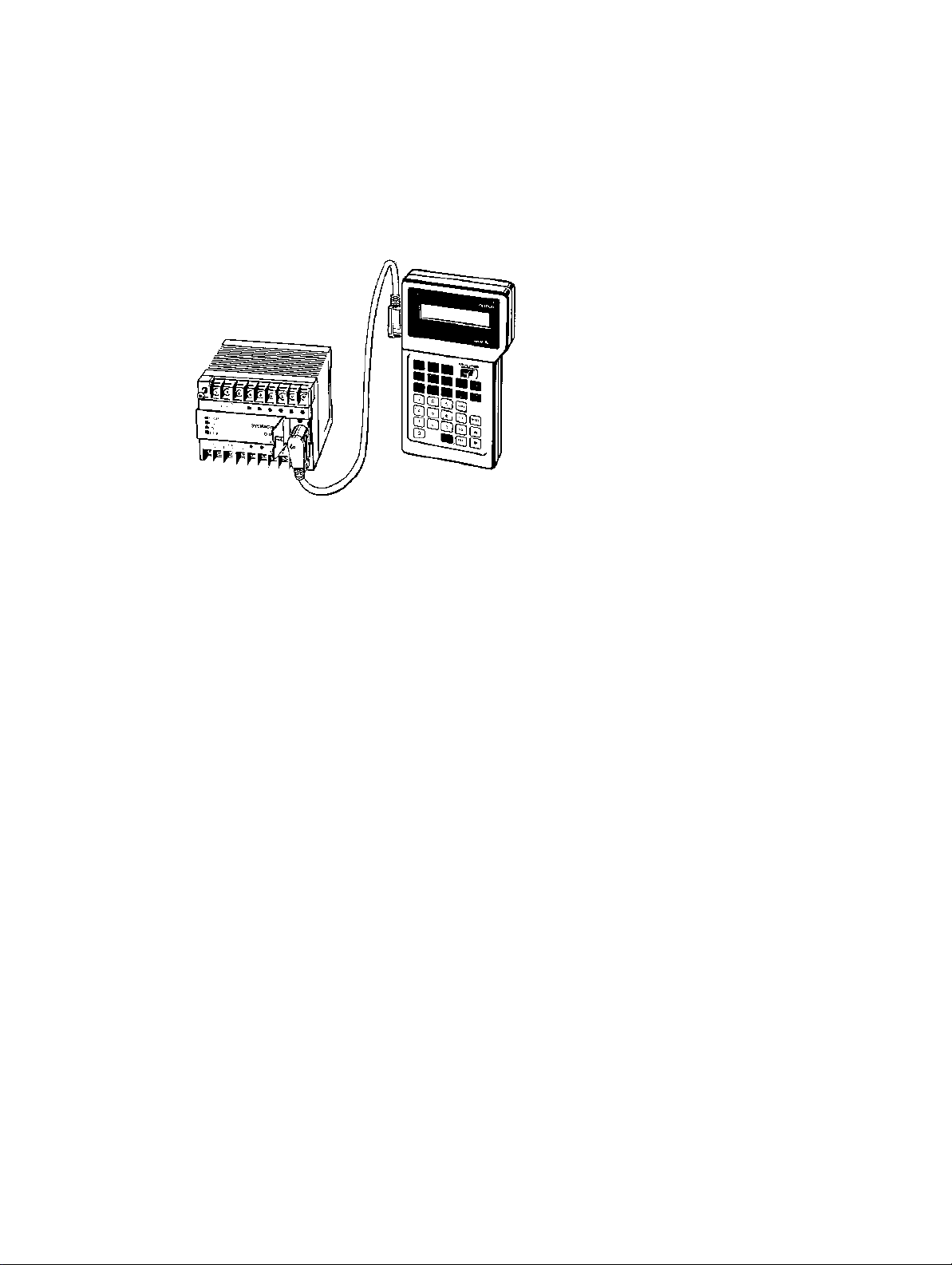
SP10
Power supply Inputs
Power terminals
for external supply
24 VDC, 0.1 A (see note 1)
OutputsNC
Analog timer
setting adjustment
Programming Console/
Link Adapter connector
5
Page 16
Units Section 1-3
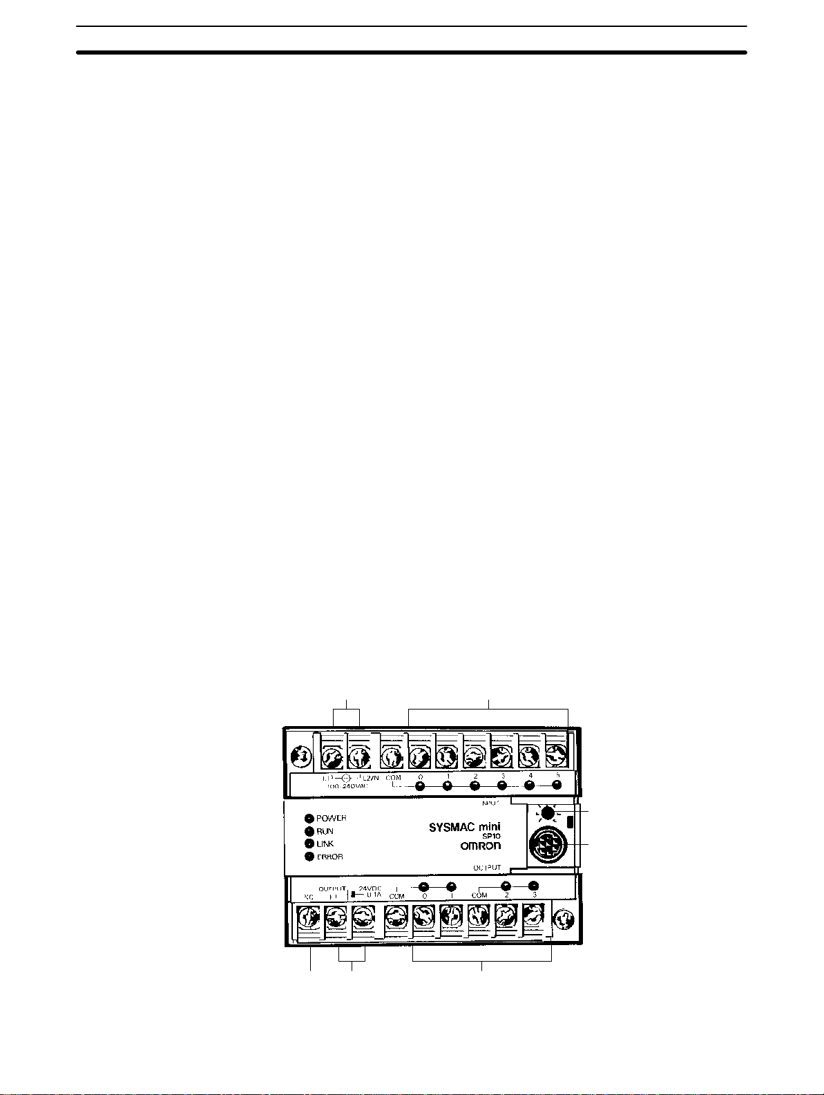
SP16 and SP20 The SP20 is essentially the same as the SP16. The SP16 is shown below.
Power supply
Power terminals
for external supply
24 VDC, 0.2 A (see note 1)
RDM(23) input
(See note 3)
Note 1. The power terminals for external supply are provided for the 100 to 240
Inputs
Analog timer 1
setting adjustment
Programming Console/
Link Adapter connector
Analog timer 2
setting adjustment
Outputs NC
VAC model (SP__-__-A) only.
2. Connect nothing to the NC terminal.
3. Input 000 is the counter input and 001 is the hard reset input for the RE-
VERSIBLE DRUM COUNTER, RDM(23). When RDM(23) isn’t being
used, these terminals can be used as normal input points but the input
signal must be below 1 kHz.
Indicators The PC has four indicators on the front panel, POWER, RUN, LINK, and ER-
ROR. The functions of the indicators are presented as follows.
POWER (green): Lit while power is supplied.
RUN (green): Lit when the PC is in RUN mode and operating normally.
LINK(green): Lit when the PC Link is operating normally.
ERROR(red): Lights when self-diagnosis detects an error. The PC will
stop operating.
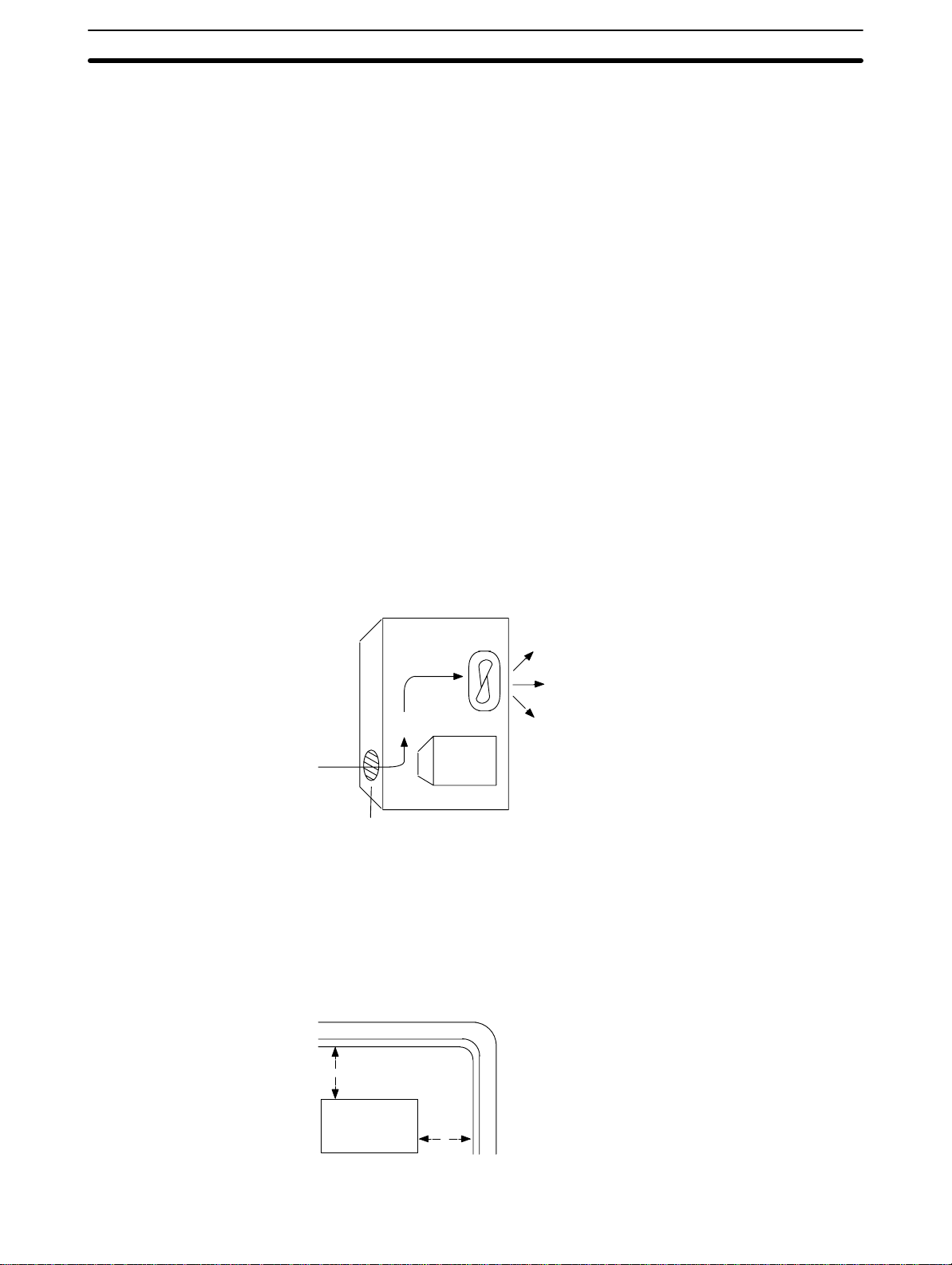
1-3-2 Programming Console
The Programming Console is shown below.
Display
Memory card access indicator
Connecting
cable connector
Mode switch
Key pad
Memory card slot
6
Page 17
Units Section 1-3
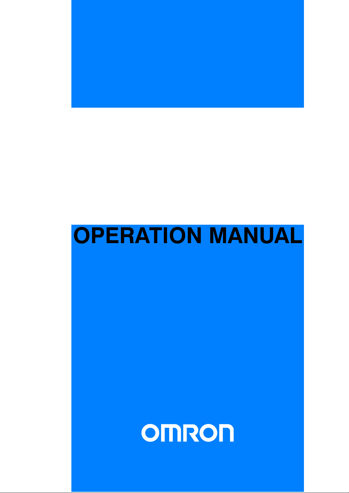
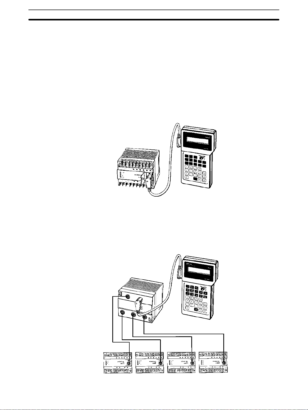
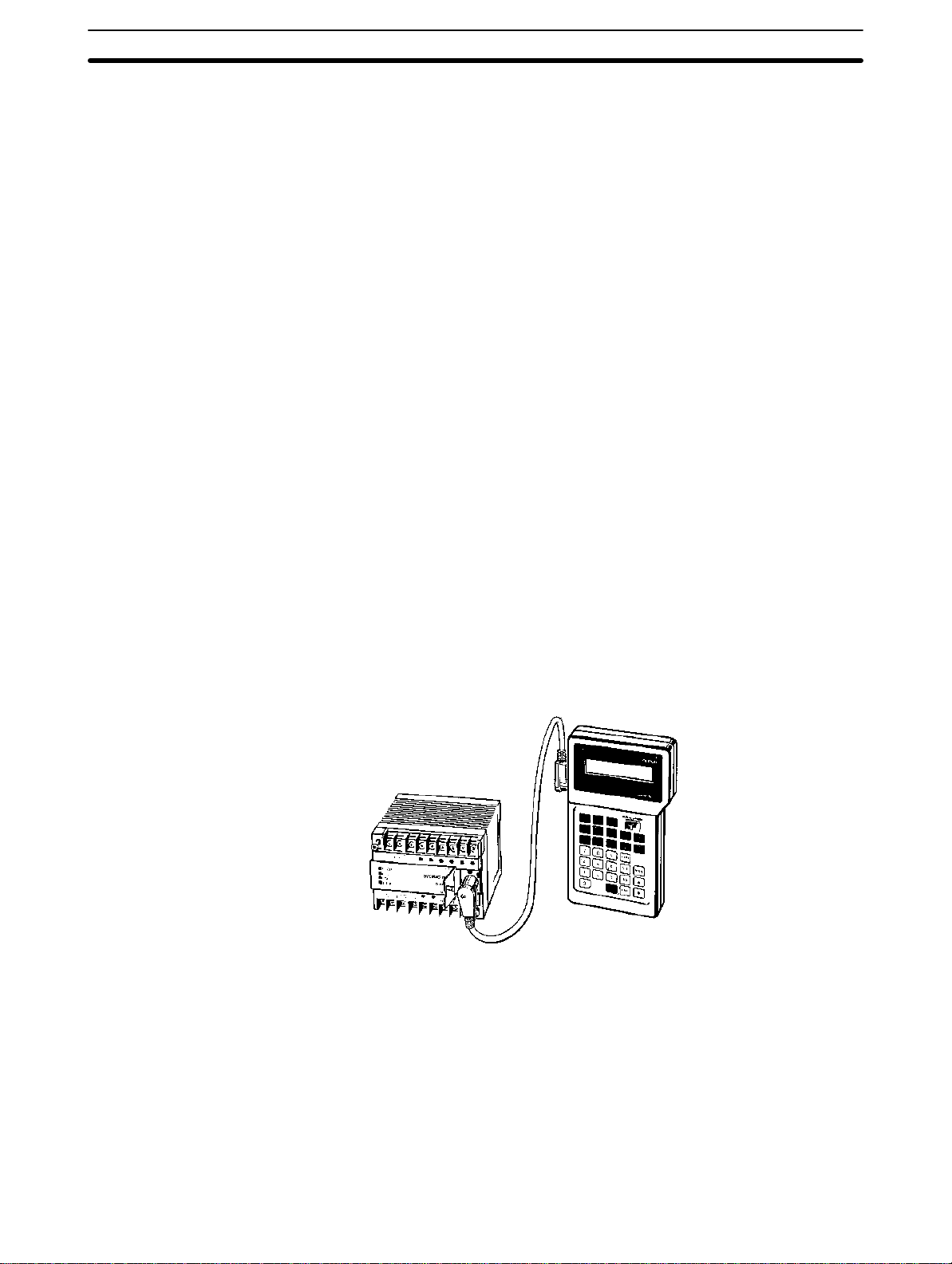
The Programming Console is used to write and transfer programs to the PC.
It is also used to monitor operation and modify data. The Programming Console can be connected directly to the PC for single PCs. It can also be connected via a Link Adapter when PCs are connected in a PC Link configuration to access each PC individually without reconnection.
Note PCs connected to a Link Adapter cannot be directly connected to a Program-
ming Console. The Programming Console is connected to the Link Adapter.
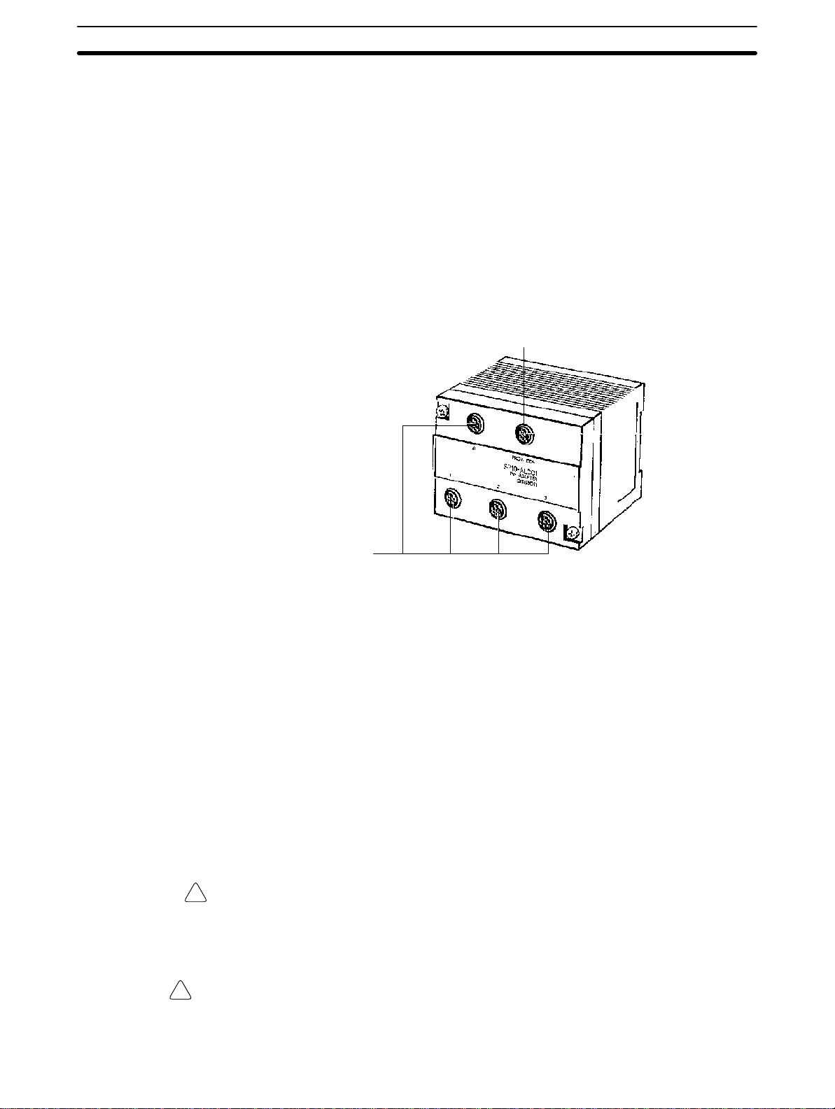
1-3-3 Link Adapter
The Link Adapter is shown below. The Link Adapter is used to link up to four
CPUs so that data can be transferred between the CPUs and so that all of
the CPUs can be accessed from the Programming Console from a single
connection point. For details refer to
1-4 PC Configuration
Programming Console
Connecting Cable Connector
.
CPU Connecting
Cable Connectors
1-3-4 Memory Cards
The Programming Console provides the ability to backup programs. The
Memory Card slot located at the base of the keyboard allows programs to be
transferred directly to and from the Programming Console. Each Card has a
built-in battery to preserve data.
Only one model of Memory Card, HMC-ES141, may be used. Each Memory
Card has 16 Kbytes of S-RAM. One Memory Card can hold up to 26 SP10
programs or up to 18 SP16 or SP20 programs.
A battery is built-in to the Memory Card to allow the data to be retained. The
battery must be replaced within five years to ensure data is not lost. To remove the battery, insert a sharp object, like a pen tip, into the hole at the bottom right of the card. The new battery must be inserted within one minute of
removing the old one.
Memory Cards have a write-protect switch. When the switch is ON, writing
operations to the memory card will not be possible.
Caution While the Memory Card is being accessed, the M/C ON LED on the Program-
!
ming Console will be lit. If the Memory Card is removed out from the Programming Console while the LED is ON, the data contained in memory on the Card
may be damaged.
WARNING Do not short the positive and negative terminals, charge, take apart, or throw
!
into fire a Memory Card. The battery inside the card may explode, burst into fire,
or leak, causing a potentially dangerous or even fatal accident.
7
Page 18
PC Configuration Section 1-4
1-4 PC Configuration
The SP-series PCs can be configured to control a control system of from 10
through 80 I/O points. An SP10 provides 10 I/O points (6 input and 4 output
points), an SP16 provides 16 I/O points (10 input and 6 output points), and
an SP20 provides 20 I/O points (12 input and 8 output points). A maximum of
4 SP-series PCs can be linked together via a Link Adapter, making a maximum of 80 I/O points with 4 SP20s.
1-4-1 Basic Configuration
When only one SP-series PC is used, the number of I/O points available is
10 with the SP10, 16 with the SP16, or 20 with the SP20. Here, the Programming Console is connected directly to the CPU for programming and operation.
Connecting Cable
SP10-CN__1
PC
SP10-PRO01-V1
1-4-2 Expanded System Configuration: PC Links
Up to four PCs can be linked with a Link Adapter to increase the number of
I/O points to 80 maximum. Although each PC still operates on its own program, no special programming is needed to transfer data between the PCs
via LR bits. Up to 128 bits of data (32 bits per PC) can be shared between
the PCs through their LR areas. Refer to
SP10-AL001
Link Adaptor
3-2-5 LR Area
for details on LR bits.
SP10-PRO01-V1
Programming
Console
SP10-CN__1 Connecting Cables
SP__ #0 SP__ #1 SP__ #2 SP__ #3
8
Page 19

PC Configuration Section 1-4
Note 1. When two or more PCs are linked, apply power to all of the PCs at once
or to PC #0 last.
2. When using a Link Adapter, one PC must be connected to connector
number 0 on the Link Adapter.
3. Once CPUs are connected to the Link Adapter and turned ON, unit num-
bers are automatically assigned to the CPUs by the Link Adapter. Do not
change the point of connection of any CPU after a unit number has been
assigned to it. If CPUs are connected to a connecter for a different unit
number, unpredictable errors will occur during operation.
Unit Numbers When four PCs are linked, each are given a number from 0 through 3 de-
pending on which connector on the Link Adapter is used. PC #0 controls LR
data transfers between the PCs. The Programming Console is connected to
the Link Adapter and can program and monitor any of the four PCs.
9
Page 20

SECTION 2
Installation
This section provides information on mounting and wiring the CPUs and on I/O specifications. Basic unit connections
are described in 1-4 PC Configuration. Detailed specifications are provided in Appendix B Specifications.
2-1 Dimensions 12 . . . . . . . . . . . . . . . . . . . . . . . . . . . . . . . . . . . . . . . . . . . . . . . . . . . . . . .
2-2 Installation 13 . . . . . . . . . . . . . . . . . . . . . . . . . . . . . . . . . . . . . . . . . . . . . . . . . . . . . . .
2-2-1 Installation Environment 13 . . . . . . . . . . . . . . . . . . . . . . . . . . . . . . . . . . . .
2-2-2 Cooling 14 . . . . . . . . . . . . . . . . . . . . . . . . . . . . . . . . . . . . . . . . . . . . . . . . .
2-2-3 Preventing Noise 14 . . . . . . . . . . . . . . . . . . . . . . . . . . . . . . . . . . . . . . . . . .
2-2-4 Mounting Requirements 15 . . . . . . . . . . . . . . . . . . . . . . . . . . . . . . . . . . . .
2-3 Wiring 15 . . . . . . . . . . . . . . . . . . . . . . . . . . . . . . . . . . . . . . . . . . . . . . . . . . . . . . . . . . .
2-3-1 Power Supply 15 . . . . . . . . . . . . . . . . . . . . . . . . . . . . . . . . . . . . . . . . . . . .
2-3-2 I/O Connections 16 . . . . . . . . . . . . . . . . . . . . . . . . . . . . . . . . . . . . . . . . . . .
2-3-3 Precautions 20 . . . . . . . . . . . . . . . . . . . . . . . . . . . . . . . . . . . . . . . . . . . . . .
2-4 Programming Console 20 . . . . . . . . . . . . . . . . . . . . . . . . . . . . . . . . . . . . . . . . . . . . . .
2-4-1 Designating the PC 21 . . . . . . . . . . . . . . . . . . . . . . . . . . . . . . . . . . . . . . . .
2-4-2 Input Filters 22 . . . . . . . . . . . . . . . . . . . . . . . . . . . . . . . . . . . . . . . . . . . . . .
11
Page 21
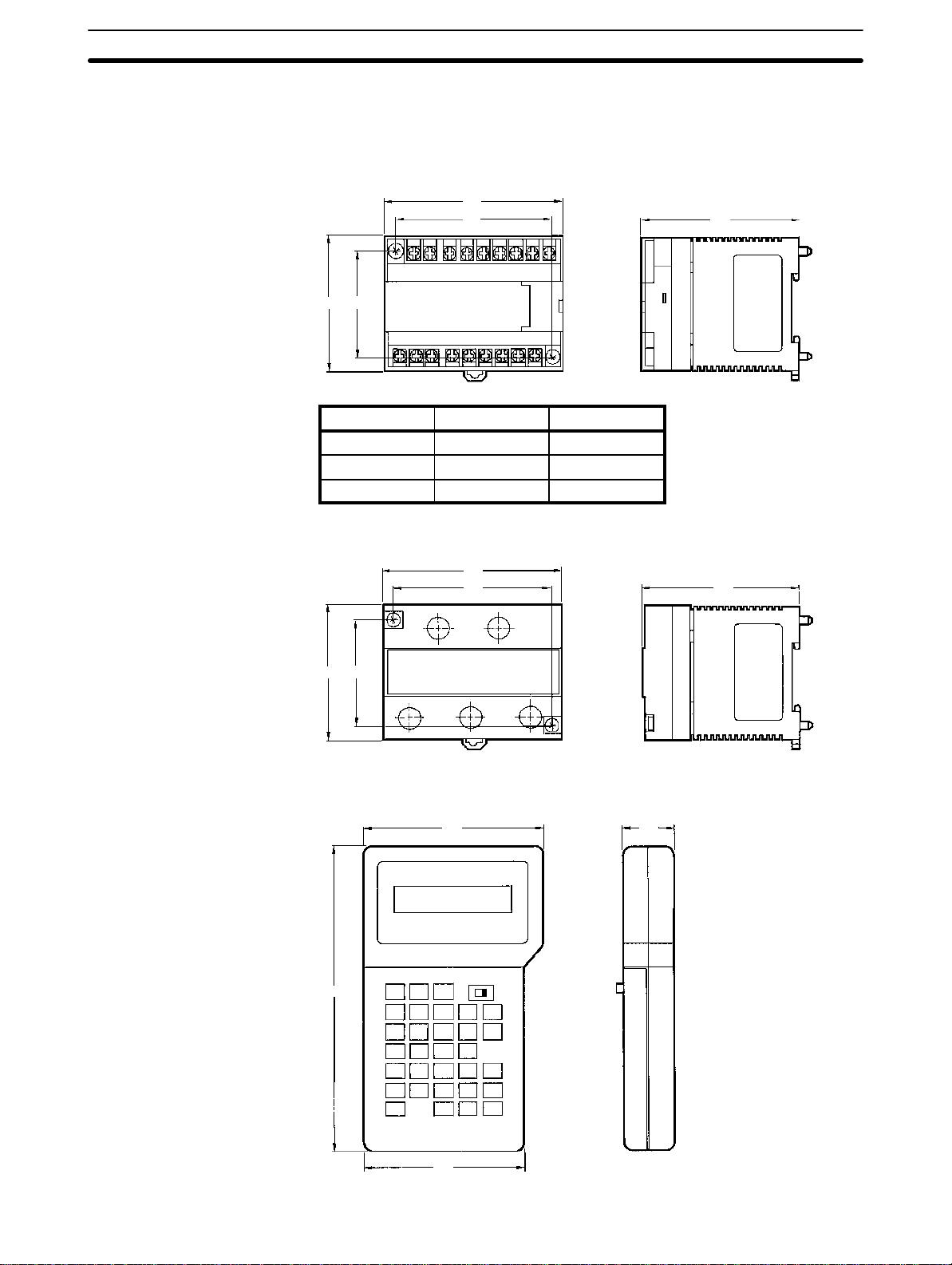
Dimensions Section 2-1
2-1 Dimensions
This section gives mounting dimensions. All dimensions are in millimeters.
CPUs
Link Adapter
SP10-D_-_, SP16-D_-_, SP20-D_-_
A
B
68 53
PC model Dimension A Dimension B
SP10-D_-_ 92 81
SP16-D_-_ 135 124
SP20-D_-_ 160 149
SP10-AL001
92
81
81
81
Programming Console
68 53
SP10-PRO01-V1
155
91
25
12
81
Page 22
Installation Section 2-2
Surface Mounting Dimensions
2-M4
53
A
PC model Dimension A
SP10-D_-_ 81
SP16-D_-_ 124
SP20-D_-_ 149
Mounting Track
The SP-series PCs can be mounted onto DIN Tracks.
Model No. Length (L)
PFP-50N 50 cm
PFP-100N 1 m
PFP-100N2 1 m
PFP-50N/PFP-100N
4.5
25 25
15
10
PFP-100N2
4.5
25 25
15
10
1000 (500) *
1000
End Plate (PFP-M)
M4x8
50
11.5
10
7.3±0.15
35±0.3 27±0.5
35±0.3
27 24
10
6.2
1.8
1
35.5
1.8
1.3
4.8
1
16
29.2
35.3
2-2 Installation
2-2-1 Installation Environment
Although the SP-series Programmable Controllers are highly reliable and
durable, a number of factors should be considered when installing them. Do
not expose an SP-series PC to the following conditions.
13
Page 23
Installation Section 2-2
• An ambient temperature that falls below 0° or exceeds 55°C for the CPU, or
that falls below 0°or exceeds 45°C for the Programming Console.
• Abrupt changes in temperature that cause condensation.
• A relative humidity less than 10% or greater than 90%.
• Corrosive or flammable gas.
• Dust, salt, or iron particles.
• Direct vibration or shock.
• Direct sunlight.
• Splashes of water, oil, or chemicals.
2-2-2 Cooling
There are two points to consider in order to ensure that the PC does not
overheat. The first is the clearance between the CPUs and control panel surround them, and the second is the installation of a cooling fan.
Clearance The CPUs need to have sufficient room between them to allow for I/O wiring,
and additional room to ensure that the wiring does not hamper cooling. The
CPU’s must be mounted close enough so that the length of the Connecting
Cable between any CPU and the Link Adapter does not exceed 4 meters.
Cooling Fan Ensure adequate ventilation is provided for the PCs. A cooling fan is not al-
ways necessary, but may be needed if the PC is mounted in a warm or enclosed area or over a source of heat. Although it is best to avoid installing the
PC in a warm area, use a cooling fan or an air conditioner, as shown in the
following illustration, to maintain the ambient temperature within specifications.
2-2-3 Preventing Noise
In order to prevent noise from interfering with the operation of the PC, use
AWG 14 twisted-pair cables (cross-sectional area of at least 2 mm
mount the PC in a control panel in which high-power equipment is installed
and make sure the point of installation is at least 200 mm away from power
cables, as shown in the following diagram. Ground the panel to which the PC
is mounted.
Control Panel
Louver
Power lines
200 mm min.
PC
Fan
2
). Do not
14
PC
200 mm min.
Page 24
Wiring Section 2-3
Whenever possible, use wiring conduit to hold the I/O wiring. Standard wiring
conduit should be used, and it should be long enough to completely contain
the I/O wiring and keep it separated from other cables.
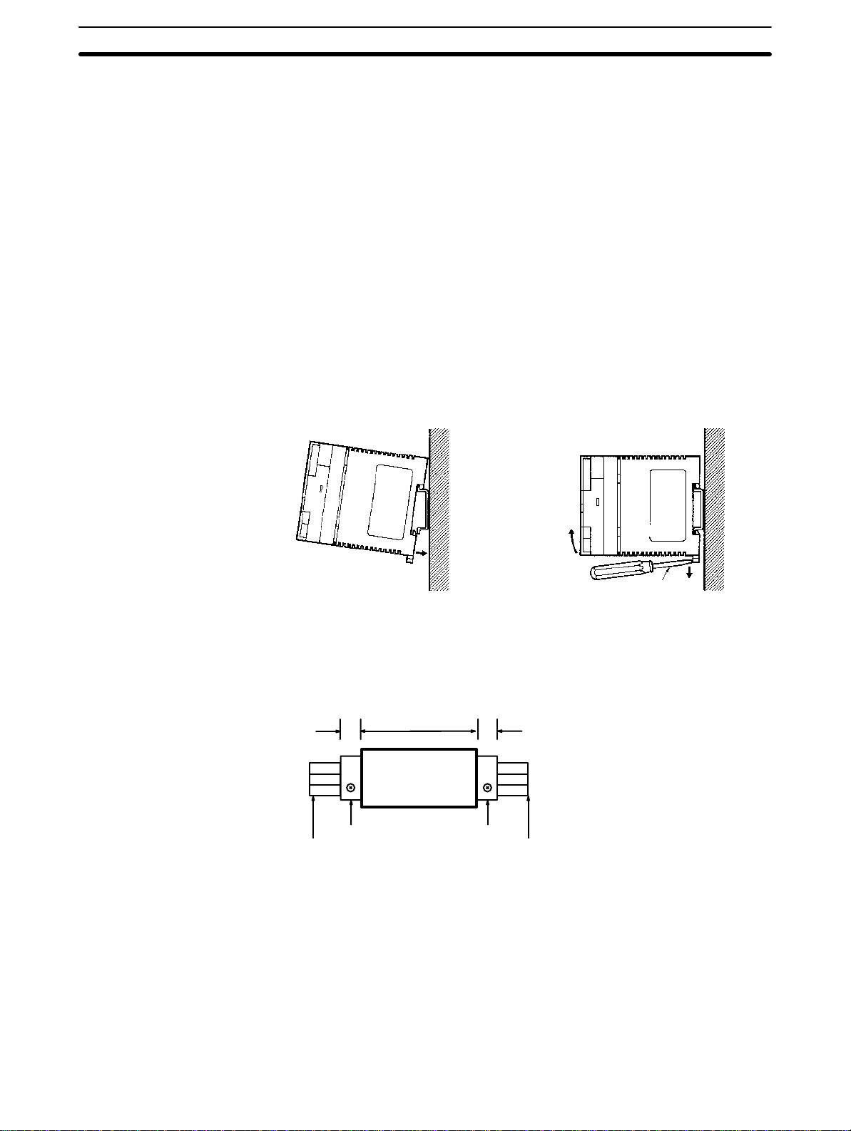
2-2-4 Mounting Requirements
The system consists of from one to four CPUs and, if more than one CPU is
used, a Link Adapter. The Units may be mounted horizontally or vertically, as
desired. Do not mount a Unit on its side. The Unit should be mounted with
the printing on the front panel oriented as it would normally be read. The PC
can be mounted using DIN Track or mounted directly to any sturdy support
meeting the environmental specifications listed in
Track Mounting The PC may be mounted using DIN Track if desired. Use DIN Track 35 mm
wide. There is a groove on the back of the Unit that is used to attach it to the
DIN Track. When mounting to DIN Track, be sure to remove the mounting
screws.
Appendix B Specifications.
RemovalMounting
Note Remove the mounting screws when mounting on a track.
2-3 Wiring
Note Do not wire the terminal marked “NC.”
2-3-1 Power Supply
Screwdriver
Engage the top hook to the
track and push the PC in until
the bottom hook locks onto the
track.
Push down the bottom hook
with a screwdriver and push
the PC upward.
Attach an End Plate to the left and right sides of the Unit to hold it in place.
1010
SP-series PC
PFP-M End Plate
DIN Track DIN Track
PFP-M End Plate
DIN Track
PFP-100N (1 m)
PFP-50N (0.5m)
PFP-100N2 (1 m)
Use independent power sources for the inputs, the output loads, and the PC.
Voltage fluctuations caused by current surges to motors may affect operation
of the PC. When using more than one PC, use a separate power supply for
15
Page 25
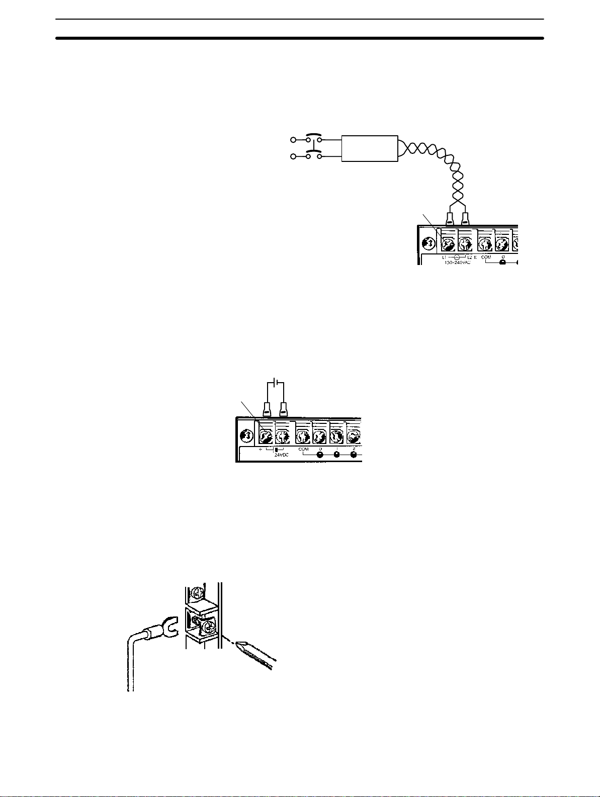
Wiring Section 2-3
each PC, firstly to prevent voltage drops caused by surge currents and secondly, to prevent the breaker from malfunctioning.
The following diagrams show the proper way to connect the power source to
the PC. Refer to
AC Connections
Appendix B Specifications
for detailed specifications.
AC Power Source
• Supply 100 to 240
VAC, 50/60 Hz
Breaker
Power Line
1:1 Isolation
Transformer
M3.5 screws
• Use twisted pair cable
(cross-sectional area of
2
2 mm
min.)
To reduce noise interference from the power lines, use twisted pair cables.
Noise can also be significantly reduced by connecting a 1-to-1 isolation
transformer.
Note Do not short the positive and negative lines.
DC Connections Supply 24 VDC and keep voltage fluctuations within the specified range.
+
M3.5 screws
2-3-2 I/O Connections
Connect the I/O devices to the I/O terminals using wire with a cross-sectional
area of 1.04 to 2.63 mm
self-rising pressure plates. Connect the lead wires to the terminals as shown
below. Tighten the screws with a torque of 8 kg-cm maximum.
If you wish to attach solderless type terminals to the ends of the lead wires,
use terminals having the following dimensions.
16
2
. The terminals have screws with M3.5 heads and
Page 26
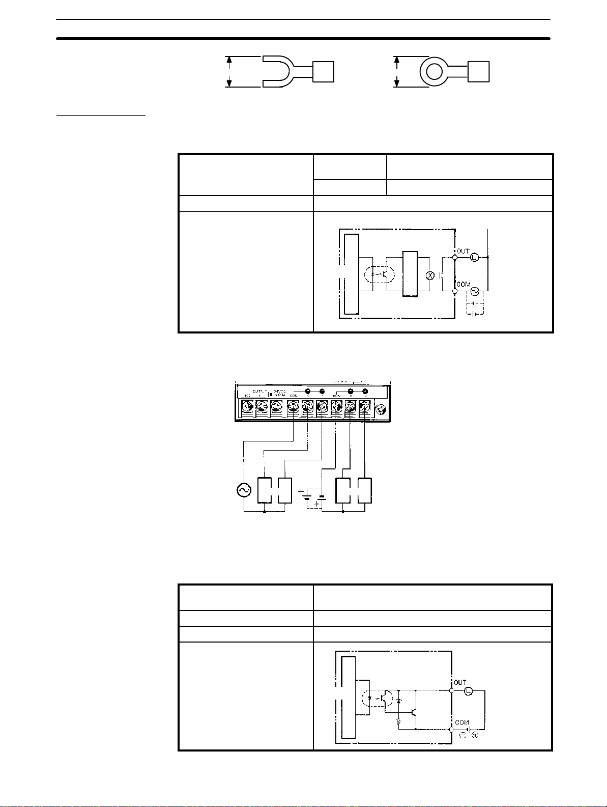
Wiring Section 2-3
7.5 mm max.7.5 mm max.
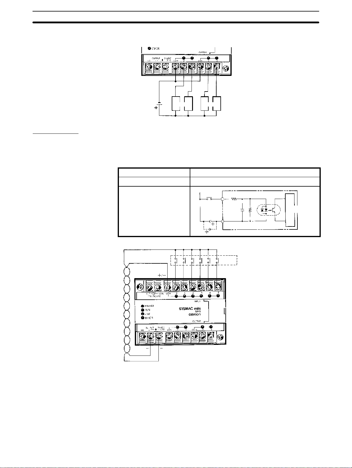
Output Circuits
Refer to
Relay Contact Outputs
Maximum switching
capacity
Minimum switching capacity 5 VDC, 100 mA
Circuit configuration
Appendix B Specifications
Resistive loads 250 VAC, 2 A (cosf=1), 24 VDC, 2A/pt
Inductive loads 250 VAC, 0.5 A (cosf=0.4)/pt
for detailed specifications.
Insulating
Photocoupler
Internal
circuit
Relay’s power (24 V)
is internally supplied
The following example uses an SP10 CPU.
250 VAC
max.
Loads
AC load
power supply
24 VDC
Loads
DC load
power supply
Internal
circuit
Use seperate
power supplies
for load power
sources
250 VAC,
24 VDC max.
Transistor Outputs
Maximum switching
24 VDC
+10%
capacity
Leakage current 0.1 mA max.
Residual voltage 1 V max.
Circuit configuration
Internal
circuit
/
–15%
Insulating
photocoupler
, 0.3 A
24 VDC
17
Page 27
Wiring Section 2-3
The following example uses an SP10 CPU.
Input Circuits
Load power
supply 24 VDC
Loads Loads
Either positive or negative poles of the power supply can be connected to the
common (COM) terminals, enabling connection of both PNP (negative common) and NPN (positive common) inputs.
24 VDC
+10%
COM
/
–15%
3.3 kΩ 470 ΩIN
1,000 pF
Insulating
photocoupler
Input devices
Internal
circuit
Input voltage 24 VDC
Input current 7 mA Typ. (24 VDC)
Circuit configuration
18
The power source of the SP10 for external supply is rated at 0.1 A, 24 VDC
max., and the power source of the SP16 and SP20 is rated at 0.2 A, 24 VDC
max. The input circuit consumes about 7 mA (typ. at 24 VDC) per input point.
Transistor outputs with a current consumption up to 0.2 A can be used with
the SP10, and a current consumption up to 0.32 A with the SP16 and SP20.
Relay contact outputs require a current of 0.013 A each, so when all of the
relays are ON, the external power supply capacity is 0.1 A for the SP10 and
0.2 A for the SP16 and SP20. When using the SP10 as the power source for
Page 28
Wiring Section 2-3
input devices such as sensors, etc., make sure that the power consumption
of the devices does not exceed the ratings of the PC.
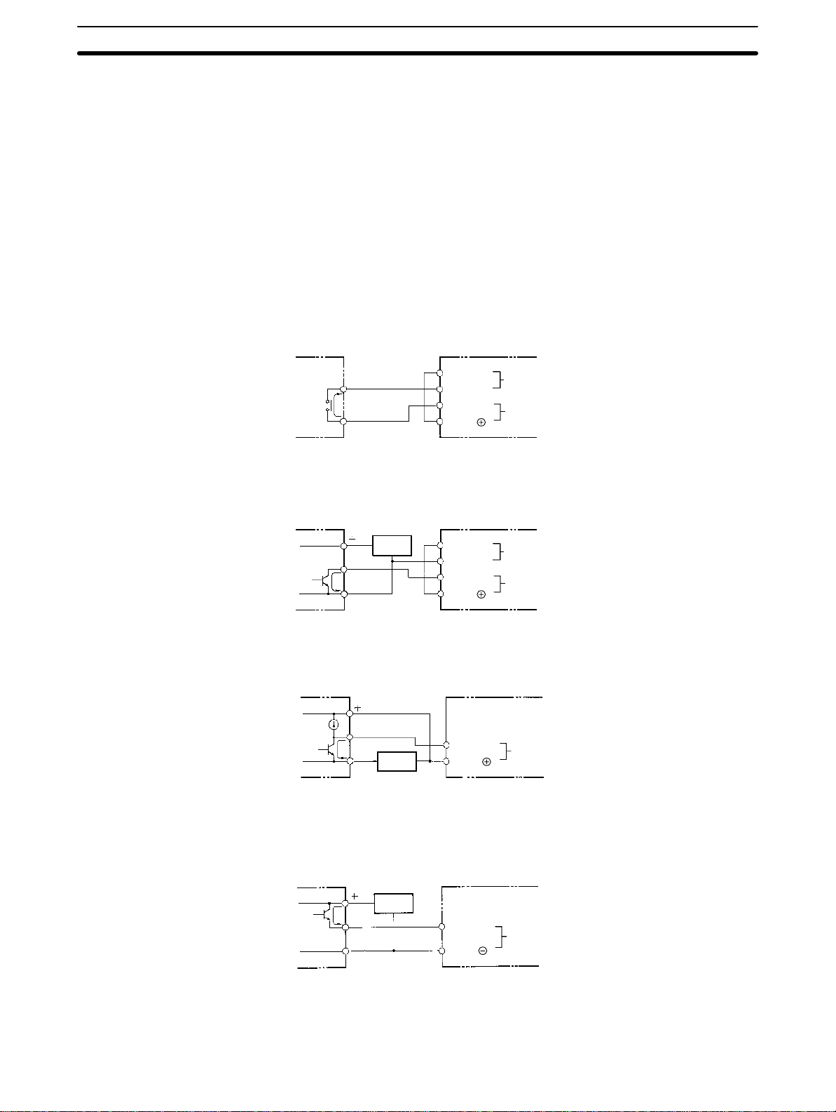
DC Input Examples The following diagrams show the correct way to wire the terminals on the
CPU. When wiring, work carefully to ensure that all terminals are wired correctly. If an input device is connected to an output point, damage may result.
Appen-
DC Input Devices
Check all I/O devices to ensure they meet the specifications (refer to
Specifications).
dix B
The DC inputs in the following diagrams are NPN (positive common). Reverse the polarity if PNP (negative common) is used.
Use the CPU’s 24 VDC power supply output to supply power to inputs. If the
maximum output current of 0.3 A is not sufficient, use a separate DC power
supply.
NPN Open-collector Outputs
NPN Current Outputs
Current
regulator
7 mA
Output
7 mA
0 V
Output
7 mA
0 V
Sensor
power
supply
Sensor
power
supply
24 VDC
0 V
IN
COM
24 VDC
0 V
IN
COM
Use the same power supply
for the input and sensor.
IN
COM
Power source for
external supply
DC input
Power source for
external supply
DC input
DC input
SP__
SP__
SP__
PNP Current Outputs
Sensor
power
supply
Output
7 mA
0 V
IN
COM
DC input
SP__
Note When using the DC model (SP__-D_-D), do not input the signal through a NC
contact (which makes the PC operate when the externally input signal turns
19
Page 29
Programming Console Section 2-4
OFF). Proper operation for power interruptions will not be possible if NC contacts are used in conjunction with counter, shift, or keeping (latching) instructions.
2-3-3 Precautions
Unit Sticker A sticker is provided on the upper face of the CPU to prevent foreign objects,
such as wire clippings, from entering the CPU. Leave this protective sticker
on until the CPU is ready for operation. The sticker must be removed before
operation to enable proper cooling.
Contact Outputs High inductance on for contact outputs will reduce relay life. Keep inductance
low and use an arc suppressor (such as a diode for DC loads). This is particular important with inductive DC loads.
Vibration Relay operation may be adversely affected if the relay is located near contac-
tors, valves, motors, or other devices that produce vibration.
Protective Circuits We recommend the use of arc suppressors to increase contact life and allevi-
ate the affects of noise. Arc suppressors, however, will delay release time
somewhat and, if used incorrectly, they can inhibit proper operation. The
most common arc suppressors for AC are capacitor-resistor circuits and varistor circuits; for DC: capacitor-resistor circuits, diode circuits, and varistor
circuit. Do not use a capacitor without a resistor as the charging current flow
to the capacitor when current is turned ON can cause the contacts to fuse.
2-4 Programming Console
Open the connector cover of the PC, align the notch on the connector, and
press the connector into place.
Connection to a CPU
Connecting Cable
SP10-CN__1
PC
SP__
SP10-PRO01-V1
20
Page 30
Programming Console Section 2-4
Connection to a Link Adaptor
SP10-AL001
Link Adaptor
SP10-PRO01-V1
Programming
Console
SP10-CN__1 Connecting Cables
SP__ #0 SP__ #1 SP__ #2 SP__ #3
Connecting Cable Use one of the following Connecting Cables to connect the Programming Console.
SP10-CN221 (2 m)
SP10-CN421 (4 m)
Note The sum of the cable lengths between Unit #0 and the Link Adapter and be-
tween the Link Adapter and the Programming Console must be 4.2 m maximum.
2-4-1 Designating the PC
Any of the PCs connected in a PC Link may be accessed through the Link
Adapter using the Programming Console. Use the following key sequence to
specify the number of the desired PC. The PC can be designated in either
PROGRAM or RUN mode.
AB
0 PC 0-3? PC ?
A
The PC’s operation or operation mode is not affected by changing the PC
designation. When the mode switch of the Programming Console and the
21
Page 31

Programming Console Section 2-4
operation mode of the PC being monitored are identical, the following message is displayed. The number in the top left corner indicates the number of
the PC being monitored, in this case PC #1.
1-000
B
When the mode switch of the Programming Console and the operation mode
of the PC being monitored are not identical, the following message is displayed.
<RUN>
B
MODE SET ERR
In this example, the message indicates that the Programming Console is set
to PRGM (program) mode, and that PC #1 is set to RUN mode. To clear the
error and reset the corresponding alarm, turn the Programming Console
mode to RUN and then change it back to PRGM mode. PC #1 will change to
PRGM mode.
Note If there is a communication error, the display will read “COMM ERR”.
2-4-2 Input Filters
External input
Input detection time
To prevent the PC from malfunctioning due to the chattering (bouncing) of the
input device signals or induced noise, the input signals are received via a
filter. The filter may be adjusted so that input pulses of a duration less than a
minimum specified duration of the filter are ignored. The minimum duration
before the detection of an input signal may be set to 0, 1, 5, or 10 ms. The
following diagram illustrates the use of a filter.
tt
The input detection time, t, for the various possible settings is given in the
following table. The “key” column shows which key is pressed to input each
setting in the key sequence below.
Key Setting Actual detection time
0 0 ms t = 150 µs
1 1 ms t = 1 to 1.5 ms
2 5 ms t = 5 to 5.5 ms
3 10 ms t = 10 to 10.5 ms
Filter Value Settings
22
During the period t to t + 0.5 ms, the positive and negative transitions of the
input signal may or may not be detected.
The filter values are set using the Programming Console. The input circuits
are grouped into three groups. The circuits included in each group depend on
Page 32

Programming Console Section 2-4
the PC, as shown in the table below. A different filter value can be set for
each group. The filter values can be set in PROGRAM mode only and must
be set before operating the PC. The filter values are set simultaneously in the
PC and in the Programming Console.
PC model Group 1 inputs Group 2 inputs Group 3 inputs
SP10-D_-_ 0 to 2 3 to 5 None
SP16-D_-_ 0 and 1 2 to 5 6 to 9
SP20-D_-_ 0 and 1 2 to 9 10 and 11
Always set the filter values after transferring the program and before starting
operation. Set the filter value to 5 or 10 ms when the PC is installed in environments subject to noise, or when input devices that may cause chattering
are connected to the PC. If the filter value is set to 0 or 1 ms, be sure that the
input wiring is carefully installed to prevent interference.
Key Sequence
Input 0 to specify 0 ms, 1 for 1 ms, 2 for 5 ms, and 3 for 10 ms.
Group 1 Group 2
Group 3
ABC
The following diagrams illustrate the Programming Console displays at the
respective positions marked in the key sequence diagram.
0 FILTER VAL SETGROUP1 SE
A
T NO.?
0 FILTER VAL SET
B
GROUP2 SET NO.?
0 FILTER VAL SET
C
GROUP3 SET NO.?
D
Key Sequence
0 FILTER VAL OK
D
Set the filter values of groups 1, 2, and 3 at the same time. After entering the
filter values, read them on the Programming Console for confirmation. Use
the following key sequence. Reading is possible in either RUN or PROGRAM
mode.
The Programming Consoles will display the information in the following formats.
23
Page 33

Programming Console Section 2-4
SP10-PRO01
0 FILTER VAL GROUP 1-1 2-2
Group 2: 5 ms
Group 1: 1 ms
SP10-PRO01-V1
The display will show the settings for groups 1 and 2 when the Programming
Console is connected to an SP10.
0 PC :0-1
ProCo:0-2
0 PC :0-1-2
ProCo:0-2-2
Note If a pulse width of less than 150 µs is input, the SP-series CPU and the Pro-
PC settings
Group 1: 0 ms; group 2: 1 ms.
Programming Console settings
Group 1: 0 ms; group 2: 5 ms.
The display will show the settings for groups 1, 2, and 3 when the Programming Console is connected to an SP16 or SP20.
PC settings
Group 1: 0 ms; group 2: 1 ms; group 3: 5 ms.
Programming Console settings
Group 1: 0 ms; group 2: 5 ms; group 3: 5 ms.
gramming Console will not work properly.
24
Page 34

SECTION 3
Programming
This section takes you all the way through the programming procedure from understanding memory area allocation to
debugging and executing the program. Section 4 Operation will then provide procedures for monitoring PC operation
and manipulating data after you have written, input, and debugged the program.
3-1 Introduction 27 . . . . . . . . . . . . . . . . . . . . . . . . . . . . . . . . . . . . . . . . . . . . . . . . . . . . . .
3-2 Memory Areas 27 . . . . . . . . . . . . . . . . . . . . . . . . . . . . . . . . . . . . . . . . . . . . . . . . . . . .
3-2-1 Data Area Structure 28 . . . . . . . . . . . . . . . . . . . . . . . . . . . . . . . . . . . . . . . .
3-2-2 I/O Bits 30 . . . . . . . . . . . . . . . . . . . . . . . . . . . . . . . . . . . . . . . . . . . . . . . . .
3-2-3 Work Bits 31 . . . . . . . . . . . . . . . . . . . . . . . . . . . . . . . . . . . . . . . . . . . . . . . .
3-2-4 Dedicated Bits 31 . . . . . . . . . . . . . . . . . . . . . . . . . . . . . . . . . . . . . . . . . . . .
3-2-5 LR Area 33 . . . . . . . . . . . . . . . . . . . . . . . . . . . . . . . . . . . . . . . . . . . . . . . . .
3-2-6 DR Area 36 . . . . . . . . . . . . . . . . . . . . . . . . . . . . . . . . . . . . . . . . . . . . . . . . .
3-2-7 TC (Timer/Counter) Area 36 . . . . . . . . . . . . . . . . . . . . . . . . . . . . . . . . . . .
3-3 The Programming Console 37 . . . . . . . . . . . . . . . . . . . . . . . . . . . . . . . . . . . . . . . . . . .
3-3-1 The Keyboard 38 . . . . . . . . . . . . . . . . . . . . . . . . . . . . . . . . . . . . . . . . . . . .
3-3-2 PC Modes 39 . . . . . . . . . . . . . . . . . . . . . . . . . . . . . . . . . . . . . . . . . . . . . . .
3-4 Basic Programming 39 . . . . . . . . . . . . . . . . . . . . . . . . . . . . . . . . . . . . . . . . . . . . . . . .
3-4-1 Terminology 39 . . . . . . . . . . . . . . . . . . . . . . . . . . . . . . . . . . . . . . . . . . . . .
3-4-2 Mnemonic Code 41 . . . . . . . . . . . . . . . . . . . . . . . . . . . . . . . . . . . . . . . . . .
3-4-3 Ladder Instructions 42 . . . . . . . . . . . . . . . . . . . . . . . . . . . . . . . . . . . . . . . .
3-4-4 OUTPUT and OUTPUT NOT 44 . . . . . . . . . . . . . . . . . . . . . . . . . . . . . . .
3-4-5 The END Instruction 44 . . . . . . . . . . . . . . . . . . . . . . . . . . . . . . . . . . . . . . .
3-4-6 Logic Block Instructions 45 . . . . . . . . . . . . . . . . . . . . . . . . . . . . . . . . . . . .
3-4-7 Coding Multiple Right-hand Instructions 51 . . . . . . . . . . . . . . . . . . . . . . .
3-5 Inputting the Program 51 . . . . . . . . . . . . . . . . . . . . . . . . . . . . . . . . . . . . . . . . . . . . . . .
3-5-1 Initial Programming Console Operation 51 . . . . . . . . . . . . . . . . . . . . . . . .
3-5-2 Designating the PC 52 . . . . . . . . . . . . . . . . . . . . . . . . . . . . . . . . . . . . . . . .
3-5-3 Clearing Memory 53 . . . . . . . . . . . . . . . . . . . . . . . . . . . . . . . . . . . . . . . . .
3-5-4 Clearing Error Messages 54 . . . . . . . . . . . . . . . . . . . . . . . . . . . . . . . . . . . .
3-5-5 Setting and Reading from Program Memory Address 54 . . . . . . . . . . . . .
3-5-6 Entering or Editing Programs 55 . . . . . . . . . . . . . . . . . . . . . . . . . . . . . . . .
3-5-7 Checking the Program 57 . . . . . . . . . . . . . . . . . . . . . . . . . . . . . . . . . . . . . .
3-5-8 Program Transfer 58 . . . . . . . . . . . . . . . . . . . . . . . . . . . . . . . . . . . . . . . . . .
3-5-9 Program Searches 61 . . . . . . . . . . . . . . . . . . . . . . . . . . . . . . . . . . . . . . . . .
3-5-10 Inserting and Deleting Instructions 61 . . . . . . . . . . . . . . . . . . . . . . . . . . . .
3-6 Advanced Programming 64 . . . . . . . . . . . . . . . . . . . . . . . . . . . . . . . . . . . . . . . . . . . . .
3-6-1 Interlocks 64 . . . . . . . . . . . . . . . . . . . . . . . . . . . . . . . . . . . . . . . . . . . . . . . .
3-6-2 Controlling Bit Status 65 . . . . . . . . . . . . . . . . . . . . . . . . . . . . . . . . . . . . . .
3-6-3 DIFFERENTIATE UP and DIFFERENTIATE DOWN 66 . . . . . . . . . . . .
3-6-4 KEEP 66 . . . . . . . . . . . . . . . . . . . . . . . . . . . . . . . . . . . . . . . . . . . . . . . . . . .
3-6-5 Self-maintaining Bits (Seal) 67 . . . . . . . . . . . . . . . . . . . . . . . . . . . . . . . . .
3-6-6 Work Bits (Internal Relays) 67 . . . . . . . . . . . . . . . . . . . . . . . . . . . . . . . . . .
3-6-7 Programming Precautions 69 . . . . . . . . . . . . . . . . . . . . . . . . . . . . . . . . . . .
25
Page 35

3-7 Instruction Set 71 . . . . . . . . . . . . . . . . . . . . . . . . . . . . . . . . . . . . . . . . . . . . . . . . . . . . .
3-7-1 Notation 71 . . . . . . . . . . . . . . . . . . . . . . . . . . . . . . . . . . . . . . . . . . . . . . . . .
3-7-2 Instruction Format 71 . . . . . . . . . . . . . . . . . . . . . . . . . . . . . . . . . . . . . . . . .
3-7-3 Data Areas, Definer Values, and Flags 71 . . . . . . . . . . . . . . . . . . . . . . . . .
3-7-4 Coding Right-hand Instructions 72 . . . . . . . . . . . . . . . . . . . . . . . . . . . . . .
3-7-5 LOAD, LOAD NOT, AND, AND NOT, OR, and OR NOT 74 . . . . . . . .
3-7-6 AND LOAD and OR LOAD 75 . . . . . . . . . . . . . . . . . . . . . . . . . . . . . . . . .
3-7-7 OUTPUT and OUTPUT NOT - OUT and OUT NOT 75 . . . . . . . . . . . . .
3-7-8 DIFFERENTIATE UP and DIFFERENTIATE DOWN -
3-7-9 KEEP - KEEP(12) 78 . . . . . . . . . . . . . . . . . . . . . . . . . . . . . . . . . . . . . . . . .
3-7-10 INTERLOCK and INTERLOCK CLEAR - IL(02) and ILC(03) 79 . . . . .
3-7-11 END - END(01) 81 . . . . . . . . . . . . . . . . . . . . . . . . . . . . . . . . . . . . . . . . . .
3-7-12 NO OPERATION - NOP(00) 81 . . . . . . . . . . . . . . . . . . . . . . . . . . . . . . . .
3-7-13 Timers and Counters 81 . . . . . . . . . . . . . . . . . . . . . . . . . . . . . . . . . . . . . . .
3-7-14 TIMER - TIM 83 . . . . . . . . . . . . . . . . . . . . . . . . . . . . . . . . . . . . . . . . . . . .
3-7-15 TIMER - TIMM(20) 86 . . . . . . . . . . . . . . . . . . . . . . . . . . . . . . . . . . . . . . .
3-7-16 HIGH-SPEED TIMER - TIMH(21) 87 . . . . . . . . . . . . . . . . . . . . . . . . . . .
3-7-17 ANALOG TIMER - ATIM(22) 87 . . . . . . . . . . . . . . . . . . . . . . . . . . . . . . .
3-7-18 ANALOG TIMER 1 and 2 - ATM1(25) and ATM2(26) 88 . . . . . . . . . . .
3-7-19 COUNTER - CNT 89 . . . . . . . . . . . . . . . . . . . . . . . . . . . . . . . . . . . . . . . . .
3-7-20 REVERSIBLE DRUM COUNTER -RDM(23) 92 . . . . . . . . . . . . . . . . . .
3-7-21 HIGH-SPEED COUNTER - CNTH(24) 94 . . . . . . . . . . . . . . . . . . . . . . . .
3-7-22 SHIFT REGISTER - SFT(33) 96 . . . . . . . . . . . . . . . . . . . . . . . . . . . . . . . .
3-7-23 MOVE - MOV(30) 98 . . . . . . . . . . . . . . . . . . . . . . . . . . . . . . . . . . . . . . . .
3-7-24 MOVE NOT - MVN(31) 98 . . . . . . . . . . . . . . . . . . . . . . . . . . . . . . . . . . . .
3-7-25 COMPARE - CMP(32) 99 . . . . . . . . . . . . . . . . . . . . . . . . . . . . . . . . . . . . .
3-7-26 BLOCK COMPARE - BCMP(34) 101 . . . . . . . . . . . . . . . . . . . . . . . . . . . .
3-7-27 CLEAR CARRY - CLC(44) 102 . . . . . . . . . . . . . . . . . . . . . . . . . . . . . . . . .
3-7-28 BCD ADD - ADD(40) 102 . . . . . . . . . . . . . . . . . . . . . . . . . . . . . . . . . . . . .
3-7-29 BCD SUBTRACT - SUB(41) 103 . . . . . . . . . . . . . . . . . . . . . . . . . . . . . . . .
3-7-30 AND WORD- ANDW(42) 105 . . . . . . . . . . . . . . . . . . . . . . . . . . . . . . . . . .
3-7-31 OR WORD - ORW(43) 105 . . . . . . . . . . . . . . . . . . . . . . . . . . . . . . . . . . . . .
3-7-32 STEP DEFINE and STEP START-STEP(04)/SNXT(05) 106 . . . . . . . . . . .
3-8 Debugging 109 . . . . . . . . . . . . . . . . . . . . . . . . . . . . . . . . . . . . . . . . . . . . . . . . . . . . . . .
3-8-1 Displaying and Clearing Error Messages 109 . . . . . . . . . . . . . . . . . . . . . . .
3-8-2 Reading the Scan Time 110 . . . . . . . . . . . . . . . . . . . . . . . . . . . . . . . . . . . . .
3-9 Program Execution 110 . . . . . . . . . . . . . . . . . . . . . . . . . . . . . . . . . . . . . . . . . . . . . . . . .
3-9-1 Scan 110 . . . . . . . . . . . . . . . . . . . . . . . . . . . . . . . . . . . . . . . . . . . . . . . . . . . .
3-10 I/O Response Time 111 . . . . . . . . . . . . . . . . . . . . . . . . . . . . . . . . . . . . . . . . . . . . . . . . .
3-10-1 Single PCs 112 . . . . . . . . . . . . . . . . . . . . . . . . . . . . . . . . . . . . . . . . . . . . . . .
3-10-2 Multiple PCs 113 . . . . . . . . . . . . . . . . . . . . . . . . . . . . . . . . . . . . . . . . . . . . .
DIFU(10) and DIFD(11) 76 . . . . . . . . . . . . . . . . . . . . . . . . . . . . . . . . . . . .
26
Page 36

Memory Areas Section 3-2
3-1 Introduction
There are several basic steps involved in writing a program. Sheets that can
Appendix F I/O Assignment
.
3-7-13 Tim-
1, 2, 3..
be copied to aid in programming are provided in
and
Sheets
Appendix G Program Coding Sheet
1. Obtain a list of all I/O devices and the I/O points that have been as-
signed to them and prepare a table that shows the I/O bit allocated to
each I/O device.
2. Determine what words are available for work bits and prepare a table in
which you can allocate these as you use them.
3. Also prepare tables of TC numbers so that you can allocate these as
you use them. Remember, the function of a TC number can be defined
only once within the program. (TC numbers are described in
ers and Counters
.)
4. Draw the ladder diagram.
5. Input the program into the Programming Console.
6. Check the program for syntax errors and correct these.
7. Transfer the program from the Programming Console to the CPU and
execute the program to check for execution errors and correct these.
8. After the entire Control System has been installed and is ready for use,
execute the program and fine tune it if required.
3-2 Memory Areas
Details, including the name, acronym, range, and function of each area are
summarized in the following table. All but the last area are data areas. Data
and memory areas are normally referred to by their acronyms. Bits not listed
in the following table cannot be used.
Area PC
Input bits SP10 6 00 0000 to 0005 Input external signals to the PC. These bits can be
SP16 10 00 0000 to 0009
SP20 12 00 0000 to 0011
Output bits SP10 4 01 0100 to 0103 Each of these bits can be used in only one instruction
SP16 6 01 0100 to 0105
SP20 8 01 0100 to 0107
No. of
bits
Word
addresses
Bit
addresses
Function
used as many times as required in the program.
controlling its status, but can be used as many times as
required in other instructions. If the status of the same
output bit is controlled by more than one instruction,
only the status determined by the last instruction will be
output.
27
Page 37

Memory Areas Section 3-2
Area FunctionBit
Work bits SP10 36 00 0008 to 0015 These bits are used within the program to aid
SP16 208 00 0010 to 0015
SP20 204 00 0012 to 0015
Dedicated bits SP10 20 03 0300 to 0315 These bits are assigned specific functions.
SP16, 69 03 0300 to 0315
SP20 04 0408 to 0411
Data Retention
(DR)
Link Relay
(LR)
Timer/Counter
(TC)
All 256
All 128
All 16 TIM/CNT 00 to 15 Used to define timers and counters and to access
PC
No. of
bits
max.
max.
Word
addresses
01 0104 to 0115
02 0200 to 0215
01 0106 to 0115
02 0200 to 0215
10 to 20 1000 to 2015
01 0108 to 0115
02 0200 to 0215
10 to 20 1000 to 2015
04 0408 to 0411 For details, refer to the table in
05 0515
07 0700 to 0715
08 0800 to 0815
09 0900 to 0915
DR 00 to
DR 15
LR 00 to
LR 07
addresses
DR 0000 to
DR 1515
LR 0000 to
LR 0715
programming.
These bits retain their ON/OFF state even during power
interruptions. The number of DR bits decreases if more
link bits are designated.
Used to exchange data with other SP-series PCs
through a Link Adapter. To access the LR area, the LR
area must be defined via the Programming Console.
Completion Flags, PV, and SV for them. TC 14 is used
by the HIGH-SPEED TIMER instruction (TIMH), and TC
15 is used by the ANALOG TIMER instruction.
3-2-4 Dedicated Bits
.
3-2-1 Data Area Structure
When designating a data area, the acronym for the area is always required
for the DR, TC, and LR areas.
An actual data within any data area but the TC area is designated by its address. The address designates the bit or word within the area where the desired data is located. The TC area consists of TC numbers, each of which is
used for a specific timer or counter defined in the program. Refer to
(Timer/Counter) Area for more details on TC numbers
The rest of the data area consists of words, each of which consists of 16 bits
numbered 00 through 15 from right to left. words 000 and 001 are shown below with bit numbers. Here, the content of each word is shown as all zeros.
Bit 00 is called the rightmost bit; bit 15, the leftmost bit.
The term least significant bit is often used for rightmost bit; the term most
significant bit, for leftmost bit. These terms are not used in this manual because a single data word is often split into two or more parts, with each part
used for different parameters or operands. When this is done, the rightmost
bits of a word may actually become the most significant bits, i.e., the leftmost
bits in another word, when combined with other bits to form a new word.
28
3-2-7 TC
.
Page 38

Memory Areas Section 3-2
Bit number
Word 000 0000000000000000
Word 001 0000000000000000
Data Structure
15 14 13 12 11 10 09 08 07 06 05 04 03 02 01 00
To designate data by word, all that is necessary is the acronym (if required)
and the two-digit word address. To designate data by bit, the word address is
combined with the bit number as a single four-digit address. The following
table show examples of this. The two rightmost digits of a bit designation
must indicate a bit between 00 and 15, i.e., the rightmost digit must be 5 or
less the next digit to the left, either 0 or 1.
The same TC number can be used to designate either the present value (PV)
of the timer or counter, or a bit that functions as the Completion flag for the
timer or counter.
Area Word designation Bit designation
I/O, work, and
dedicated bits
TC TC 03 (designates PV) TC 03 (designates Completion Flag)
LR LR 07 LR 0000
DR DR 15 DR 0513
00 0015 (leftmost bit in word 00)
Word data input as decimal values is stored in binary-coded decimal (BCD);
word data entered as hexadecimal is stored in binary form. Each four bits of
a word represents one digit, either a hexadecimal or decimal digit, numerically equivalent to the value of the binary bits. One word of data thus contains
four digits, which are numbered from right to left. These digit numbers and
the corresponding bit numbers for one word are shown below.
Digit number 3210
Bit number
Contents 0000000000000000
15 14 13 12 11 10 09 08 07 06 05 04 03 02 01 00
Converting Different Forms
of Data
When referring to the entire word, the digit numbered 0 is called the rightmost digit; the one numbered 3, the leftmost digit.
When inputting data into data areas, it must be input in the proper form for
the intended purpose. This is no problem when designating individual bits,
which are merely turned ON (equivalent to a binary value of 1) or OFF (a
binary value of 0). When inputting word data, however, it is important to input
it either as decimal or as hexadecimal, depending on what is called for by the
instruction it is to be used for.
3-7 Instruction Set
specifies when a particular
form of data is required for an instruction.
Binary and hexadecimal can be easily converted back and forth because
each four bits of a binary number is numerically equivalent to one digit of a
hexadecimal number. The binary number 0101111101011111 is converted to
hexadecimal by considering each set of four bits in order from the right.
Binary 1111 is hexadecimal F; binary 0101 is hexadecimal 5. The hexadeci-
3
mal equivalent would thus be 5F5F, or 24,415 in decimal (16
x 5 + 162 x 15
+ 16 x 5 + 15).
Decimal and BCD are easily converted back and forth. In this case, each
BCD digit (i.e., each group of four BCD bits) is numerically equivalent of the
corresponding decimal digit. The BCD bits 0101011101010111 are converted
29
Page 39

Memory Areas Section 3-2
to decimal by considering each four bits from the right. Binary 0101 is decimal 5; binary 0111 is decimal 7. The decimal equivalent would thus be 5,757.
Note that this is not the same numeric value as the hexadecimal equivalent
of 0101011101010111, which would be 5,757 hexadecimal, or 22,359 in decimal (16
Because the numeric equivalent of each four BCD binary bits must be numerically equivalent to a decimal value, any four bit combination numerically
greater then 9 cannot be used, e.g., 1011 is not allowed because it is numerically equivalent to 11, which cannot be expressed as a single digit in decimal
notation. The binary bits 1011 are of course allowed in hexadecimal are a
equivalent to the hexadecimal digit C.
3
x 5 + 162 x 7 + 16 x 5 + 7).
Decimal Points
Indirect Addressing
Decimal points are used in timers only. The least significant digit represents
tenths of a second. All arithmetic instructions operate on integers only.
Normally, when the content of a data area word is specified for an instruction,
the instruction is performed directly on the content of that word. For example,
suppose CMP(32) (COMPARE), with word 05 as the first operand and DR 10
as the second operand, is used in the program. When this instruction is executed, the content of word 05 is compared with that of DR 10.
It is also possible, however, to use indirect DR addresses as operands for
instructions. If *DR 01 is specified as the data for a programming instruction,
the asterisk in front of DR indicates that it is an indirect address that specifies
another DR word which contains the actual operand data. If, in this case, the
content of DR 01 is 06, then *DR 01 indicates DR 06 as the word that contains the desired data, and the content of DR 06 is used as the operand in
the instruction. The following example shows this type of indirect addressing
with the MOVE instruction (MOV(30)).
MOV(30)
*DR 01
LR 00
Indirect
address
Word Content
DR 00 4C01
DR 01 0006
DR 02 F693
Indicates
DR 06.
3-2-2 I/O Bits
30
DR 06 5555
DR 07 21A5
DR 08 D945
5555
moved to
LR 00.
Input bits are used to read the status of input terminals, i.e., input bits are
used as operands in the program to control program execution. Output bits
are used to control the status of output terminals, i.e., various conditions in
the program are used to determine the status of output bits through the OUTPUT and other instructions. The relationship of the I/O bits and terminals in
the SP10 is shown below. The relationship between I/O bits and terminals in
the SP16 and SP20 follows the same pattern.
Page 40

Memory Areas Section 3-2
Inputs Outputs
Word Bit Terminal Word Bit Terminal
00 0000 0 01 0100 0
0001 1 0101 1
0002 2 0102 2
0003 3 0103 3
0004 4 --0005 5
After the program is executed, the status of outputs determined by the program is actually output from the output bits to the output terminals. Also, the
current status of all inputs is read from the input terminals to the input bits.
Note Do not use normally closed input signals for SP-series PCs with DC power
supplies. Doing so can cause counters and shift registers to reset and bits
programmed with the KEEP instruction to invert when power is interrupted,
resulting in errors in program execution.
3-2-3 Work Bits
Work words and bits can be used in programming as required to control other bits. The work bits listed in the following table well as bits in the DR and
LR areas can be used as work bits if they are not used for other purposes.
The actual application of work bits is described in
Relays)
any other purpose.
3-2-4 Dedicated Bits
The dedicated bit area contains flags and control bits used for monitoring
system operation, accessing clock pulses, and signalling errors. In the SP10,
word addresses range from 03 through 04; bit addresses, from 0300 through
0411. In the SP16 and SP20, word addresses range from 03 through 09; bit
addresses, from 0300 through 0915. Bits in the dedicated bit area that are
not assigned functions cannot be used for work bits or for any other purpose.
3-6-6 Work Bits (Internal
. In the SP10, bits 0006 and 0007 cannot be used for work bits or for
SP10 SP16 SP20
Word Bits Word Bits Word Bits
00 0008 to 0015 00 0010 to 0015 00 0012 to 0015
01 0104 to 0115 01 0106 to 0115 01 0108 to 0115
02 0200 to 0215 02 0200 to 0215 02 0200 to 0215
--- 10 to 20 1000 to 2015 10 to 20 1000 to 2015
The following table lists the functions of flags and control bits in the dedicated
bit area. Most of these bits are described in more detail following the table.
Unless otherwise stated, flags are OFF until the specified condition arises,
when they are turned ON. Bits 0311 through 0315 are turned OFF when the
END is executed at the end of each program scan, and thus cannot be monitored on the Programming Console. Other bits are OFF until set by the user.
31
Page 41

Memory Areas Section 3-2
Information in the following table applies to the SP10, SP16, and SP20.
Word Bit Function
03 0300 PC #0 Turns ON when a PC link error occurs.
0301 PC #1
0302 PC #2
0303 PC #3
0304 PC #0 Turns ON when PC link is normal or in RUN mode.
0305 PC #1
0306 PC #2
0307 PC #3
0308 1.0-second Clock Pulse
0309 0.1-second Clock Pulse
0310 0.01-second Clock Pulse
0311 Error (ER) Flag
0312 Carry (CY) Flag
0313 Less Than (LE) Flag
0314 Equals (EQ) Flag
0315 Greater Than (GR) Flag
04 0400 to 0407 Cannot be used
0408 Always ON Flag
0409 Always OFF Flag
0410 First Scan Flag
0411 Step Flag
0412 to 0415 Cannot be used
Information in the following table applies to the SP16 and SP20 only.
Word Bit Function
05 0500 to 0514 Cannot be used
0515 DR Data Transfer Enable Bit
06 0600 to 0615 Cannot be used
07 0700 to 0707 Maximum Scan Time Area
0708 to 0715 Current Scan Time Area
08 0800 to 0815 ATM1 Set Value Area
09 0900 to 0915 ATM2 Set Value Area
Descriptions: SP10, SP16, and SP20
Error Flag Bit 0311 turns ON when data for an arithmetic operation or indirectly ad-
dressed data is not in BCD. It also turns ON when a specified operand exceeds the data area, e.g., when an operand requires two words and the last
word in a data area is designated.
Arithmetic Flags The following flags are used in arithmetic calculation , and comparison in-
structions. These flags are all reset when END is executed, and therefore
cannot be monitored from a programming device.
32
Page 42

Memory Areas Section 3-2
Carry Flag, CY
Less Than Flag, LE
Equals Flag, EQ
Greater Than Flag, GR
For relations between arithmetic flags and instructions, refer to
Always ON/OFF Flags Bit 0408 is always ON and bit 0409 is always OFF. These bits can be pro-
grammed to control external indicating devices such as an LED to monitor
the PC’s operating status. They can also be used in programming when an
instruction is to be executed every scan.
First Scan Flag Bit 0410 turns ON when program execution starts and turns OFF after one
scan.
Step Flag Bit 0411 turns ON for one scan when step execution is started by the STEP
instruction.
Bit 0312 turns ON when a carry occurs as a result
of arithmetic operation.
Bit 0313 turns ON when the result of a comparison
operation between two operands shows the first to
be less than the second.
Bit 0314 turns ON when the result of a comparison
shows two operands to be equal or when the result
of an arithmetic operation is zero.
Bit 0315 turns ON when the result of a comparison
operation between two operands shows the first to
be greater than the second.
Appendix E
.
Descriptions: SP16 and SP20 Only
DR Data Transfer Enable Bit Turn bit 0515 ON to transfer DR data from EEPROM to RAM when power is
applied to the PC. This bit will be ON after the “DR Area Transfer” operation
has been performed. The status of bit 0515 is retained in a power interruption, i.e., DR data will be transferred from EEPROM to RAM when the power
is turned ON if bit 0515 is ON when power is interrupted. If you want to retain
the DR data as it was just before a power interruption, turn bit 0515 OFF with
the “Force Set/Reset” operation. Bit 0515 is turned OFF in the “Data Clear”
operation.
Maximum Scan Time Area Bits 0700 to 0707 contain the maximum scan time since start-up in 2-digit
BCD (0.0 to 9.9 ms). The maximum scan time is reset when the PC begins
operation.
Current Scan Time Area Bits 0708 to 0715 contain the current scan time in 2-digit BCD (0.0 to
9.9 ms).
Note The present and maximum scan time can be read out from the Programming
Console with the SP16 or SP20. Refer to
details.
ATM1 Set Value Area Word 08 contains the set value in BCD for analog timer 1 as set with the ad-
justment screw on the front of the CPU (SP16 and SP20 only).
3-8-2 Reading the Scan Time
for
ATM12Set Value Area Word 09 contains the set value in BCD for analog timer 2 as set with the ad-
justment screw on the front of the CPU (SP16 and SP20 only).
3-2-5 LR Area
The LR area is used to pass data back and forth between PCs linked through
a Link Adapter. To use the LR area, part of the DR area must be allocated as
33
Page 43

Memory Areas Section 3-2
the LR area. Once this is done, each PC is allocated write bits in the LR area
that it can write to so that the other PCs can read the data. All PCs in the link
will thus write to certain LR words and read from the words written by the other PCs to transfer data back and forth. Each PC must write data only to the
write area allocated to it: never to the write areas of other PCs. Allocation
examples are given later in this section.
Each of the PCs connected to the same Link Adapter must be allocated the
same size of LR area and the Programming Console must also be set to the
same value. If the data areas are not identical in size, data will be lost.
Data Link Function
LR Allocation
LR areas must be allocated to enable data transfers through the Link Adapter. When LR areas are allocated, the size of the DR area is reduced as
shown below. Segments of 64 or 128 bits allocated from the DR area are
used for the LR area.
No LR Area 64-bit LR Area 128-bit LR Area
DR 00
DR 15
LR 00 to LR 03
DR 00
DR 11
LR 00 to LR 07
DR 00
DR 07
Allocating 0, 64 or 126 bits for the LR area corresponds to the following number of words for the transfer of data to the other PCs.
• 0 bits: LR area is not used.
• 64 bits: One write word (16 bits) for each CPU. DR area is reduced
to DR 00 through DR 11.
• 128 bits: Two write words (32 bits) for each CPU. DR area is re-
duced to DR 00 through DR 07.
Note If the size of the LR area is changed after programming operations have
been started or the program code accesses illegal addresses, program transfer cannot be performed and the message “????” will be displayed on the
Programming Console.
LR Allocation Procedure
34
The size of the LR area is designated using the following key sequence. This
operation must be performed in PROGRAM mode. This procedure allocates
memory to each of units 0 through 3 simultaneously.
AB
0 bits
64 bits
128 bits
The following diagrams illustrate the Programming Console displays at the
corresponding positions noted in the previous Key Sequence diagram.
Page 44

Memory Areas Section 3-2
0 LR NUMBER ? 1.0 2.64 3.12
A
8
0 LR NUMBER OK
B
1.0 2.64 3.128
LR Allocation Read To check the size of the LR Area that has been allocated, use the following
key sequence. This procedure can be performed in either RUN or PROGRAM mode.
When using the SP10-PRO01 Programming Console, the result is a display
similar to the one shown below.
0 LR SIZE
128
Indicates the LR area is set to 128 bits.
0 PC :128
ProCo:64
LR Area Allocation - 64 Bits
When using the SP10-PRO01-V1 Programming Console, the result is a display similar to the one shown below.
Indicates the LR area is currently set to 128
bits in the PC.
Indicates the LR area is currently set to 64
bits in the Programming Console.
When the LR area is 64 bits, each PC is allocated one word (16 bits) of write
area for its own use. Data transfer is illustrated in the following diagram.
When data is written to the write area of a PC, it is transferred to the same
words in the LR areas of the other PCs linked through the Link Adapter.
LR 00
LR 01
LR 02
LR 03
PC #0
PC #0
PC #1
PC #2
PC #3
DR 00
through
DR 11
PC #1
PC #0
PC #1
PC #2
PC #3
DR 00
through
DR 11
PC #2
PC #0
PC #1
PC #2
PC #3
DR 00
through
DR 11
PC #3
PC #0
PC #1
PC #2
PC #3
DR 00
through
DR 11
LR Area Allocation - 128
Bits
Write area Read area
When the LR area is 128 bits in size, each PC is allocated two words (32
bits) of write area for its own use.
35
Page 45

Memory Areas Section 3-2
Data Link Communication
Example
PC #0
LR 00
LR 01
LR 02
LR 03
LR 04
LR 05
LR 06
LR 07
PC #0
PC #0
PC #1
PC #2
PC #3
DR 00
through
DR 07
Write area Read area
PC #1
PC #0
PC #1
PC #2
PC #3
DR 00
through
DR 07
PC #2
PC #0
PC #1
PC #2
PC #3
DR 00
through
DR 07
PC #3
PC #0
PC #1
PC #2
PC #3
DR 00
through
DR 07
The following ladder diagrams illustrate an example of communications between linked PCs.
ON
LR 0000 ON
PC #1
PC #2
PC #3
3-2-6 DR Area
LR 0000
LR 0000
LR 0000
0100 ON
0200 OFF
0102 ON
When LR 0000 of PC #0 is turned ON, LR 0000 of PC #1, #2 and #3 are also
turned ON (OFF). LR 00 is the write area of PC #0, i.e., LR 00 of PC #1, #2
and #3 are used to read data written by PC #0.
The DR area is used for data storage and manipulation. All data that is to be
preserved for power interruptions, must be placed in this area. The size of
the DR area depends on the size designated for the LR area (see
for details).
Area
3-2-5 LR
3-2-7 TC (Timer/Counter) Area
The TC area is used to create and program timers and counters and holds
the Completion Flags, set values (SV), and present values (PV) for all timers
36
Page 46

The Programming Console Section 3-3
and counters. All of these are accessed through TC numbers ranging from
TC 00 through TC 15. Each TC number is defined as either a timer or counter using one of the following instructions: TIM, TIMM(20), TIMH(21),
ATIM(22), ATM1(25), ATM2(26), CNT, RDM(23), or CNTH(24). No prefix is
required when using a TC number as a definer in a timer or counter instruction.
Once a TC number has been defined using one of these instructions, it cannot be redefined elsewhere in the program either using the same or a different instruction. If the same TC number is defined in more than one of these
instructions or in the same instruction twice, an error will be generated. There
are no restrictions on the order in which TC numbers can be used. TC numbers TC 11 through TC 15 (just TC 14 and TC 15 for the SP10) are assigned
to specific instructions, as shown in the table below.
TC number Instruction Applicable PCs
TC 11 ANALOG TIMER 1, ATM1(25) SP16, SP20
TC 12 ANALOG TIMER 2, ATM2(26) SP16, SP20
TC 13 HIGH-SPEED COUNTER, CNTH(24) SP16, SP20
TC 14 HIGH-SPEED TIMER, TIMH(21) SP10, SP16, SP20
TC 15 ANALOG TIMER, ATIM(22) SP10, SP16, SP20
Once defined, a TC number can be designated as an operand in one or more
of certain instructions other than those listed above and can be used as
many times as necessary in ladder instructions. When defined as a timer, a
TC number designated as an operand takes a TIM prefix. The TIM prefix is
used regardless of the timer instruction that was used to define the timer.
Once defined as a counter, the TC number designated as an operand takes
a CNT prefix. The CNT is also used regardless of the counter instruction that
was used to define the counter.
TC numbers can be designated for operands that require bit data or for operands that require word data. When designated as an operand that requires
bit data, the TC number accesses the Completion Flag of the timer or counter. When designated as an operand that requires word data, the TC number
accesses a memory location that holds the PV of the timer or counter.
The TC area retains the SVs of both timers and counters during power interruptions. The PVs of timers are reset when PC operation is begun and when
reset in interlocked program sections. Refer to
Clear - IL(02) and ILC(03)
locked program sections. The PVs of counters are not reset at these times.
Note that in programming “TIM 0” is used to designate three things: the Timer
instruction defined with TC number 00, the Completion Flag for this timer,
and the PV of this timer. The meaning in context should be clear, i.e., the first
is always an instruction, the second is always a bit, and the third is always a
word. The same is true of all other TC numbers prefixed with TIM or CNT.
for details on timer and counter operation in inter-
3-7-10 Interlock and Interlock
3-3 The Programming Console
The Programming Console is used to program, monitor, and maintain the
PCs. All programming is first input into the Programming Console and then
transferred to the CPUs for execution or Memory Cards for storage.
The Programming Console keys are divided into several sections for ease in
operation. The gray keys are used in combination with the white numeric
keys to designate instructions, operands, and Programming Console functions. The yellow keys are used to designate Programming Console opera-
37
Page 47

The Programming Console Section 3-3
tions. The red Clear Key is used to clear the display and cancel Programming Console operations. Key functions are described in detail in the next
section.
3-3-1 The Keyboard
Key Function
FUN
NOT
SHIFT
AND
Function Key Designates instructions via function codes or designates Programming Console
functions.
NOT Key Pressed after the Load, AND, or OR Key to designate a normally closed
condition with the LOAD, AND, or OR instructions.
Shift Key Designates the upper function on keys that have two functions. Used with the
CH/* Key, the Bit/Constant Key, or Numeric Keys 0 through 5.
AND Key Inputs an AND instruction.
OR
LD
OUT
TIM
CNT
LR
DR
CH
*
CONT
#
CHG
DEL
INS
OR Key Inputs an OR instruction.
Load Key Inputs a LOAD instruction when pressed alone or an OR LOAD or AND LOAD
instruction when pressed after the OR or AND Key.
Output Key Inputs an OUTPUT instruction when pressed alone or an OUTPUT NOT
instruction if pressed before the NOT key.
Timer Key Inputs a TIMER instruction.
Counter Key Inputs a COUNTER instruction.
Link Bit Key Indicates an LR (link) bit.
Data Bit Key Indicates a DR (data) bit.
Word/Indirect
Address Key
Indicates an indirect DR address when pressed without the Shift Key and
designates a word address when pressed after the Shift Key.
Bit/Constant Key Indicates a bit or a constant depending on whether the Shift Key is used.
Change Key Pressed to change the content of a memory address.
Delete Key Pressed to delete an instruction in combination with the Up Key.
Insert Key Pressed to insert an instruction in combination with the Down Key.
38
CLR
ENT
MON
Clear Key Normally cancels operations and resets the Programming Console.
Enter Key Inputs instructions, set values, and other data.
Up Key Pressed when reading programs to scroll the program memory address or
pressed to delete instructions (see Delete Key).
Down Key Pressed when reading programs to scroll the program memory address or
pressed to insert instructions (see Insert Key).
Monitor Key Pressed to monitor bit status or word content.
to
to
Numeric keys Input numeric values, addresses, and other data. The Shift key is pressed
before the 0 through 5 Keys to input hexadecimal numerals A through F.
Page 48

Basic Programming Section 3-4
3-3-2 PC Modes
There are two PC operating modes that are set from the Programming Console: RUN and PROGRAM.
RUN mode is used for normal program execution once the program has
been input. In RUN mode, input terminal status is read into the PC and output terminals are updated according to program execution results.
PROGRAM mode is used for programming operations to input and debug the
program when setting up the control system and for data access and manipulation once a control system is running. The program is not executed in
PROGRAM mode.
Startup Mode
When the PC is turned on with the Programming Console attached, the
mode switch on the Programming Console will determine the initial operating
mode.
If the Programming Console is not attached, the PC will always start in RUN
mode and the program will be executed immediately.
If the Programming Console is attached after the PC is already turned on, the
current mode will continue regardless of the setting of the Programming Console mode switch.
WARNING Always confirm that the Programming Console is in PROGRAM mode when
!
turning on the PC with a Programming Console connected unless another mode
is desired for a specific purpose. If the Programming Console is in RUN mode
when PC power is turned on, any program in Program Memory will be executed,
possibly causing a PC-controlled system to begin operation. If the START input
on the CPU Power Supply Unit is ON and there is no device connected to the
CPU, ensure that commencing operation is safe and appropriate before turning
on the PC.
WARNING Do not leave the Programming Console connected to the PC by an extension
!
cable when in RUN mode. Noise detected via the extension cable can enter the
PC, affecting the program and thus the controlled system.
3-4 Basic Programming
3-4-1 Terminology
There are basically two types of instructions used in ladder-diagram programming: ladder instructions that correspond to the conditions on the ladder
diagram and right-hand instructions that are used on the right side of the ladder diagram and are controlled by the ladder instructions. Ladder instructions
are used in instruction form only when converting a program to mnemonic
code.
Most instructions have at least one or more operands associated with them.
Operands indicate or provide the data on which an instruction is to be performed. These are sometimes input as the actual numeric values, but are
usually the addresses of words or bits that contain the data to be used. For
instance, a MOVE instruction that has word 00 designated as the source operand will move the contents of word 00 to some other location. The other
location is also designated as an operand. A bit whose address is designated
as an operand is called an operand bit; a word whose address is designated
as an operand is called an operand word. If the actual value is entered as a
constant, it is preceded by # to indicate that it is not an address.
39
Page 49

Basic Programming Section 3-4
Basic Ladder Diagram A ladder diagram consists of one line running down the left side with lines
branching off to the right. The line on the left is called the bus bar; the
branching lines, instruction lines or rungs. (Sometimes a right bus bar is also
drawn.) Along the instruction lines are placed conditions that lead to other
instructions on the right side. The logical combinations of these conditions on
the ladder determine when and how the right-hand instructions are executed.
A simple ladder diagram is shown below.
0000 0001
0002
0010 0002
0011
0012
0312
Instruction
0003 DR 0050
Instruction
Instruction
As shown in the diagram above, instruction lines can branch apart and they
can join back together. The vertical pairs of lines are called conditions. Conditions without diagonal lines through them are called normally open conditions and correspond to a LOAD, AND, or OR instruction. The conditions with
diagonal lines through them are called normally closed conditions and correspond to a LOAD NOT, AND NOT, or OR NOT instruction. The number
above each condition indicates the operand bit for the condition. It is the status of the bit associated with each condition that determines the execution
condition for following instructions. The way the operation of each of the instructions corresponds to a condition is described below. Before we consider
these, however, there are some basic terms that must be explained.
Normally Open and
Normally Closed
Conditions
Execution Conditions
Operand Bits
Each condition in a ladder diagram is either ON or OFF depending on the
status of the operand bit that has been assigned to it. A normally open condition is ON if the operand bit is ON; OFF if the operand bit is OFF. A normally
closed condition is ON if the operand bit is OFF; OFF if the operand bit is
ON. Generally speaking, you use a normally open condition when you want
something to happen when a bit is ON, and a normally closed condition when
you want something to happen when a bit is OFF.
0000
Instruction
Normally open
condition
0000
Instruction
Normally closed
condition
Instruction is executed
when bit 0000 is ON.
Instruction is executed
when bit 0000 is OFF.
In ladder diagram programming, the logical combination of ON and OFF conditions before an instruction determines the compound condition under which
the instruction is executed. This condition, which is either ON or OFF, is
called the execution condition for the instruction. All instructions other than
LOAD instructions have execution conditions.
The operands designated for any of the ladder instructions can be any I/O,
work, DR, or dedicated bit. This means that the conditions in a ladder dia-
40
Page 50

Basic Programming Section 3-4
gram can be determined by I/O status, flag status, status contained in work
bits, timer/counter status, etc.
Logic Blocks
The way that conditions correspond to what instructions is determined by the
relationship between the conditions within the instruction lines that connect
them. Any group of conditions that go together to create a logic result is
called a logic block. Although ladder diagrams can be written without actually
analyzing individual logic blocks, understanding logic blocks is necessary for
efficient programming and is essential when programs are to be input in
mnemonic code.
3-4-2 Mnemonic Code
The ladder diagram cannot be directly input into the PC via a Programming
Console. To input from a Programming Console, it is necessary to convert
the ladder diagram to mnemonic code. The mnemonic code provides exactly
the same information as the ladder diagram, but in a form that can be typed
directly into the PC. Actually you can program directly in mnemonic code,
although it in not recommended for beginners or for complex programs. Also,
the program is stored in memory in mnemonic form.
Because of the importance of mnemonic code, we will introduce and describe the mnemonic code along with the ladder diagram.
Program Memory Structure
The program is input into addresses in Program Memory. Addresses in Program Memory are slightly different to those in other memory areas because
each address does not necessarily hold the same amount of data. Rather,
each address holds one instruction and all of the definers and operands (described in more detail later) required for that instruction. Because some instructions require one word, while others require up to five words, Program
Memory addresses can be from one to five words long.
Program Memory addresses start at 000 and run until the capacity of Program Memory has been exhausted (144 words). The first word at each address defines the instruction. Any definers used by the instruction are also
contained in the first word. Also, if an instruction requires only a single bit
operand (with no definer), the bit operand is also programmed on the same
line as the instruction. The rest of the words required by an instruction contain the operands that specify what data is to be used. When converting to
mnemonic code, all but ladder diagram instructions are written in the same
form, one word to a line, just as they appear in the ladder diagram symbols.
An example of mnemonic code is shown below. The instructions used in it
are described later in the manual.
Address Instruction Operands
000 LD DR 0001
001 AND 0001
002 OR 0002
003 LD NOT 0100
004 AND 0101
005 AND LD
006 MOV(30)
00
DR 00
007 CMP(32)
# 0100
DR 00
The address and instruction columns of the mnemonic code table are filled in
for the instruction word only. For all other lines, the left two columns are left
41
Page 51

Basic Programming Section 3-4
blank. If the instruction requires no definer or bit operand, the operand column is left blank for first line. It is a good idea to cross through any blank
data column spaces (for all instruction words that do not require data) so that
the data column can be quickly scanned to see if any addresses have been
left out.
When programming, addresses are automatically displayed and do not have
to be input unless for some reason a different location is desired for the instruction. When converting to mnemonic code, it is best to start at Program
Memory address 000 unless there is a specific reason for starting elsewhere.
3-4-3 Ladder Instructions
Ladder instructions are those instructions that correspond to the conditions
on the ladder diagram. Ladder instructions, either independently or in combination with the logic block instructions described next, form the execution
conditions upon which the execution of all other instructions are based.
LOAD and LOAD NOT
AND and AND NOT
The first condition that starts any logic block within a ladder diagram corresponds to a LOAD or LOAD NOT instruction. Each of these instructions requires one line of mnemonic code. “Instruction” is used as a dummy instruction in the following examples and could be any of the right-hand instructions
described later in this manual.
0000
A LOAD instruction.
0000
A LOAD NOT instruction.
Address Instruction Operands
000 LD 0000
001 Instruction
002 LD NOT 0000
003 Instruction
When this is the only condition on the instruction line, the execution condition
for the instruction at the right is ON when the condition is ON. For the LOAD
instruction (i.e., a normally open condition), the execution condition would be
ON when bit 0000 was ON; for the LOAD NOT instruction (i.e., a normally
closed condition), it would be ON when bit 0000 was OFF.
When two or more conditions lie in series on the same instruction line, the
first one corresponds to a LOAD or LOAD NOT instruction; and the rest of
the conditions, to AND or AND NOT instructions. The following example
shows three conditions which correspond in order from the left to a LOAD, an
AND NOT, and an AND instruction. Again, each of these instructions requires
one line of mnemonic code.
42
0000 0100 LR 0000
The instruction would have an ON execution condition only when all three
conditions are ON, i.e., when bit 0000 was ON, bit 0100 was OFF, and LR
0000 was ON.
AND instructions in series can be considered individually, with each taking
the logical AND of the execution condition (i.e., the total of all conditions up
to that point) and the status of the AND instruction’s operand bit. If both of
these are ON, an ON execution condition will be produced for the next in-
Instruction
Address Instruction Operands
000 LD 0000
001 AND NOT 0100
002 AND LR 0000
003 Instruction
Page 52

Basic Programming Section 3-4
struction. If either is OFF, the result will also be OFF. The execution condition
for the first AND instruction in a series is the first condition on the instruction
line.
Each AND NOT instruction in a series would take the logical AND between
its execution condition and the inverse of its operand bit.
OR and OR NOT
0000
0100
LR 0000
Combining AND and OR
Instructions
When two or more conditions lie on separate instruction lines running in parallel and then joining together, the first condition corresponds to a LOAD or
LOAD NOT instruction; the rest of the conditions correspond to OR or OR
NOT instructions. The following example shows three conditions which correspond in order from the top to a LOAD NOT, an OR NOT, and an OR instruction. Again, each of these instructions requires one line of mnemonic code.
Instruction
Address Instruction Operands
000 LD 0000
001 OR NOT 0100
002 OR LR 0000
003 Instruction
The instruction would have an ON execution condition when any one of the
three conditions was ON, i.e., when bit 0000 was OFF, when bit 0100 was
OFF, or when LR 0000 was ON.
OR and OR NOT instructions can be considered individually, each taking the
logical OR between its execution condition and the status of the OR instruction’s operand bit. If either one of these were ON, an ON execution condition
would be produced for the next instruction.
When AND and OR instructions are combined in more complicated diagrams, they can sometimes be considered individually, with each instruction
performing a logic operation on the execution condition and the status of the
operand bit. The following is one example. Study this example until you are
convinced that the mnemonic code follows the same logic flow as the ladder
diagram.
0002 00030000 0001
0100
Here, an AND is taken between the status of bit 0000 and that of bit 0001 to
determine the execution condition for an OR with the status of bit 0100. The
result of this operation determines the execution condition for an AND with
the status of bit 0002, which in turn determines the execution condition for an
AND with the inverse (i.e., and AND NOT) of the status of bit 0003.
In more complicated diagrams, however, it is necessary to consider logic
blocks before an execution condition can be determined for the final instruction, and that’s where AND LOAD and OR LOAD instructions are used. Before we consider more complicated diagrams, however, we’ll look at the instructions required to complete a simple “input-output” program.
3-4-4 OUTPUT and OUTPUT NOT
The simplest way to output the results of combining execution conditions is to
output it directly with the OUTPUT and OUTPUT NOT. These instructions are
Instruction
Address Instruction Operands
000 LD 0000
001 AND 0001
002 OR 0100
003 AND 0002
004 AND NOT 0003
005 Instruction
43
Page 53

Basic Programming Section 3-4
used to control the status of the designated operand bit according to the execution condition. With the OUTPUT instruction, the operand bit will be
turned ON as long as the execution condition is ON and will be turned OFF
as long as the execution condition is OFF. With the OUTPUT NOT instruction, the operand bit will be turned ON as long as the execution condition is
OFF and turned OFF as long as the execution condition is ON. These appear
as shown below. In mnemonic code, each of these instructions requires one
line.
0000
0001
In the above examples, bit 0100 will be ON as long as bit 0000 is ON and bit
0101 will be OFF as long as bit 0001 is ON. Here, bit 0000 and bit 0001 are
input bits and bit 0100 and bit 0101 are output bits, i.e., the signals coming in
through inputs 0 and 1 are controlling outputs 0 and 1, respectively.
The length of time that a bit is ON or OFF can be controlled by combining the
OUTPUT or OUTPUT NOT instruction with Timer instructions. Refer to Examples under
3-4-5 The END Instruction
The last instruction required to complete a simple program is the END instruction. When the CPU scans the program, it executes all instruction up to
the first END instruction before returning to the beginning of the program and
beginning execution again. Although an END instruction can be placed at
any point in a program, which is sometimes done when debugging, no instructions past the first END instruction will be executed until it is removed.
The number following the END instruction in the mnemonic code is its function code, which is used when inputting most instructions into the PC. These
are described later. The END instruction requires no operands and no conditions can be placed on the same instruction line with it.
0100
0101
3-7-14 Timer - TIM
Address Instruction Operands
000 LD 0000
001 OUT 0100
Address Instruction Operands
000 LD 0001
001 OUT NOT 0101
for details.
0000 0001
Instruction
END(01)
If there is no END instruction anywhere in the program, the program will not
be executed at all.
Now you have all of the instructions required to write simple input-output programs. Before we finish with ladder diagram basics and go on to inputting the
program into the PC, let’s look at logic block instructions (AND LOAD and OR
LOAD), which are sometimes necessary even with simple diagrams.
3-4-6 Logic Block Instructions
Logic block instructions do not correspond to specific conditions on the ladder diagram; rather, they describe relationships between logic blocks. The
AND LOAD instruction logically ANDs the execution conditions produced by
two logic blocks. The OR LOAD instruction logically ORs the execution conditions produced by two logic blocks.
44
Program execution
ends here.
Address Instruction Operands
000 LD 0000
001 AND NOT 0001
002 Instruction
003 END(01) ---
Page 54

Basic Programming Section 3-4
AND LOAD
0000
0001
0002
0003
Although simple in appearance, the diagram below requires an AND LOAD
instruction.
Instruction
Address Instruction Operands
000 LD 0000
001 OR 0001
002 LD 0002
003 OR NOT 0003
004 AND LD ---
The two logic blocks are indicated by dotted lines. Studying this example
shows that an ON execution condition will be produced when: either of the
conditions in the left logic block is ON (i.e., when either bit 0000 or bit 0001 is
ON), and when either of the conditions in the right logic block is ON (i.e.,
when either bit 0002 is ON or bit 0003 is OFF).
The above ladder diagram cannot be converted to mnemonic code using
AND and OR instructions alone. If an AND between bit 0002 and the results
of an OR between bit 0000 and bit 0001 is attempted, the OR NOT between
bit 0002 and bit 0003 is lost and the OR NOT ends up being an OR NOT between just bit 0003 and the result of an AND between bit 0002 and the first
OR. What we need is a way to do the OR (NOT)’s independently and then
combine the results.
OR LOAD
To do this, we can use the LOAD or LOAD NOT instruction in the middle of
an instruction line. When LOAD or LOAD NOT is executed in this way, the
current execution condition is saved in special buffers and the logic process
is begun over. To combine the results of the current execution condition with
that of a previous “unused” execution condition, an AND LOAD or an OR
LOAD instruction is used. Here “LOAD” refers to loading the last unused execution condition. An unused execution condition is produced by using the
LOAD or LOAD NOT instruction for any but the first condition on an instruction line.
Analyzing the above ladder diagram in terms of mnemonic instructions, the
condition for bit 0000 is a LOAD instruction and the condition below it is an
OR instruction between the status of bit 0000 and that of bit 0001. The condition at bit 0002 is another LOAD instruction and the condition below is an OR
NOT instruction, i.e., an OR between the status of bit 0002 and the inverse of
the status of bit 0003. To arrive at the execution condition for the instruction
at the right, the logical AND of the execution conditions resulting from these
two blocks would have to be taken. AND LOAD does this. The mnemonic
code for the ladder diagram is shown in the previous table. The AND LOAD
instruction requires no operands of its own, because it operates on previously determined execution conditions. Here too, dashes are used to indicate
that no operand needs to be designated or input.
The following diagram requires an OR LOAD instruction between the top logic block and the bottom logic block. An ON execution condition would be produced for the instruction at the right either when bit 0000 is ON and bit 0001
is OFF or when bit 0002 and bit 0003 are both ON. The operation of the
mnemonic code for the OR LOAD instruction is exactly the same as those for
a AND LOAD instruction except that the current execution condition is ORed
with the last unused execution condition.
45
Page 55

Basic Programming Section 3-4
0000 0001
0002 0003
Logic Block Instructions in
Series
0000 0002 0004
0001 0003 0005
Instruction
Address Instruction Operands
000 LD 0000
001 AND NOT 0001
002 LD 0002
003 AND 0003
004 OR LD ---
Naturally, some diagrams will require both AND LOAD and OR LOAD instructions.
To code diagrams with logic block instructions in series, the diagram must be
divided into logic blocks. Each block is coded as normal using a LOAD instruction to code the first condition, and then AND LOAD or OR LOAD is
used to logically combine the blocks. First input the first two logic blocks and
then the logic block instruction to combine the results. Then input each additional logic block along with the logic block instruction required to combine it
with the previous result. Examples are given next.
The following diagram requires AND LOAD to be converted to mnemonic
code because three pairs of parallel conditions lie in series.
0100
Address Instruction Operands
000 LD 0000
001 OR NOT 0001
002 LD NOT 0002
003 OR 0003
004 AND LD —
005 LD 0004
006 OR 0005
007 AND LD —
008 OUT 0100
0000 0001
0002 0003
00040 0005
Combining AND LOAD and
OR LOAD
The following diagram requires OR LOAD instructions to be converted to
mnemonic code because three pairs of conditions in series lie in parallel to
each other. The first of each pair of conditions is converted to LOAD with the
assigned bit operand and then ANDed with the other condition. The first two
blocks are coded first, followed by OR LOAD, the last block, and another OR
LOAD.
0101
Address Instruction Operands
000 LD 0000
001 AND NOT 0001
002 LD NOT 0002
003 AND NOT 0003
004 OR LD —
005 LD 0004
006 AND 0005
007 OR LD —
008 OUT 0101
AND LOAD and OR LOAD can naturally be used in the same section of program. The following diagram contains only two logic blocks as shown. It is
not necessary to further separate block b components, because it can coded
directly using only AND and OR.
46
Page 56

Basic Programming Section 3-4
0000 0001 0002 0003
0201
0004
Block
a
Block
b
0101
Address Instruction Operands
000 LD 0000
001 AND NOT 0001
002 LD 0002
003 AND 0003
004 OR 0201
005 OR 0004
006 AND LD —
007 OUT 0101
Although the following diagram is similar to the one above, block b in the diagram below cannot be coded without separating it into two blocks combined
with OR LOAD. Here the three logic blocks are coded first followed by the
two logic block instructions required to combine them. When coding the logic
block instructions together at the end of the logic blocks they are combining,
they must, as shown below, be coded in reverse order, i.e., the logic block
instruction for the last two blocks is coded first, followed by the one to combine the execution condition resulting from the first logic block instruction and
the execution condition of the logic block third from the end, and on back to
the first logic block that is being combined.
Block
b1
0000 0001 0002 0003
0004 0104
Block
b2
Block
a
Block
b
Complicated Diagrams
Address Instruction Operands
000 LD NOT 0000
0102
001 AND 0001
002 LD 0002
003 AND NOT 0003
004 LD NOT 0004
005 AND 0104
006 OR LD —
007 AND LD —
008 OUT 0102
When determining what logic block instructions will be required to code a diagram, it is sometimes necessary to break the diagram into large blocks and
then continue breaking the large blocks down until logic blocks that can be
coded without logic block instructions have been formed. These blocks are
then coded, combining the small blocks first, and then combining the larger
blocks. Either AND LOAD or OR LOAD is used to combine the blocks, i.e.,
AND LOAD or OR LOAD always combines the last two execution conditions
that existed, regardless of whether the execution conditions resulted from a
single condition, from logic blocks, or from previous logic block instructions.
When working with complicated diagrams, blocks will ultimately be coded
starting at the top left and moving down before moving across. This will generally mean that, when there might be a choice, OR LOAD will be coded before AND LOAD.
The following diagram must be broken down into two blocks and each of
these then broken into two blocks before it can be coded. As shown below,
blocks a and b require an AND LOAD. Before AND LOAD can be used, how-
47
Page 57

Basic Programming Section 3-4
ever, OR LOAD must be used to combine the top and bottom blocks on both
sides, i.e., to combine a1 and a2; b1 and b2.
Block
a1
0000 0001 0004 0005
0002 0003
Block
a2
Block
a
Block
b1
0008 0009
Block
b2
Block
b
Address Instruction Operands
000 LD 0000
0103
001 AND NOT 0001
002 LD NOT 0002
003 AND 0003
004 OR LD —
005 LD 0004
Blocks a1
and a2
006 AND 0005
007 LD 0008
008 AND 0009
009 OR LD —
010 AND LD —
011 OUT 0103
Blocks b1
and b2
Blocks a
and b
The following type of diagram can be coded easily if each block is coded in
order: first top to bottom and then left to right. In the following diagram,
blocks a and b would be combined using AND LOAD as shown above, and
then block c would be coded and a second AND LOAD would be used to
combined it with the execution condition from the first AND LOAD. Then
block d would be coded, a third AND LOAD would be used to combine the
execution condition from block d with the execution condition from the second AND LOAD, and so on through to block n.
0000
0004 0005
0106 0107
0001
0002 0003
0100
Block bBlock a
Block nBlock c
The following diagram requires an OR LOAD followed by an AND LOAD to
code the top of the three blocks, and then two more OR LOADs to complete
the mnemonic code.
LR 0000
Address Instruction Operands
000 LD 0000
001 LD 0001
002 LD 0002
003 AND NOT 0003
004 OR LD -005 AND LD -006 LD NOT 0004
007 AND 0005
008 OR LD -009 LD NOT 0106
010 AND 0107
011 OR LD -012 OUT LR 0000
48
Although the program will execute as written, this diagram could be drawn as
shown below to eliminate the need for the first OR LOAD and the AND
LOAD, simplifying the program and saving memory space.
Page 58

Basic Programming Section 3-4
0002 0003
0001
0004 0005
0106 0107
0000
Block a
0001 0002
Block b
0003
0004
0000
Address Instruction Operands
LR 0000
000 LD 0002
001 AND NOT 0003
002 OR 0001
003 AND 0000
004 LD NOT 0004
005 AND 0005
006 OR LD -007 LD NOT 0106
008 AND 0107
009 OR LD -010 OUT LR 0000
The following diagram requires five blocks, which here are coded in order
before using OR LOAD and AND LOAD to combine them starting from the
last two blocks and working backward. The OR LOAD at program address
008 combines blocks d and e, the following AND LOAD combines the resulting execution condition with that of block c, etc.
Address Instruction Operands
Block dBlock c
0005
0106 0107
Block e
LR 0000
Blocks d and e
Block c with result of above
Block b with result of above
Block a with result of above
000 LD 0000
001 LD 0001
002 AND 0002
003 LD 0003
004 AND 0004
005 LD 0005
006 LD 0106
007 AND 0107
008 OR LD -009 AND LD -010 OR LD -011 AND LD -012 OUT LR 0000
0106 0107
0005
0001 0002
Again, this diagram can be redrawn as follows to simplify program structure
and coding and to save memory space.
0003 0004 0000
LR 0000
Address Instruction Operands
000 LD 0106
001 AND 0107
002 OR 0005
003 AND 0003
004 AND 0004
005 LD 0001
006 AND 0002
007 OR LD -008 AND 0000
009 OUT LR 0000
49
Page 59

Basic Programming Section 3-4
The next and final example may at first appear very complicated but can be
coded using only two logic block instructions. The diagram appears as follows:
Block a
0000 0001
LD 0000
AND 0001
OR LD
0100
OR 0100
0002 0003
AND 0002
AND NOT 0003
0000 0001
0010 0011
0100
0002 0003
0004 0005
0100
0106
Block cBlock b
The first logic block instruction is used to combine the execution conditions
resulting from blocks a and b, and the second one is to combine the execution condition of block c with the execution condition resulting from the normally closed condition assigned bit 0003. The rest of the diagram can be
coded with OR, AND, and AND NOT instructions. The logical flow for this
and the resulting code are shown below.
Block bBlock a
0010 0011
LD 0010
AND 0011
Address Instruction Operands
000 LD 0000
001 AND 0001
002 LD 0010
003 AND 0011
004 OR LD -005 OR 0100
006 AND 0002
007 AND NOT 0003
008 LD 0004
009 AND 0005
010 OR 0106
011 AND LD -012 OUT 0100
AND LD
Block c
0004 0005
LD 0004
AND 0005
0106
LD 0106
0100
3-4-7 Coding Multiple Right-hand Instructions
If there is more than one right-hand instruction executed with the same execution condition, they are coded consecutively following the last condition
50
Page 60

Inputting the Program Section 3-5
on the instruction line. In the following example, the last instruction line contains one more condition that corresponds to an AND with bit 0004.
0000 0003
0001
00040002
DR 0000
3-5 Inputting the Program
Once a program is written in mnemonic code, it can be input directly into the
PC from a Programming Console. Mnemonic code is keyed into Program
Memory addresses from the Programming Console. Checking the program
involves a syntax check to see that the program has been written according
to syntax rules. Once syntax errors are corrected, a trial execution can begin
and, finally, correction under actual operating conditions can be made.
The operations required to input a program are explained below. Operations
to modify programs that already exist in memory are also provided in this
section, as well as the procedure to obtain the current scan time.
Before starting to input a program, check to see whether there is a program
already loaded. If there is a program already loaded that you do not need,
clear it first using the program memory clear key sequence, then input the
new program. If you need the previous program, be sure to check it with the
program check key sequence and correct it as required.
DR 0001
0100
0106
Address Instruction Operands
000 LD 0000
001 OR 0001
002 OR 0002
003 OR DR 0000
004 AND 0003
005 OUT DR 0001
006 OUT 0100
007 AND 0004
008 OUT 0106
3-5-1 Initial Programming Console Operation
When operating the Programming Console for the first time, use the following
procedure:
1, 2, 3..
Password To gain access to the PC’s programming functions, you must first enter the
1. Connect the Programming Console to the PC or to the Link Adapter.
Make sure that the Programming Console is securely connected; improper connection may inhibit operation.
2. Set the mode selector of the Programming Console to PRGM (PROGRAM) mode.
3. Turn on the PC.
4. The backlight on the display of the Programming Console will light, and
“<PROGRAM> PASSWORD!” will be displayed.
5. Press CLR and then MON (the password). “<PROGRAM> BZ” will be
displayed.
6. If more then one PC is connected via a Link Adapter, designate the PC.
7. Clear memory.
Each of these operations from entering the password on is described in detail
in the following subsections. All operations should be done in PROGRAM
mode unless otherwise noted.
password. The password prevents unauthorized access to the program.
The PC prompts you for a password when PC power is turned on or, if PC
power is already on, after the Programming Console has been connected to
51
Page 61

Inputting the Program Section 3-5
the PC. To gain access to the system when the “Password!” message appears, press CLR and then MON. Then press CLR to clear the display.
If the Programming Console is connected to the PC when PC power is already on, the first display below will indicate the mode the PC was in before
the Programming Console was connected. Ensure that the PC is in PRO-
GRAM mode before you enter the password. When the password is entered, the PC will shift to the mode set on the mode switch, causing PC operation to begin if the mode is set to RUN. The mode can be changed to RUN
with the mode switch after entering the password.
<PROGRAM>
PASSWORD!
<PROGRAM> BZ
Indicates the mode set by the mode selector switch.
Buzzer
Immediately after the password is input or anytime immediately after the
mode has been changed, SHIFT and then the 1 key can be pressed to turn
on and off the buzzer that sounds when Programming Console keys are
pressed. If BZ is displayed in the upper right corner, the buzzer is operative.
If BZ is not displayed, the buzzer is not operative.
This buzzer also will also sound whenever an error occurs during PC operation. Buzzer operation for errors is not affected by the above setting.
3-5-2 Designating the PC
When more than one PC is connected via a Link Adapter and the Programming Console is connected to the Link Adapter, you must designate the PC
you are accessing. Use the following key sequence to specify the number of
the desired PC. The PC can be designated in either PROGRAM or RUN
mode.
AB
52
0 PC 0-3?
A
PC ?
The PC’s operation or operation mode is not affected by changing the PC
designation. When the mode switch of the Programming Console and the
operation mode of the PC being monitored are identical, the following message is displayed. The number in the top left corner indicates the number of
the PC being monitored, in this case PC #1.
Page 62

Inputting the Program Section 3-5
1-000
B
When the mode switch of the Programming Console and the operation mode
of the PC being monitored are not identical, a message like the following one
will be displayed.
<RUN>
B
MODE SET ERR
In this example, the message indicates that the Programming Console is set
to PRGM (program) mode, and that PC #1 is set to RUN mode. To clear the
error and reset the corresponding alarm, turn the Programming Console
mode to RUN and then change it back to PRGM mode. PC #1 will change to
PRGM mode.
Note If there is a communication error, the display will read “COMM ERR”.
3-5-3 Clearing Memory
Using the Memory Clear operation it is possible to clear part or all of the Program Memory, work bits, and the DR and TC areas. Unless otherwise specified, the clear operation will clear all of the above memory areas, as well as
the contents of the Programming Console’s memory.
Key Sequence
All Clear
Before beginning to program for the first time or when installing a new program, clear all memory areas. Before clearing memory, check to see if a program is already loaded that you need. If you need the program, clear only the
memory areas that you do not need, and be sure to check the existing program with the program check key sequence before using it. The check sequence is provided later in this section. To clear all memory areas, press
CLR until all zeros are displayed, and then input the keystrokes given in the
top line of the following key sequence. The branch lines shown in the sequence are used only when performing a partial memory clear, which is described below. When program memory has been cleared NOP(00) instructions (00) are written to the entire area of memory. These instructions perform nothing.
Memory can be cleared in PROGRAM mode only.
[Address]
The following procedure is used to clear memory completely.
Partial Clear
It is possible to retain the data in specified areas or part of the Program
Memory. To retain the data in the TC and/or DR areas, press the appropriate
53
Page 63

Inputting the Program Section 3-5
key after entering the function number 60. If not specified for retention, both
areas will be cleared. CNT is used for the entire TC area. The display will
show those areas that will be cleared.
It is also possible to retain a portion of the Program Memory from the first
memory address to a specified address. After designating the data areas, DR
and/or CNT, to be retained, specify the first Program Memory address to be
cleared. For example, to leave addresses 000 to 029 untouched, but to clear
addresses from 030 to the end of Program Memory, input 030.
As an example, to leave the DR area untouched and retain Program Memory
addresses 000 through 029, input as follows:
0-000
0-000PRGM CLEAR
CNT DR
0-000PRGM CLEAR
CNT
0-030PRGM CLEAR
CNT
3-5-4 Clearing Error Messages
Before inputting a new program, any error messages recorded in memory
should be cleared. It is assumed here that the causes of any of the errors for
which error messages appear have already been taken care of. If the buzzer
sounds when an attempt is made to clear an error message, eliminate the
cause of the error, and then clear the error message (refer to
bleshooting
To display any recorded error messages, press CLR, FUN, 6, 1, and then
MON. The first message will appear. Pressing MON again will clear the present message and display the next error message. Continue pressing MON
until all messages have been cleared. The ERROR indicator will go OFF
when all messages have been cleared.
Although error messages can be accessed in any mode, they can be cleared
only in PROGRAM mode.
Key Sequence
).
3-5-5 Setting and Reading from Program Memory Address
When inputting a program for the first time, it is generally written to Program
Memory starting from address 000. Because this address appears when the
display is cleared, it is not necessary to specify it.
Section 5 Trou-
54
When inputting a program starting from other than 000 or to read or modify a
program that already exists in memory, the desired address must be designated. To designate an address, press CLR and then input the desired address.
Page 64

Inputting the Program Section 3-5
Once the address is entered, press the up or down key and the desired contents will be displayed. The up and down keys can then be used to scroll
through Program Memory. Each time one of these keys is pressed, the next
or previous word in Program Memory will be displayed.
If Program Memory is read in RUN mode, the ON/OFF status of any displayed bit will also be shown.
Key Sequence
Example
If the following mnemonic code has already been input into Program
Memory, the key inputs below would produce the displays shown.
0-000
0-050
0-050READ
LD 0000
0-051READ
AND NOT 0200
0-052READ OR 0201
0-053READ OR 0100
0-054READ AND 0001
0-055READ OUT 0100
Address Instruction Operands
050 LD 0000
051 AND NOT 0200
052 OR 0201
053 OR 0100
054 AND 0001
055 OUT 0100
3-5-6 Entering or Editing Programs
Programs can be entered or edited only in PROGRAM mode.
The same procedure is used to either input a program for the first time or to
change a program that already exists. In either case, the current contents of
Program Memory is overwritten.
55
Page 65

Inputting the Program Section 3-5
To input a program, just follow the mnemonic code that was produced from
the ladder diagram, ensuring that the proper address is set before starting.
Once the proper address is displayed, input the first instruction word, and
input any operands required, pressing ENT after each operand is typed into
the Programming Console, i.e., ENT is pressed at the end of each line of the
mnemonic code. When ENT is pressed, the designated instruction will be
entered and the next display will appear. If the instruction requires two or
more words, the next display will indicate the next operand required and provide a default value for it. If the instruction requires only one word, the next
address will be displayed. Continue inputting each line of the mnemonic code
until the entire program has been entered.
When inputting numeric values for operands, it is not necessary to input leading zeros. Leading zeros are required only when inputting function codes
(see below). When designating operands, be sure to designate the data area
for all DR and LR addresses by pressing the corresponding data area key,
and to designate each constant by pressing CONT/#. CONT/# is not required
for counter or timer SVs (see below).TC numbers as bit operands (i.e., completion flags) are designated by pressing either TIM or CNT before the address, depending on whether the TC number has been used to define a timer
or a counter. To designate an indirect DR address, press CH/* before DR.
Inputting SV for Counters
and Timers
Designating Instructions
Note Enter function codes with care.
Key Sequence
The SV (set value) for a timer or counter is generally entered as a constant,
although inputting the address of a word that holds the SV is also possible.
When inputting an SV as a constant, CONT/# is not required; just input the
numeric value and press ENT. To designate a word, press CLR and then input the word address as described above.
The most basic instructions are input using the Programming Console keys
provided for them. All other instructions are entered using function codes.
These function codes are always written after the instruction’s mnemonic. If
no function code is given, there should be a Programming Console key for
that instruction.
To input an instruction using a function code, set the address, press FUN,
input the function code, input any bit operands or definers required on the
instruction line, and then press ENT.
??
[Instruction word]
Example
56
The following program can be entered using the key inputs shown below.
Displays will appear as indicated.
Address Instruction Operands
000 LD 0000
001 TIM 00
# 0150
002 TIMH(21) 01
# 9500
Page 66

Inputting the Program Section 3-5
0-000 LD 0000
0-001READ NOP (00)
0-001 TIM 00
0-001READ DATA ATIM #000
0
0-001 DATA ATIM #0150
0-002READ
NOP (00)
0-002
FUN (??)
0-002
TIMH(21) 14
Error Messages
0-002READ DATA ATIMH(21) #0
000
0-002 DATA ATIMH(21) #9500
0-003READ
NOP (00)
The following error messages may appear when inputting a program. Correct
the error as indicated and continue with the input operation.
Error Message Error Type Possible Cause/Correction
PRGM OVER Program too
large
ADR OVER Address too
large
I/O No. ERR Operand error An illegal value has been entered for an
Program size exceeds the capacity. (The last
address is not a NOP instruction, so the
program cannot be written.)
Clear any data after the END instruction or
shorten the program.
Program exceeds program memory’s last
address.
Set the address again.
operand. Reconfirm the allowable operand
area for each instruction, and correct the
data.
3-5-7 Checking the Program
Once a program has been entered, it should be checked for syntax to be
sure that no programming rules have been violated. This check should also
be performed if the program has been changed in any way that might create
a syntax error.
To check the program, input the key sequence shown below. When MON is
entered, the program check will start. If an error is discovered, the check will
57
Page 67

Inputting the Program Section 3-5
stop and a display indicating the error and the error’s address will appear.
Press MON to continue the check. If an error is not found, the program will
be checked through to the first END(01). When the check has reached the
first END, “PRGM CHK END(01)” will be displayed. If an error occurs, read
the address which contains the error, and correct the program. Be sure to
check corrected code by re-running the check function. CLR can be pressed
to cancel the check after it has been started.
Note A syntax check can be performed on a program only in PROGRAM mode.
Key Sequence
Error message Name Meaning
PRGM CHK
END (01)
(
program
address
or
????
NO END INST No END
)
Program check
end
- An error has been detected in the program at
instruction
The check has been completed to the END
instruction with no (more) errors having been
found in the program.
the displayed address. Correct the code.
If the LR area setting has been changed,
“????” will be displayed. Change the LR
area setting ensuring the region is identical
to that specified when the program was
created.
An END instruction cannot be found in the
program. Input the END instruction at the
end of the program.
3-5-8 Program Transfer
After all errors are removed from the program, the program may be transferred from the Programming Console to the PC.
To be executed, the program has to be transferred to the PC from RAM in the
Programming Console. Whenever a program is written to RAM in the PC, the
program is automatically transferred to the EEPROM in the PC.
The program and/or data may also be stored in Memory Cards via the Programming Console. This provides a backup facility for programs and the later
use of them to form the outline of new programs.
Data transfers are always referred to from the point of view of the Programming Console, i.e., downloading is always away from the Programming Console; uploading is always toward the Programming Console.
58
Page 68

Inputting the Program Section 3-5
PC Programming Console
EEPROM
Memory
backup
Automatic
data transfer
RAM RAM
Download
Upload
Compare
Download Upload
Program key
input, write, edit,
and transfer
Transfer Procedure
RAM
Memory Card
Note 1. New Memory Cards must be initialized before data can be stored. Be sure
to format Memory Cards before use.
2. Placing a 27th program on the memory card will inhibit rewriting opera-
tions; do not store more than 26 programs per card.
3. If the size of the LR area is changed after programming operations have
been started or the program code accesses illegal addresses, program
transfer cannot be performed and the message “????” will be displayed
on the Programming Console.
The key sequence for transferring data between the PC and the Programming Console or the Programming Console and the Memory Card is given
below. By selecting 1 or 2, after entering the function number, CPU or
Memory Card transfer is selected.The up arrow or down arrow keys can be
used to toggle between uploading and downloading.
59
Page 69

Inputting the Program Section 3-5
Key Sequence
Memory
Card
Upload
CARDAProCo
UM: indicates the users program, filter value, and LR size.
DR: indicates Data relay
memory’s current contents.
A
Download
ProCoACARD
PC
Download
ProCoAPC
Upload
PCAProCo
UM
UM+DR
UM
UM+DR
DR area data is usually written to
the PC directly. Hence, if both the
program and the data in the PC is
to be transferred, specify UM+DR.
File name
C
B
Program transferred to Programming Console.
DE
Program transferred to PC or to
Programming Console.
B
Program
transferred
to card.
B
File
deleted.
The Programming Consoles displays at different stages of the keying sequence are shown below.
0 PRGM TRANSFER? 1.PC 2.C
A
ARD
0 PRGM TRANSFER ProCo~P
B
C
0 PRGM TRANSFER
B
END ProCo~PC
0 PRGM TRANSFER?
C
NAME =
0 PRGM DELETE?
D
U-- 1000
0 PRGM DELETE
E
END 1000
When 1 or 2 is selected as the response to this
prompt, the display will indicate the selection by placing a flashing cursor over the corresponding number.
The display will indicate the direction of the transfer by
use of an arrow. During transfer, a cursor will flash over
the arrow.
This display indicates the transfer is complete, in this
example from the Programming Console to the PC.
When writing to a Memory Card, a file name must be
assigned to the program to allow identification. The file
name can consist of up to a maximum of 8 characters,
the allowable characters 0 through 9 and A through F.
Indicates that a file containing only the user program
called “1000” will be deleted.
Indicates that the file called “1000” has been deleted.
60
Caution Files that have been deleted cannot be recovered. Be sure that you have desig-
!
nated the correct file before pressing the ENT Key.
Page 70

Inputting the Program Section 3-5
3-5-9 Program Searches
The program can be searched for occurrences of any data area address or
timer/counter used in an instruction. Searches can be performed from any
currently displayed address or from a cleared display.
Once an occurrence of an instruction or bit address has been found, any additional occurrences of the same instruction or bit can be found by pressing
MON again.
When the first word of a multiword instruction is displayed for a search operation, the other words of the instruction can be displayed by pressing the down
key before continuing the search.
Key Sequence
[Bit Address]
Example:
0-000
0-000CONT SEARCH
0000
0-000CONT SEARCH
0200
0-051CONT SEARCH
AND NOT 0200
3-5-10 Inserting and Deleting Instructions
In PROGRAM mode, any instruction that is currently displayed can be deleted or another instruction can be inserted before it. These operations are
not possible in RUN mode.
To insert an instruction, display the instruction before which you want the new
instruction to be placed, input the instruction word in the same way as when
inputting a program initially, and then press INS and the down key. If other
words are required for the instruction, input these in the same way as when
inputting the program initially.
To delete an instruction, display the instruction word of the instruction to be
deleted and then press DEL and the up key. All the words for the designated
instruction will be deleted.
Caution Be careful not to inadvertently delete instructions; there is no way to recover
!
them without reinputting them completely.
61
Page 71

Inputting the Program Section 3-5
Key Sequences
Locate position in
program, then enter:
When an instruction is inserted or deleted, all addresses in Program Memory
following the operation are adjusted automatically so that there are no blank
addresses and no unaddressed instructions.
Instruction
Example
Before Insertion:
0000
0001
0001
0002
The following mnemonic code shows the changes that are achieved in a program through the key sequences and displays shown below.
Original Program
Address Instruction Operands
000 LD 0000
001 AND 0001
002 LD 0201
003 AND NOT 0002
004 OR LD 005 AND 0003
006 AND NOT 0004
007 OUT 0101
008 END(01) -
Before Deletion:
0004
0003
0005
0101
END(01)
0000 0003 00040001
0001
0002
0005
Delete
0101
END(01)
62
The following key inputs and displays show the procedure for achieving the
program changes shown above.
Page 72

Inputting the Program Section 3-5
Inserting an Instruction
0-000
0-000CONT SEARCH
0000
0-000CONT SEARCH
0101
0-007CONT SEARCH
OUT 0101
0-006READ
AND NOT 0004
0-006
AND 0000
0-006
AND 0005
0-006INSERT?
AND 0005
0-007INSERT END
AND NOT 0004
0-006READ
AND 0005
Find the address prior
to the insertion point
Program After Insertion
Address Instruction Operands
000 LD 0000
001 AND 0001
002 LD 0001
003 AND NOT 0002
004 OR LD 005 AND 0003
006 AND 0005
007 AND NOT 0004
008 OUT 0101
009 END(01) -
Insert the
instruction
Deleting an Instruction
0-000
0-000CONT SEARCH
0000
0-000CONT SEARCH
0101
0-008CONT SEARCH
OUT 0101
0-007READ
AND NOT 0004
0-007 DELETE?
AND NOT 0004
0-007DELETE END
OUT 0101
0-006READ
AND 0005
Find the instruction
that requires deletion.
Program After Deletion
Address Instruction Operands
000 LD 0000
001 AND NOT 0001
002 LD 0001
003 AND NOT 0002
004 OR LD 005 AND 0003
006 AND 0005
007 OUT 0101
008 END(01) -
Confirm that this is the
instruction to be deleted.
63
Page 73

Advanced Programming Section 3-6
3-6 Advanced Programming
3-6-1 Interlocks
When an instruction line branches into two or more lines, it is sometimes
necessary to use interlocks to maintain the execution condition that existed
at a branching point. This is because instruction lines are executed across to
a right-hand instruction before returning to the branching point to execute
instructions one a branch line. If a condition exists on any of the instruction
lines after the branching point, the execution condition could change during
this time making proper execution impossible. The following diagrams illustrate this. In both diagrams, instruction 1 is executed before returning to the
branching point and moving on to the branch line leading to instruction 2.
0000
0000
Branching
point
0002
Diagram A: Correct Operation
Branching
point
Diagram B: Incorrect Operation
0001
0002
If, as shown in diagram A, the execution condition that existed at the branching point cannot be changed before returning to the branch line (instructions
at the far right do not change the execution condition), then the branch line
will be executed correctly and no special programming measure is required.
If, as shown in diagram B, a condition exists between the branching point
and the last instruction on the top instruction line, the execution condition at
the branching point and the execution condition after completing the top instruction line will sometimes be different, making it impossible to ensure correct execution of the branch line.
The problem of storing execution conditions at branching points can be handled by using the INTERLOCK (IL(02)) and INTERLOCK CLEAR (ILC(03))
instructions to eliminate the branching point completely while allowing a specific execution condition to control a group of instructions. The INTERLOCK
and INTERLOCK CLEAR instructions are always used together.
When an INTERLOCK instruction is placed before a section of a ladder program, the execution condition for the INTERLOCK instruction will control the
execution of all instruction up to the next INTERLOCK CLEAR instruction. If
the execution condition for the INTERLOCK instruction is OFF, timers will be
reset; counters, shift registers, and the KEEP instruction will be frozen (i.e.,
their operands and present values will not change); and all other instructions
will be ignored through the next INTERLOCK CLEAR instruction.
To create an interlocked program section, the conditions leading up to the
branching point (i.e., the ones that are to control the interlocked section) are
placed on an instruction line for the INTERLOCK instruction, all of lines leading from the branching point are written as separate instruction lines, and
another instruction line is added for the INTERLOCK CLEAR instruction. No
conditions are allowed on the instruction line for INTERLOCK CLEAR. Neither INTERLOCK nor INTERLOCK CLEAR requires an operand.
Instruction 1
Instruction 2
Instruction 1
Instruction 2
Address Instruction Operands
000 LD 0000
001 Instruction 1
002 AND 0002
003 Instruction 2
Address Instruction Operands
000 LD 0000
001 AND 0001
002 Instruction 1
003 AND 0002
004 Instruction 2
64
Page 74

Advanced Programming Section 3-6
0000
0001
0002
IL(02)
Instruction 1
Instruction 2
ILC(03)
Address Instruction Operands
000 LD 0000
001 IL(02) --002 LD 0001
003 Instruction 1
004 LD 0002
005 Instruction 2
006 ILC(03) ---
If bit 0000 is ON in the revised version of diagram B, above, the status of bit
0001 and that of bit 0002 would determine the execution conditions for instructions 1 and 2, respectively. Because bit 0000 is ON (otherwise the interlocked section would not be executed), this would produce the same results
as ANDing the status of each of these bits. If bit 0000 is OFF, the INTERLOCK instruction would produce an OFF execution condition for instructions
1 and 2 and then execution would continue with the instruction line following
the INTERLOCK CLEAR instruction.
As shown in the following diagram, more than one INTERLOCK instruction
can be used within one instruction block; each is effective through the next
INTERLOCK CLEAR instruction (i.e., you can have two or more INTERLOCK
instructions without an INTERLOCK CLEAR instruction between them, but
two or more INTERLOCK CLEAR instructions without an INTERLOCK instruction between them is meaningless).
0000
0001
0002
0003
0005
0008
IL(02)
Instruction 1
IL(02)
0004
Instruction 2
Instruction 3
Instruction 4
ILC(03)
Address Instruction Operands
000 LD 0000
001 IL(02) --002 LD 0001
003 Instruction 1
004 LD 0002
005 IL(02) --006 LD 0003
007 AND NOT 0004
008 Instruction 2
009 LD 0005
010 Instruction 3
011 LD 0008
012 Instruction 4
013 ILC(03) ---
If bit 0000 in the above diagram is OFF (i.e., if the execution condition for the
first INTERLOCK instruction is OFF), the section of the program from instruction 1 through 4 would be interlocked and execution would move to the instruction following the INTERLOCK CLEAR instruction. If bit 0000 is ON, the
status of bit 0001 would be loaded as the execution condition for instruction 1
and then the status of bit 0002 would be loaded to form the execution condition for the second INTERLOCK instruction. If bit 0002 is OFF, the section
from instruction 2 through 4 would be interlocked. If bit 0002 is ON, bit 0003,
bit 0005, and bit 0008 would determine the first execution condition for the
next instruction lines and execution would continue normally.
Note STEP(04) and SNXT(05) cannot be used between the INTERLOCK and IN-
TERLOCK CLEAR instructions.
3-6-2 Controlling Bit Status
There are five instructions that can be used generally to control individual bit
status. These are the OUTPUT, OUTPUT NOT, DIFFERENTIATE UP, DIF-
65
Page 75

Advanced Programming Section 3-6
FERENTIATE DOWN, and KEEP instructions. All of these instructions appear as the last instruction in an instruction line and take a bit address for an
operand.These instructions (except for OUTPUT and OUTPUT NOT, which
have already been introduced) are introduced here because of their importance in most programs. Although these instructions are used to turn ON and
OFF output bits (i.e., to send or stop output signals to external devices), they
are also used to control the status of work bits and other bits in memory.
3-6-3 DIFFERENTIATE UP and DIFFERENTIATE DOWN
DIFFERENTIATE UP and DIFFERENTIATE DOWN instructions are used to
turn the operand bit ON for one scan at a time. The DIFFERENTIATE UP
instruction turns ON the operand bit for one scan after the execution condition for it goes from OFF to ON; the DIFFERENTIATE DOWN instruction
turns ON the operand bit for one scan after the execution condition for it goes
from ON to OFF. Both of these instructions require only one line of mnemonic
code.
3-6-4 KEEP
0000
0001
DIFU(10) 0200
DIFD(11) 0201
Address Instruction Operands
000 LD 0000
001 DIFU(10) 0200
Address Instruction Operands
000 LD 0001
001 DIFD(11) 0201
Here, bit 0200 will be turned ON for one scan after bit 0000 goes ON. The
next time DIFU(10) 0200 is executed, bit 0200 will be turned OFF, regardless
of the status of bit 0000. With the DIFFERENTIATE DOWN instruction, bit
0201 will be turned ON for one scan after bit 0001 goes OFF (bit 0201 will be
kept OFF until then), and will be turned OFF the next time DIFD(11) 0201 is
executed.
Up to a total of 16 DIFFERENTIATE UP and DIFFERENTIATE DOWN instruction can be used in a program.
The KEEP instruction is used to maintain the status of the operand bit based
on two execution conditions. To do this, the KEEP instruction is connected to
two instruction lines. When the execution condition at the end of the first instruction line is ON, the operand bit of the KEEP instruction is turned ON.
When the execution condition at the end of the second instruction line is ON,
the operand bit of the KEEP instruction is turned OFF. (If both execution conditions are ON, the operand bit is also turned OFF.) The operand bit for the
KEEP instruction will maintain its ON or OFF status even if it is located in an
interlocked section of the diagram.
66
In the following example, DR 0000 will be turned ON when bit 0002 is ON
and bit 0003 is OFF. DR 0000 will then remain ON until either bit 0004 or bit
0005 turns ON. With KEEP, as with all instructions requiring more than one
Page 76

Advanced Programming Section 3-6
instruction line, the instruction lines are coded first before the instruction that
they control.
0002
0004
0005
0003
S: set input
R: reset input
3-6-5 Self-maintaining Bits (Seal)
Although the KEEP instruction can be used to create self-maintaining bits, it
is sometimes necessary to create self-maintaining bits in another way so that
they can be turned OFF when in an interlocked section of a program.
To create a self-maintaining bit, the operand bit of an OUTPUT instruction is
used as a condition for the same OUTPUT instruction in an OR setup so that
the operand bit of the OUTPUT instruction will remain ON or OFF until
changes occur in other bits. At least one other condition is used just before
the OUTPUT instruction to function as a reset. Without this reset, there would
be no way to control the operand bit of the OUTPUT instruction.
The above diagram for the KEEP instruction can be rewritten as shown below. The only difference in these diagrams would be their operation in an interlocked program section when the execution condition for the INTERLOCK
instruction was ON. Here, just as in the same diagram using the KEEP instruction, two reset bits are used, i.e., DR 0000 can be turned OFF by turning
ON either bit 0004 or bit 0005.
KEEP(12)
DR 0000
Address Instruction Operands
000 LD 0002
001 AND NOT 0003
002 LD 0004
003 OR 0005
004 KEEP(12) DR 0000
0002 0003
DR 0000
0004
0005
DR 0000
Address Instruction Operands
000 LD 0002
001 AND NOT 0003
002 OR DR 0000
003 AND NOT 0004
004 AND NOT 0005
005 OUT DR 0000
3-6-6 Work Bits (Internal Relays)
In programming, combining conditions to directly produce execution conditions is often extremely difficult. These difficulties are easily overcome, however, by using certain bits to trigger other instructions indirectly. Such programming is achieved by using work bits. Sometimes entire words are required for these purposes. These words are referred to as work words.
Work bits are not transferred to or from the PC. They are bits selected by the
programmer to facilitate programming as described above. I/O bits and other
dedicated bits cannot be used as works bits. All bits in the bit area that are
not allocated as I/O bits, and certain unused bits in the DR area, are available for use as work bits. Be careful to keep an accurate record of how and
where you use work bits. This helps in program planning and writing, and
also aids in debugging operations.
Work Bit Applications Examples given later in this subsection show two of the most common ways
to employ work bits. These should act as a guide to the almost limitless num-
67
Page 77

Advanced Programming Section 3-6
ber of ways in which the work bits can be used. Whenever difficulties arise in
programming a control action, consideration should be given to work bits and
how they might be used to simplify programming.
Work bits are often used with the OUTPUT, OUTPUT NOT, DIFFERENTIATE
UP, DIFFERENTIATE DOWN, and KEEP instructions. The work bit is used
first as the operand for one of these instructions so that later it can be used
as a condition that will determine how other instructions will be executed.
Work bits can also be used with other instructions, e.g., with the SHIFT REGISTER instruction (SFT(33)). An example of the use of work words and bits
with the SHIFT REGISTER instruction is provided
- SFT(33)
.
Although they are not always specifically referred to as work bits, many of the
bits used in the examples later in this section use work bits. Understanding
the use of these bits is essential to effective programming.
3-7-20 SHIFT REGISTER
Reducing Complex
Conditions
0000
0002
0003
0103
0004
0103
0008
0001
0004
Work bits can be used to simplify programming when a certain combination
of conditions is repeatedly used in combination with other conditions. In the
following example, bit 0000, bit 0001, bit 0002, and bit 0003 are combined in
a logic block that stores the resulting execution condition as the status of bit
0103. Bit 0103 is then combined with various other conditions to determine
output conditions for bit 0000, bit 0001, and bit 0002, i.e., to turn the outputs
allocated to these bits ON or OFF.
Address Instruction Operands
00050103
0005
0103
0100
0101
0102
000 LD 0000
001 AND NOT 0001
002 OR 0002
003 OR NOT 0003
004 OUT 0103
005 LD 0103
006 AND 0004
007 AND NOT 0005
008 OUT 0100
009 LD 0103
010 OR NOT 0004
011 AND 0005
012 OUT 0101
013 LD NOT 0103
014 OR 0008
015 OR 0009
016 OUT 0102
0009
Differentiated Conditions Work bits can also be used if differential treatment is necessary for some, but
not all, of the conditions required for execution of an instruction. In this example, bit 0100 must be left ON continuously as long as bit 0001 is ON and both
bit 0002 and bit 0003 are OFF, or as long as bit 0004 is ON and bit 0005 is
OFF. It must be turned ON for only one scan each time bit 0000 turns ON
(unless one of the preceding conditions is keeping it ON continuously).
This action is easily programmed by using bit 0200 as a work bit as the operand of the DIFFERENTIATE UP instruction (DIFU(10)). When bit 0000 turns
ON, bit 0100 will be turned ON for one scan and then be turned OFF the next
68
Page 78

Advanced Programming Section 3-6
scan by DIFU(10). Assuming the other conditions controlling bit 0100 are not
keeping it ON, the work bit 0200 will turn bit 0100 ON for one scan only.
0000
0200
0001 0002 0003
0004 0005
3-6-7 Programming Precautions
The number of conditions that can be used in series or parallel is unlimited
as long as the memory capacity of the PC is not exceeded. Therefore, use as
many conditions as required to draw a clear diagram. Although very complicated diagrams can be drawn with instruction lines, there must not be any
conditions on lines running vertically between two other instruction lines. Diagram A shown below, for example, is not possible, and should be drawn as
diagram B. Mnemonic code is provided for diagram B only; coding diagram A
would be impossible.
0000
0004
0001
0002
0003
DIFU(10) 0200
0100
Instruction 1
Instruction 2
Address Instruction Operands
000 LD 0000
001 DIFU(10) 0200
002 LD 0200
003 LD 0001
004 AND NOT 0002
005 AND NOT 0003
006 OR LD --007 LD 0004
008 AND NOT 0005
009 OR LD --010 OUT 0100
0001
0000
0001
0004
00040000
Diagram A
Diagram B
The number of times any particular bit can be assigned to conditions is not
limited, so use them as many times as required to simplify your program. Often, complicated programs are the result of attempts to reduce the number of
times a bit is used.
Except for instructions for which conditions are not allowed (e.g., INTERLOCK CLEAR, see below), every instruction line must also have at least one
condition on it to determine the execution condition for the instruction at the
right. Again, diagram A , below, must be drawn as diagram B. If an instruction
must be continuously executed (e.g., if an output must always be kept ON
while the program is being executed), the Always ON Flag (bit 0408) can be
used.
0002
0003
Instruction 1
Instruction 2
Address Instruction Operands
000 LD 0001
001 AND 0004
002 OR 0000
003 AND 0002
004 Instruction 1
005 LD 0000
006 AND 0004
007 OR 0001
008 AND NOT 0003
009 Instruction 2
69
Page 79

Advanced Programming Section 3-6
Instruction
Diagram A
0000
0001 0107
0408
Instruction
Diagram B
Address Instruction Operands
000 LD 0408
001 Instruction
There are a few exceptions to this rule, including the INTERLOCK CLEAR
and step instructions. Each of these instructions is used as the second of a
pair of instructions and is controlled by the execution condition of the first of
the pair. Conditions should not be placed on the instruction lines leading to
these instructions.
When drawing ladder diagrams, it is important to keep in mind the number of
instructions that will be required to input it. In diagram A, below, an OR LOAD
instruction will be required to combine the top and bottom instruction lines.
This can be avoided by redrawing as shown in diagram B so that no AND
LOAD or OR LOAD instructions are required. Refer to
OR LOAD
Diagram A
for more details.
0107
Address Instruction Operands
000 LD 0000
001 LD 0001
002 AND 0107
003 OR LD --004 OUT 0107
3-7-6 AND LOAD and
0001
0000
0107
Diagram B
0107
Address Instruction Operands
000 LD 0001
001 AND 0107
002 OR 0000
003 OUT 0107
70
Page 80

Instruction Set Section 3-7
3-7 Instruction Set
The remainder of this section explains SP-series PC instructions individually.
3-7-1 Notation
In the remainder of this manual, all instructions will be referred to by their
mnemonics. For example, the OUTPUT instruction will be called OUT; the
AND LOAD instruction, AND LD. If you’re not sure of the instruction a mnemonic is used for, refer to
tion Times
If an instruction is assigned a function code, it will be given in parentheses
after the mnemonic. These function codes, which are 2-digit decimal numbers, are used to input most instructions into the CPU and are described
briefly below. A table of instructions listed in order of function codes, is also
provided in
3-7-2 Instruction Format
Most instructions have at least one or more operands associated with them.
Operands indicate or provide the data on which an instruction is to be performed. These are sometimes input as the actual numeric values (i.e., as
constants), but are usually the addresses of data area words or bits that contain the data to be used. A bit whose address is designated as an operand is
called an operand bit; a word whose address is designated as an operand is
called an operand word. In some instructions, the word address designated
in an instruction indicates the first of multiple words containing the desired
data.
.
Appendix C
Appendix C Programming Instructions and Execu-
.
Each instruction requires one or more words in Program Memory. The first
word is the instruction word, which specifies the instruction and contains any
definers (described below) or operand bits required by the instruction. Other
operands required by the instruction are contained in following words, one
operand per word. Some instructions require up to five words.
A definer is an operand associated with an instruction and contained in the
same word as the instruction itself. These operands define the instruction
rather than telling what data it is to use. Examples of definers are TC numbers, which are used in timer and counter instructions to create timers and
counters. Bit operands are also contained in the same word as the instruction
itself, although these are not considered definers.
3-7-3 Data Areas, Definer Values, and Flags
In this section, each instruction description includes its ladder diagram symbol, the data areas that can be used by its operands, and the values that can
be used as definers. Details for the data areas are also specified by the operand names and the type of data required for each operand (i.e., word or bit
and, for words, hexadecimal or BCD).
Not all addresses in the specified data areas are necessarily allowed for an
operand, e.g., if an operand requires two words, the last word in a data area
cannot be designated as the first word of the operand because all words for a
single operand must be within the same data area. Other specific limitations
are given in a
dressing conventions and the addresses of flags and control bits.
Limitations
subsection. Refer to
3-2 Memory Areas
for ad-
Flags
The
tion. These flags include the following.
subsection lists flags that are affected by execution of an instruc-
71
Page 81

Instruction Set Section 3-7
Abbreviation Name Bit
ER Instruction Execution Error Flag 0311
CY Carry Flag 0312
LE Less Than Flag 0313
EQ Equals Flag 0314
GR Greater Than Flag 0315
ER is the flag most commonly used for monitoring an instruction’s execution.
When ER goes ON, it indicates that an error has occurred in attempting to
Flags
execute the current instruction. The
possible reasons for ER being ON. ER will turn ON if operands are not entered correctly. Instructions are not executed when ER is ON. A table of instructions and the flags they affect is provided in
metic Flag Operation
.
subsection of each instruction lists
Appendix E Error and Arith-
Indirect Addressing
When the DR area is specified for an operand, an indirect address can be
used. Indirect DR addressing is specified by placing an asterisk before the
DR: *DR.
When an indirect DR address is specified, the designated DR word will contain the address of the DR word that contains the data that will be used as
the operand of the instruction. If, for example, *DR 01 was designated as the
first operand and LR 00 as the second operand of MOV(30), the contents of
DR 01 was 0006, and DR 06 contained 5555, the value 5555 would be
moved to LR 00.
MOV(30)
*DR 01
LR 00
Indirect
address
Word Content
DR 00 4C23
DR 01 0006
DR 02 F3A3
DR 06 5555
DR 07 2255
DR 08 D1C5
Indicates
DR 06.
5555
moved to
LR 00.
When using indirect addressing, the address of the desired word must be in
BCD and it must specify a word within the DR area. In the above example,
the content of *DR 00 would have to be in BCD and between 0000 and 1515.
Designating Constants
Although data area addresses are most often given as operands, many operands and all definers are input as constants. The available value range for a
given definer or operand depends on the particular instruction that uses it.
Constants must also be entered in the form required by the instruction, i.e., in
BCD or in hexadecimal.
3-7-4 Coding Right-hand Instructions
Writing mnemonic code for ladder instructions has already been described
for ladder instructions. Converting the information in the ladder diagram symbol for all other instructions follows the same pattern, as described below,
and is not specified for each instruction individually.
The first word of any instruction defines the instruction and provides any definers. If the instruction requires only a signal bit operand with no definer, the
72
Page 82

Instruction Set Section 3-7
bit operand is also placed on the same line as the mnemonic. All other operands are placed on lines after the instruction line, one operand per line and in
the same order as they appear in the ladder symbol for the instruction.
The address and instruction columns of the mnemonic code table are filled in
for the instruction word only. For all other lines, the left two columns are left
blank. If the instruction requires no definer or bit operand, the data column is
left blank for first line. It is a good idea to cross through any blank data column spaces (for all instruction words that do not require data) so that the
data column can be quickly scanned to see if any addresses have been left
out.
If an I/O bit, work bit, or dedicated bit address is used in the data column, the
left side of the column is left blank. If a DR, LR, or TC data address is used,
the data area abbreviation is placed on the left side and the address is place
on the right side. If a constant to be input, the number symbol (#) is placed
on the left side of the data column and the number to be input is placed on
the right side. Any numbers input as definers in the instruction word do not
require the number symbol on the right side. TC bits, once defined as a timer
or counter, take a TIM (timer) or CNT (counter) prefix.
When coding an instruction that has a function code, be sure to write in the
function code, which will be necessary when inputting the instruction via the
Programming Console.
0000 0001
0002
0005
TIM 00
DR 0015
The following diagram and corresponding mnemonic code illustrates the
points described above.
Address Instruction Data
DIFU(10) 0215
TIM 00
#0150
MOV(30)
DR 00
LR 00
0100
000 LD 0000
001 AND 0001
002 OR 0002
003 DIFU(10) 0215
004 LD 0005
005 TIM 00
# 0150
006 LD TIM 00
007 MOV(30) --
DR 00
LR 00
008 LD DR 0015
009 OUT NOT 0100
Multiple Instruction Lines
If a right-hand instruction requires multiple instruction lines (such as
KEEP(12)), all of the lines for the instruction are entered before the
right-hand instruction. Each of the lines for the instruction is coded, starting
with LD or LD NOT, to form ‘logic blocks’ that are combined by the right-hand
instruction. An example of this for SFT(33) is shown below.
73
Page 83

Instruction Set Section 3-7
0000 0001
0215 0200
0201 0214 LR 0000
DR 0015
END(01)
0002
I
SFT(33)
P
0215
DR 00
R
0100
When you have finished coding the program, make sure you have placed
Address Instruction Data
000 LD 0000
001 AND 0001
002 LD 0002
003 LD 0215
004 AND NOT 0200
005 LD 0201
006 AND NOT 0214
007 AND NOT LR 0000
008 OR LD -009 AND 0215
010 SFT(33) --
011 LD DR 0015
012 OUT NOT 0100
END(01) at the last address. If there is not END(01) instruction in the program, the program will not be executed even if you switch to RUN mode.
3-7-5 LOAD, LOAD NOT, AND, AND NOT, OR, and OR NOT
DR 00
LOAD - LD
LOAD NOT - LD NOT
AND - AND
AND NOT - AND NOT
OR - OR
Ladder Symbols Operand Data Areas
B
I/O, work, dedicated, DR, LR, TC
B
I/O, work, dedicated, DR, LR, TC
B
I/O, work, dedicated, DR, LR, TC
B
I/O, work, dedicated, DR, LR, TC
B
I/O, work, dedicated, DR, LR, TC
B: Bit
B: Bit
B: Bit
B: Bit
B: Bit
OR NOT - OR NOT
Limitations
74
B: Bit
B
I/O, work, dedicated, DR, LR, TC
There is no limit to the number of any of these instructions, or restrictions in
the order in which they must be used, as long as the memory capacity of the
PC is not exceeded.
Page 84

Instruction Set Section 3-7
Description
These six basic instructions correspond to the conditions on a ladder diagram. As described in
to each instruction determines the execution conditions for all other instructions. Each of these instructions and each bit address can be used as many
times as required. Each can be used in as many of these instructions as required.
The status of the bit operand (B) assigned to LD or LD NOT determines the
first execution condition. AND takes the logical AND between the execution
condition and the status of its bit operand; AND NOT, the logical AND between the execution condition and the inverse of the status of its bit operand.
OR takes the logical OR between the execution condition and the status of
its bit operand; OR NOT, the logical OR between the execution condition and
the inverse of the status of its bit operand. The ladder symbol for loading TR
bits is different from that shown above. Refer to
details.
Flags
There are no flags affected by these instructions.
3-7-6 AND LOAD and OR LOAD
AND LOAD - AND LD
Ladder Symbol
3-4 Basic Programming
0000
0001
, the status of the bits assigned
3-4-3 Ladder Instructions
0002
0003
for
OR LOAD - OR LD
0000 0001
Description
Ladder Symbol
When instructions are combined into blocks that cannot be logically com-
0002 0003
bined using only OR and AND operations, AND LD and OR LD are used.
Whereas AND and OR operations logically combine a bit status and an execution condition, AND LD and OR LD logically combine two execution conditions, the current one and the last unused one.
In order to draw ladder diagrams, it is not necessary to use AND LD and OR
LD instructions. They are used to convert the program to and input it in mnemonic form.
In order to reduce the number of programming instructions required, a basic
understanding of logic block instructions is required. For an introduction to
Flags
logic blocks, refer to
3-4-6 Logic Block Instructions
There are no flags affected by these instructions.
.
3-7-7 OUTPUT and OUTPUT NOT - OUT and OUT NOT
OUTPUT - OUT
Ladder Symbol Operand Data Areas
B: Bit
B
Output bits, work bits, DR, LR
75
Page 85

Instruction Set Section 3-7
OUTPUT NOT - OUT NOT
Limitations
Description
Ladder Symbol Operand Data Areas
B: Bit
B
Any output bit can generally be used in only one instruction that controls its
status. Refer to
OUT and OUT NOT are used to control the status of the designated bit according to the execution condition.
OUT turns ON the designated bit for an ON execution condition, and turns
OFF the designated bit for an OFF execution condition.
OUT NOT turns ON the designated bit for a OFF execution condition, and
turns OFF the designated bit for an ON execution condition.
OUT and OUT NOT can be used to control execution by turning ON and OFF
bits that are assigned to conditions on the ladder diagram, thus determining
execution conditions for other instructions. This is particularly helpful and allows a complex set of conditions to be used to control the status of a single
work bit, and then that work bit can be used to control other instructions.
The length of time that a bit is ON or OFF can be controlled by combining the
OUT or OUT NOT with TIM. Refer to Examples under
for details.
3-2-2 I/O Bits
for details.
Output bits, work bits, DR, LR
3-7-14 TIMER - TIM
Flags
There are no flags affected by these instructions.
3-7-8 DIFFERENTIATE UP and DIFFERENTIATE DOWN -
DIFU(10) and DIFD(11)
Ladder Symbols Operand Data Areas
DIFU(10) B
Output bits, work bits, DR, LR
DIFD(11) B
Output bits, work bits, DR, LR
Limitations
Description
The total of all DIFU(10) and DIFD(11) instruction in any one program must
be 16 or less. Any output bit can generally be used in only one instruction
that controls its status. Refer to
DIFU(10) and DIFD(11) are used to turn the designated bit ON for one scan
only.
Whenever executed, DIFU(10) compares its current execution with the previous execution condition. If the previous execution condition was OFF and
the current one is ON, DIFU(10) will turn ON the designated bit. If the previous execution condition was ON and the current execution condition is either ON or OFF, DIFU(10) will either turn the designated bit OFF or leave it
OFF (i.e., if the designated bit is already OFF). The designated bit will thus
never be ON for longer than one scan, assuming it is executed each scan
Precautions
(see
, below).
3-2-2 I/O Bits
for details.
B: Bit
B: Bit
76
Page 86

Instruction Set Section 3-7
Whenever executed, DIFD(11) compares its current execution with the previous execution condition. If the previous execution condition is ON and the
current one is OFF, DIFD(11) will turn ON the designated bit. If the previous
execution condition was OFF and the current execution condition is either
ON or OFF, DIFD(11) will either turn the designated bit OFF or leave it OFF.
The designated bit will thus never be ON for longer than one scan, assuming
it is executed each scan (see
Precautions
, below).
Flags
Precautions
Example 1: One-time
Execution of Other
Instructions
0000
0000
0215
There are no flags affected by these instructions.
DIFU(10) and DIFD(11) operation can be uncertain when the instructions are
programmed between IL and ILC. Refer to
LOCK CLEAR - IL(02) and ILC(03)
for details.
3-7-10 INTERLOCK and INTER-
In diagram A, below, whenever CMP(32) is executed with an ON execution
condition it will compare the contents of the two operand words (DR 10 and
DR 00) and set the arithmetic flags (GR, EQ, and LE) accordingly. If the execution condition remains ON, flag status may be changed each scan if the
content of one or both operands change. Diagram B, however, is an example
of how DIFU(10) can be used to ensure that CMP(32) is executed only once
each time the desired execution condition goes ON.
Address Instruction Operands
000 LD 0000
001 CMP(32)
DR 10
DR 00
Address Instruction Operands
000 LD 0000
001 DIFU(10) 0215
002 LD 0215
003 CMP(32)
DR 10
DR 00
Diagram A
Diagram B
CMP(32)
DR 10
DR 00
DIFU(10) 0215
CMP(32)
DR 10
DR 00
Example 2: Use to Simplify
Programming
0000
0215
0001 0002 0003
0004 0005
The following diagram would be very complicated to draw without using
DIFU(10) because only one of the conditions determining the execution condition for MOV(30) requires differentiated treatment.
DIFU(10) 0215
MOV(30)
DR 10
DR 00
Address Instruction Operands
000 LD 0000
001 DIFU(10) 0215
002 LD 0215
003 LD 0001
004 AND NOT 0002
005 AND NOT 0003
006 OR LD --007 LD 0004
008 AND NOT 0005
009 OR LD --010 MOV(30)
DR 10
DR 00
77
Page 87

Instruction Set Section 3-7
3-7-9 KEEP - KEEP(12)
Ladder Symbol Operand Data Areas
S
R
KEEP(12)
Output bits, work bits, DR, LR
B
B: Bit
Limitations
Description
0002 0003
0100
Any output bit can generally be used in only one instruction that controls its
status. Refer to
3-2-2 I/O Bits
for details.
KEEP(12) is used to maintain the status of the designated bit based on two
execution conditions. These execution conditions are labeled S and R. S is
the set input; R, the reset input. KEEP(12) operates like a latching relay that
is set by S and reset by R.
When S turns ON, the designated bit will go ON and stay ON until reset, regardless of whether S stays ON or goes OFF. When R turns ON, the designated bit will go OFF and stay OFF until reset, regardless of whether R stays
ON or goes OFF. The relationship between execution conditions and
KEEP(12) bit status is shown below.
S execution condition
R execution condition
Status of B
KEEP(12) operates like the self-maintaining bit described in
taining Bits (Seal)
. The following two diagrams would function identically,
3-6-5 Self-main-
though the one using KEEP(12) requires one less instruction to program and
would maintain status even in an interlocked program section.
0100
Address Instruction Operands
000 LD 0002
001 OR 0100
002 AND NOT 0003
003 OUT 0100
0002
0003
Flags
Precautions
78
S
R
KEEP(12)
0100
Address Instruction Operands
000 LD 0002
001 LD 0003
002 KEEP(12) 0100
There are no flags affected by this instruction.
Never use an input bit in a normally closed condition on the reset (R) for
KEEP(12) when the input device uses an AC power supply. The delay in
shutting down the PC’s DC power supply (relative to the AC power supply to
the input device) can cause the designated bit of KEEP(12) to be reset. This
situation is shown below.
Page 88

Instruction Set Section 3-7
Input Unit
A
NEVER
A
S
R
KEEP(12)
DR 03
Example
0002
0003
0004
Reset input
0001
DR 0000
Indicates
emergency
situation
Bits used in KEEP are not reset in interlocks. Refer to the
LOCK and INTERLOCK CLEAR - IL(02) and ILC(03)
3-7-10 INTER-
for details.
If a DR bit is used, bit status will be retained even during a power interruption. KEEP(12) can thus be used to program bits that will maintain status after restarting the PC following a power interruption. An example of this that
can be used to produce a warning display following a system shutdown for
an emergency situation is shown below. Bits 0002, 0003, and 0004 would be
turned ON to indicate some type of error. Bit 0001 would be turned ON to
reset the warning display. DR 0000, which is turned ON when any one of the
three bits indicates an emergency situation, is used to turn ON the warning
indicator through 0100.
S
KEEP(12)
DR 0000
R
0100
Activates
warning
display
Address Instruction Operands
000 LD 0002
001 OR 0003
002 OR 0004
003 LD 0001
004 KEEP(12) DR 0000
005 LD DR 0000
006 OUT 0100
KEEP(12) can also be combined with TIM to produce delays in turning bits
ON and OFF. Refer to
3-7-14 TIMER - TIM
for details.
3-7-10 INTERLOCK and INTERLOCK CLEAR - IL(02) and ILC(03)
Description
Ladder Symbol
Ladder Symbol
IL(02) is always used in conjunction with ILC(03) to create interlocks. Interlocks are used to create program sections that are either executed normally
or partially reset and frozen, depending on the interlock condition (i.e., the
execution condition of IL(02)). If the execution condition of IL(02) is ON, the
program will be executed as written.
If the execution condition for IL(02) is OFF, the interlocked section between
IL(02) and ILC(03) will be treated as shown in the following table:
IL(02)
ILC(03)
79
Page 89

Instruction Set Section 3-7
Instruction Treatment
OUT and OUT NOT Designated bit turned OFF.
TIM, TIMM(20), TIMH(21), A TIM(22),
ATM1(25), and ATM2(26)
CNT, RDM(23), and CNTH(24) Frozen and PV maintained.
KEEP(12) Bit status maintained.
DIFU(10) and DIFD(11) Not executed (see below).
All others Not executed.
IL(02) and ILC(03) do not necessarily have to be used in pairs. IL(02) can be
used several times in a row, with each IL(02) creating an interlocked section
through the next ILC(03). ILC(03) cannot be used unless there is at least one
IL(02) between it and any previous ILC(03).
Reset.
DIFU(10) and DIFD(11) in
Interlocks
0000
0001
ON
0000
0001
0215
OFF
ON
OFF
ON
OFF
Changes in the execution condition for a DIFU(10) or DIFD(11) are not recorded if the DIFU(10) or DIFD(11) is in an interlocked section and the execution condition for the IL(02) is OFF. When DIFU(10) or DIFD(11) is execution in an interlocked section immediately after the execution condition for the
IL(02) has gone ON, the execution condition for the DIFU(10) or DIFD(11)
will be compared to the execution condition that existed before the interlock
became effective (i.e., before the interlock condition for IL(02) went OFF).
The ladder diagram and bit status changes for this are shown below. The
interlock is in effect while bit 0000 is OFF. Notice that bit 0215 is not turned
ON at the point labeled A even though 0001 has turned OFF and then back
ON.
IL(02)
DIFU(10) 0215
ILC(03)
A
Address Instruction Operands
000 LD 0000
001 IL(02)
002 LD 0001
003 DIFU(10) 0215
004 ILC(03)
Precautions
Flags
80
There must be an ILC(03) following any one or more IL(02).
Although as many IL(02) instructions as necessary can be used with one
ILC(03), ILC(03) instructions cannot be used consecutively without at least
one IL(02) in between. Whenever a ILC(03) is executed, all interlocks between the active ILC(03) and the preceding ILC(03) are cleared.
STEP(04) and SNXT(05) cannot be used between the INTERLOCK and INTERLOCK CLEAR instructions.
There are no flags affected by these instructions.
Page 90

Instruction Set Section 3-7
Example
0000
0001
0002
0003
0004
0005
The following diagram shows IL(02) being used twice with one ILC(03).
Address Instruction Operands
000 LD 0000
001 IL(02)
1.5 s
002 LD 0001
003 TIM 00
004 LD 0002
005 IL(02)
006 LD 0003
007 LD 0004
008 CNT 01
009 LD 0005
010 OUT 0102
011 ILC(03)
# 0015
# 0150
CP
R
IL(02)
TIM 00
#0015
IL(02)
CNT 01
#0150
0102
ILC(03)
When the execution condition for the first IL(02) is OFF, TIM 00 will be reset
to 1.5 s, CNT 01 will not be changed, and 0102 will be turned OFF. When the
execution condition for the first IL(02) is ON and the execution condition for
the second IL(02) is OFF, TIM 00 will be executed according to the status of
0001, CNT 01 will not be changed, and 0102 will be turned OFF. When the
execution conditions for both the IL(02) are ON, the program will execute as
written.
3-7-11 END - END(01)
Ladder Symbol
Description
END(01) is required as the last instruction in any program. No instructions
written after END(01) will be executed. END(01) can be placed anywhere in
the program to execute all instructions up to that point, as is sometimes done
to debug a program, but it must be removed to execute the remainder of the
program.
If there is no END(01) in the program, no instructions will be executed and
the error message “NO END INST” will appear.
Flags
END(01) turns OFF the ER, CY, GR, EQ, and LE flags.
3-7-12 NO OPERATION - NOP(00)
Description
Flags
NOP(00) is not generally required in programming and there is no ladder
symbol for it. When NOP(00) is found in a program, nothing is executed and
program execution moves to the next instruction. When memory is cleared
prior to programming, NOP(00) is written at all addresses. NOP(00) can be
input through the 00 function code.
There are no flags affected by NOP(00).
END(01)
3-7-13 Timers and Counters
TIM and TIMM(20) are decrementing ON-delay timer instructions which require a TC number and a set value (SV). The TIM SV is input to the tenths of
a second; the TIMM(20) SV is input to the hundredths of a second.
81
Page 91

Instruction Set Section 3-7
TIMH(21) is a decrementing ON-delay timer instruction which requires an SV,
The SV is input to the thousandths of a second.
ATIM(22) is a decrementing ON-delay timer with a hardware adjustment for
the SV. On the SP16 and SP20, the hardware adjustment is the same for
both ATIM(22) and ATM1(25).
ATM1(25) and ATM2(26) are available with the SP16 and SP20 only. Like
ATIM(22), they are decrementing ON-delay timers and the SV can be set by
hardware adjustments on the front of the CPU. Unlike ATIM(22), the SV can
also be set in a word.
CNT is a decrementing counter instruction and RDM(23) is a reversible drum
counter instruction. Both require a TC number and a SV. Both are also connected to multiple instruction lines which serve as an input signal(s), a reset,
and for RDM(23), an up/down input. RDM(23) also requires specification of
the first word in the results table.
CNTH(24) is a high-speed incrementing counter that is available with the
SP16 and SP20 only. It can count pulses as fast as 3.3 kHz.
Any one TC number cannot be defined twice, i.e., once it has been used as
the definer in any of the timer or counter instructions, it cannot be used
again. Once defined, TC numbers can be used as many times as required as
operands in instructions.
TC numbers run from 00 through 15. No prefix is required when using a TC
number as a definer in a timer or counter instruction. Once defined as a timer, a TC number can be prefixed with TIM for use as an operand in certain
instructions. The TIM prefix is used regardless of the timer instruction that
was used to define the timer. Once defined as a counter, a TC number can
be prefixed with CNT for use as an operand in certain instructions. The CNT
is also used regardless of the counter instruction that was used to define the
counter.
TC numbers can be designated as operands that require either bit or word
data. When designated as an operand that requires bit data, the TC number
accesses a bit that functions as a ‘Completion Flag’ that indicates when the
time/count has expired, i.e., the bit, which is normally OFF, will turn ON when
the designated SV has expired. When designated as an operand that requires word data, the TC number accesses a memory location that holds the
present value (PV) of the timer or counter. The PV of a timer or counter can
thus be used as an operand in CMP(32), or any other instruction for which
the TC area is allowed. This is done by designating the TC number used to
define that timer or counter to access the memory location that holds the PV.
TC numbers TC 11 through TC 15 (just TC 14 and TC 15 for the SP10) are
assigned to specific instructions, as shown in the table below.
TC number Instruction Applicable PCs
TC 11 ANALOG TIMER 1, ATM1(25) SP16, SP20
TC 12 ANALOG TIMER 2, ATM2(26) SP16, SP20
TC 13 HIGH-SPEED COUNTER, CNTH(24) SP16, SP20
TC 14 HIGH-SPEED TIMER, TIMH(21) SP10, SP16, SP20
TC 15 ANALOG TIMER, ATIM(22) SP10, SP16, SP20
82
Note The present value of timers and counters can be monitored through the Pro-
gramming Console. Refer to the Bit/TC Monitor and Multibit/TC Monitor operations.
Page 92

Instruction Set Section 3-7
3-7-14 TIMER - TIM
Definer Values
Limitations
Description
Ladder Symbol
N: TC number
# (00 through 15)
TIM N
SV
Operand Data Areas
SV: Set value (BCD)
SP10: #
SP16, SP20: I/O, work, DR, LR, #
SV is between 000.0 and 999.9 seconds. The decimal point is not entered.
Each TC number can be used as the definer in only one timer or counter in-
struction.
TC 11 through TC 15 should not be used in TIM if they are required for the
specific instruction to which they are assigned. Refer to the table on page 82.
A timer is activated when its execution condition goes ON and is reset (to
SV) when the execution condition goes OFF. Once activated, TIM measures
in units of 0.1 second from the SV. TIM accuracy is +0.0/–0.1 second.
If the execution condition remains ON long enough for TIM to time down to
zero, the Completion Flag for the TC number used will turn ON and will remain ON until TIM is reset (i.e., until its execution condition is goes OFF).
The following figure illustrates the relationship between the execution condition for TIM and the Completion Flag assigned to it.
ON
Precautions
Execution condition
Completion Flag
Timers in interlocked program sections are reset when the execution condi-
OFF
ON
OFF
SV SV
tion for IL(02) is OFF. Power interruptions also reset timers. If a timer that is
not reset under these conditions is desired, dedicated clock pulse bits can be
counted to produce timers using CNT. Refer to
3-7-18 COUNTER - CNT
for
details.
Flags ER: The Error Flag (0311) will be turned ON when the SV is set in a word
(SP16 and SP20 only) but the content of the indicated word is not
BCD. The instruction will be executed, but operation will not be reliable.
Examples
All of the following examples use OUT to control output bits. There is no reason, however, why these diagrams cannot be modified to control execution of
other instructions.
Example 1:
Basic Application
The following example shows two timers. Here, 0100 will be turned ON after
bit 0000 goes ON and stays ON for at least 15 seconds. When bit 0000 goes
83
Page 93

Instruction Set Section 3-7
OFF, the timer will be reset and 0100 will be turned OFF. When 0001 goes
ON, TIM 01 is started. Bit 0101 is also turned ON when 0001 goes ON.
When 20 seconds have expired, 0101 is turned OFF. This bit will also be
turned OFF when TIM 01 is reset, regardless of whether or not SV has expired.
0000
TIM 00
0001
TIM 01
Example 2:
Extended Timers
0000
TIM 01
TIM 02
TIM 00
#0150
0100
TIM 01
#0200
0101
Address Instruction Operands
000 LD 0000
001 TIM 00
# 0150
002 LD TIM 00
003 OUT 0100
004 LD 0001
005 TIM 01
# 0200
006 AND NOT TIM 01
007 OUT 0101
There are two ways to achieve timers that operate for longer than 999.9 seconds. One method is to program consecutive timers, with the Completion
Flag of each timer used to activate the next timer. A simple example with two
900.0-second (15-minute) timers combined to functionally form a 30-minute
timer.
TIM 01
TIM 02
#9000
#9000
0100
900.0 s
900.0 s
Address Instruction Operands
000 LD 0000
001 TIM 01
# 9000
002 LD TIM 01
003 TIM 02
# 9000
004 LD TIM 02
005 OUT 0100
Example 3:
ON/OFF Delays
84
In this example, bit 0100 will be turned ON 30 minutes after bit 0000 goes
ON.
TIM can also be combined with CNT or CNT can be used to count dedicated
clock pulse bits to produce longer timers. An example is provided in
COUNTER - CNT
.
3-7-18
TIM can be combined with KEEP(12) to delay turning a bit ON and OFF in
reference to a desired execution condition. KEEP(12) is described
KEEP - KEEP(12)
.
3-7-9
To create delays, the Completion Flags for two TIM are used to determine
the execution conditions for setting and reset the bit designated for
KEEP(12). The bit whose manipulation is to be delayed is used in KEEP(12).
Turning ON and OFF the bit designated for KEEP(12) is thus delayed by the
SV for the two TIM. The two SV could naturally be the same if desired.
In the following example, 0100 would be turned ON 5.0 seconds after 0000
goes ON and then turned OFF 3.0 seconds after 0000 goes OFF. It is necessary to use both 0100 and 0000 to determine the execution condition for TIM
02; 0000 in a normally closed condition is necessary to reset TIM 02 when
0000 goes ON and 0100 is necessary to activate TIM 02 (when 0000 is
OFF).
Page 94

Instruction Set Section 3-7
0000
0100 0000
TIM 01
TIM 02
Example 4:
One-Shot Bits
0000
0100
Address Instruction Operands
000 LD 0000
5.0 s
001 TIM 01
# 0050
002 LD 0100
3.0 s
003 AND NOT 0000
004 TIM 02
# 0030
005 LD TIM 01
006 LD TIM 02
007 KEEP(12) 0100
5.0 s
S
R
TIM 01
#0050
TIM 02
#0030
KEEP(12)
0100
3.0 s
The length of time that a bit is kept ON or OFF can be controlled by combining TIM with OUT or OUT NOT. The following diagram demonstrates how
this is possible. In this example, bit 0103 would remain ON for 1.5 seconds
after 0000 goes ON regardless of the time 0000 stays ON. This is achieved
by using 0215 as a self-maintaining bit activated by 0000 and turning ON
0103 through it. When TIM 01 comes ON (i.e., when the SV of TIM 01 has
expired), 0103 will be turned OFF through TIM 01 (i.e., TIM 01 will turn ON
and because it is programmed as a normally closed condition, an OFF execution condition will be created for OUT 0103).
0215
TIM 01
0000
0215
0215 TIM 01
0000
0103
Example 5:
Flicker Bits
1.5 s
Address Instruction Operands
000 LD 0215
001 AND NOT TIM 01
002 OR 0000
003 OUT 0215
004 LD 0215
005 TIM 01
# 0015
006 LD 0215
007 AND NOT TIM 01
008 OUT 0103
1.5 s
TIM 01
0215
#0015
0103
1.5 s
Bits can be programmed to turn ON and OFF at regular intervals while a designated execution condition is ON by using TIM twice. One TIM functions to
turn ON and OFF a specified bit, i.e., the Completion Flag of this TIM turns
the specified bit ON and OFF. The other TIM functions to control the operation of the first TIM, i.e., when the first TIM’s Completion Flag goes ON, the
second TIM is started and when the second TIM’s Completion Flag goes ON,
the first TIM is started.
85
Page 95

Instruction Set Section 3-7
TIM 02
0000
TIM 01
TIM 01
0000
0103
TIM 01
#0010
1.0 s
TIM 02
#0015
1.5 s
0103
1.5 s1.0 s 1.5 s1.0 s
A simpler but less flexible method of creating a flicker bit is to AND one of the
dedicated clock pulse bits with the execution condition that is to be ON when
the flicker bit is operating. Although this method does not use TIM, it is included here for comparison. This method is more limited because the ON
and OFF times must be the same and they depend on the clock pulse bits
available.
Address Instruction Operands
000 LD 0000
001 AND NOT TIM 02
002 TIM 01
# 0010
003 LD TIM 01
004 TIM 02
# 0015
005 LD TIM 01
006 OUT 0103
In the following example the 1-second clock pulse is used (0308) so that
0101 would be turned ON and OFF every second, i.e., it would be ON for 0.5
seconds and OFF for 0.5 seconds. Precise timing and the initial status of
0101 would depend on the status of the clock pulse when 0000 goes ON.
0000 0308
3-7-15 TIMER - TIMM(20)
Ladder Symbol
0101
TIMM(20) N
SV
Address Instruction Operands
000 LD 0000
001 AND 0308
002 OUT 0101
Definer Values
N: TC number
# (00 through 15)
Operand Data Areas
SV: Set value (BCD)
SP10: #
SP16, SP20: I/O, work, DR, LR, #
Limitations
86
SV is between 00.00 and 99.99 seconds. The decimal point is not entered.
Each TC number can be used as the definer in only one timer or counter in-
struction.
TC 11 through TC 15 should not be used in TIMM(20) if they are required for
the specific instruction to which they are assigned. Refer to the table on page
82.
Page 96

Instruction Set Section 3-7
Description
Precautions
Flags ER: The Error Flag (0311) will be turned ON when the SV is set in a word
TIMM(20) operates in the same way as TIM except that TIMM(20) measures
in units of 0.01 second.
Refer to
the above, and all aspects of operation are the same.
Timers in interlocked program sections are reset when the execution condition for IL(02) is OFF. Power interruptions also reset timers. If a timer that is
not reset under these conditions is desired, dedicated clock pulse bits can be
counted to produce timers using CNT. Refer to
details.
3-7-14 TIMER - TIM
(SP16 and SP20 only) but the content of the indicated word is not
BCD. The instruction will be executed, but operation will not be reliable.
for operational details and examples. Except for
3-7-18 COUNTER - CNT
for
3-7-16 HIGH-SPEED TIMER - TIMH(21)
Ladder Symbol
TIMH(21)
SV
Operand Data Areas
SV: Set value (BCD)
SP10: #
SP16, SP20: I/O, work, DR, LR, #
Limitations
Description
Precautions
Flags ER: The Error Flag (0311) will be turned ON when the SV is set in a word
SV is between 0.000 and 9.999 seconds. The decimal point is not entered. In
practice, the accuracy of TIMH(21) is limited to the scan time (i.e., because
outputs are refreshed only once each scan, the accuracy of TIMH(21) is limited to the order of magnitude of the scan time). Refer to
for details on the scan time.
tion
The TC number is automatically set to TIM 14 when TIMH(21) is designated
and does not need to be input.
TIMH(21) operates in the same way as TIM and TIMM(20) except that
TIMH(21) measures in units of 0.001 second.
Refer to
the above, and all aspects of operation are the same.
Timers in interlocked program sections are reset when the execution condition for IL(02) is OFF. Power interruptions also reset timers. If a timer that is
not reset under these conditions is desired, dedicated clock pulse bits can be
counted to produce timers using CNT. Refer to
details.
3-7-14 TIMER - TIM
(SP16 and SP20 only) but the content of the indicated word is not
BCD. The instruction will be executed, but operation will not be reliable.
for operational details and examples. Except for
3-7-19 COUNTER - CNT
3-9 Program Execu-
for
3-7-17 ANALOG TIMER - ATIM(22)
Ladder Symbol
ATIM(22)
87
Page 97

Instruction Set Section 3-7
Limitations
Description
The SV is determined by a hardware setting (see below) and does not require numeric input with the instruction.
The TC number is automatically set to TIM 15 when ATIM(22) is designated
and does not need to be input.
ATIM(22) operates in the same way as TIM and TIMM(20) except that the SV
is determined by the hardware analog timer adjustment on the front of the
CPU. The adjustment for the SP10 is shown below. The hardware setting is
converted to BCD and stored inside the PC. This setting is between 0.1 and
25.0 seconds. Both ATIM(22) and ATM1(25) are adjusted with the #1 analog
timer adjustment on the front of the SP16 and SP20.
Adjust with a small
Philips screwdriver.
Precautions
Refer to
cept for the above, and all aspects of operation are the same.
Timers in interlocked program sections are reset when the execution condition for IL(02) is OFF. Power interruptions also reset timers. If a timer that is
not reset under these conditions is desired, dedicated clock pulse bits can be
counted to produce timers using CNT. Refer to
details.
The SV of the analog timer can vary up to 10% with changes in the ambient
temperature.
3-7-14 TIMER - TIM
for other operational details and examples. Ex-
3-7-19 COUNTER - CNT
3-7-18 ANALOG TIMER 1 and 2 - ATM1(25) and ATM2(26)
SP16 and SP20 Only
Ladder Symbols
ATM1(25)
RD
ATM2(26)
RD
Operand Data Areas
RD: Range designation (BCD)
I/O, work, DR, LR, #
for
Limitations
88
The SV cannot be entered directly. A range designation is entered to indicate
the range within which the SV is set using a hardware adjustment (see below).
The TC number is automatically set to TIM 11 when ATM1(25) is designated
and TIM 12 when ATM2(26) is designated. The TC number cannot be input
as any other number.
Page 98

Instruction Set Section 3-7
Description
ATM1(25) and ATM2(26) operate in the same way as TIM and TIMM(20) except that their SVs are determined by the #1 and #2 analog timer adjustments on the front of the CPU. The hardware setting is converted to BCD
and stored in dedicated word 08. The ranges within which the hardware adjustment operations is designated as the operand (RD) of the instruction.
These designations are shown in the following table.
RD SV range
0000 1 to 250 seconds
0001 0.1 to 25.0 seconds
0002 0.01 to 2.50 seconds
RD can be designated either as a constant, or as the contents of a word by
designated a word address.
Both ATIM(22) and ATM1(25) are adjusted with the #1 analog timer adjustment on the front of the SP16 and SP20. Although both of these instructions
can be used at the same time, their SVs cannot be adjusted independently,
although the range of the set value for ATM1(25) can be controlled as described above. ATM2(26) is adjusted with the #2 analog timer adjustment
and can thus be set independently from other timers.
Refer to
3-7-14 TIMER - TIM
for other operational details and examples. Ex-
cept for the above, and all aspects of operation are the same.
Precautions
Timers in interlocked program sections are reset when the execution condition for IL(02) is OFF. Power interruptions also reset timers. If a timer not reset under these conditions is desired, clock pulse bits can be counted to produce timers using CNT. Refer to
3-7-19 COUNTER - CNT
for details.
The SV of the analog timer can vary up to 10% with changes in the ambient
temperature.
Flags ER: The Error Flag (0311) will be turned ON when the RD contained in a
word is not BCD. The instruction will be executed, but operation will
not be reliable.
3-7-19 COUNTER - CNT
Definer Values
Ladder Symbol
CP
R
CNT N
SV
N: TC number
# (00 through 15)
Operand Data Areas
SV: Set value (BCD)
SP10: #
Limitations
SP16, SP20: I/O, work, DR, LR, #
Each TC number can be used as the definer in only one timer or counter instruction.
TC 11 through TC 15 should not be used in CNT if they are required for the
specific instruction to which they are assigned. Refer to the table on page 82.
89
Page 99

Instruction Set Section 3-7
Description
CNT is used to count down from SV when the execution condition on the
count pulse, CP, goes from OFF to ON, i.e., the present value (PV) will be
decremented by one whenever CNT is executed with an ON execution condition for CP and the execution condition was OFF for the last execution. If the
execution condition has not changed or has changed from ON to OFF, the
PV of CNT will not be changed. The Completion Flag for a counter is turned
ON when the PV reaches zero and will remain ON until the counter is reset.
CNT is reset with a reset input, R. When R goes from OFF to ON, the PV is
reset to SV. The PV will not be decremented while R is ON. Counting down
from SV will begin again when R goes OFF. The PV for CNT will not be reset
in interlocked program sections or by power interruptions.
Changes in execution conditions, the Completion Flag, and the PV are illustrated below. PV line height is meant only to indicate changes in the PV.
Execution condition
on count pulse (CP)
Execution condition
on reset (R)
Completion Flag
PV
ON
OFF
ON
OFF
ON
OFF
SV
SV – 1
SV – 2
SV
0002
0001
0000
Flags ER: The Error Flag (0311) will be turned ON when the SV is contained in
a word (SP16 and SP20 only) but the content of the indicated word is
not BCD. The instruction will be executed, but operation will not be
reliable.
Example 1:
Basic Application
In the following example, the PV will be decremented whenever both 0000
and 0001 are ON provided that 0002 is OFF and either 0000 or 0001 was
OFF the last time CNT 04 was executed. When 150 pulses have been
counted down (i.e., when PV reaches zero), 0103 will be turned ON.
0000
0002
CNT 04
0001
CP
R
CNT 04
#0150
0103
Address Instruction Operands
000 LD 0000
001 AND 0001
002 LD 0002
003 CNT 04
# 0150
004 LD CNT 04
005 OUT 0103
Here, 0000 can be used to control when CNT is operative and 0001 can be
used as the bit whose OFF to ON changes are being counted.
Example 2:
Reset for Power
Interruptions
90
The above CNT can be modified to restart from SV each time power is
turned ON to the PC. This is done by using the First Scan Flag (0410) to reset CNT as shown below.
Page 100

Instruction Set Section 3-7
0000
0001
0002
0410
CNT 04
Example 3: Extended
Counter
CP
R
CNT 04
#0150
0103
Address Instruction Operands
000 LD 0000
001 AND 0001
002 LD 0002
003 OR 0410
004 CNT 04
# 0150
005 LD CNT 04
006 OUT 0103
Counters that can count past 9,999 can be programmed by using one CNT to
count the number of times another CNT has counted to zero from SV.
In the following example, 0000 is used to control when CNT 01 operates.
CNT 01, when 0000 is ON, counts down the number of OFF to ON changes
in 0001. CNT 01 is reset by its Completion Flag, i.e., it starts counting again
as soon as its PV reaches zero. CNT 02 counts the number of times the
Completion Flag for CNT 01 goes ON. Bit 0002 serves as a reset for the entire extended counter, resetting both CNT 01 and CNT 02 when it is OFF.
The Completion Flag for CNT 02 is also used to reset CNT 01 to inhibit CNT
01 operation, once SV for CNT 02 has been reached, until the entire extended counter is reset via 0002.
Because in this example the SV for CNT 01 is 100 and the SV for CNT 02 is
200, the Completion Flag for CNT 02 turns ON when 100 x 200 or 20,000
OFF to ON changes have been counted in 0001. This would result in 0103
being turned ON.
0000 0001
0002
CNT 01
CNT 02
CNT 01
0002
CNT 02
Example 4:
Extended Timers
CP
R
CP
R
CNT 01
#0100
CNT 02
#0200
0103
Address Instruction Operands
000 LD 0000
001 AND 0001
002 LD NOT 0002
003 OR CNT 01
004 OR CNT 02
005 CNT 01
# 0100
006 LD CNT 01
007 LD NOT 0002
008 CNT 02
# 0200
009 LD CNT 02
010 OUT 0103
CNT can be used in sequence as many times as required to produce counters capable of counting any desired values.
CNT can be used to create extended timers in two ways: by combining TIM
with CNT and by counting dedicated clock pulse bits.
In the following example, CNT 02 counts the number of times TIM 01 reaches zero from its SV. The Completion Flag for TIM 01 is used to reset TIM 01
so that is runs continuously and CNT 02 counts the number of times the
Completion Flag for TIM 01 goes ON (CNT 02 would be executed once each
time between when the Completion Flag for TIM 01 goes ON and TIM 01 is
91
 Loading...