

205 Crawford Street, Leominster, MA 01 453 USA (978) 534-5776 FAX (978) 537-4246
Visit Our Web Site at www.omnirel.com
PRELIMINARY
FULL-FEA TURED POWER MODULE FOR HIGH-VOLT AGE
DIRECT DRIVE OF 3-PHASE BRUSHLESS DC MOTORS
25 Amp. Push-Pull 3-Phase Brushless
DC Motor Controller/Driver Module
in a Ceramic-to-Metal Sealed Module
FEATURES
• Fully integrated 3-Phase Brushless DC Motor Control Subsystem
includes power stage, non-isolated driver stage, and controller stage
• Rugged IGBT Power Output Stage with Soft Recovery Diode
• 25AAverage Phase Current with 300V Maximum Bus Voltage
• Internal Precision Current Sense Resistor (6W max. dissipation)
• Speed and Direction Control of Motor
• Brake Input for Dynamic Braking of Motor
• Overvoltage/Coast Input for Shutdown of All Power Switches
• Soft Start for Safe Motor Starting
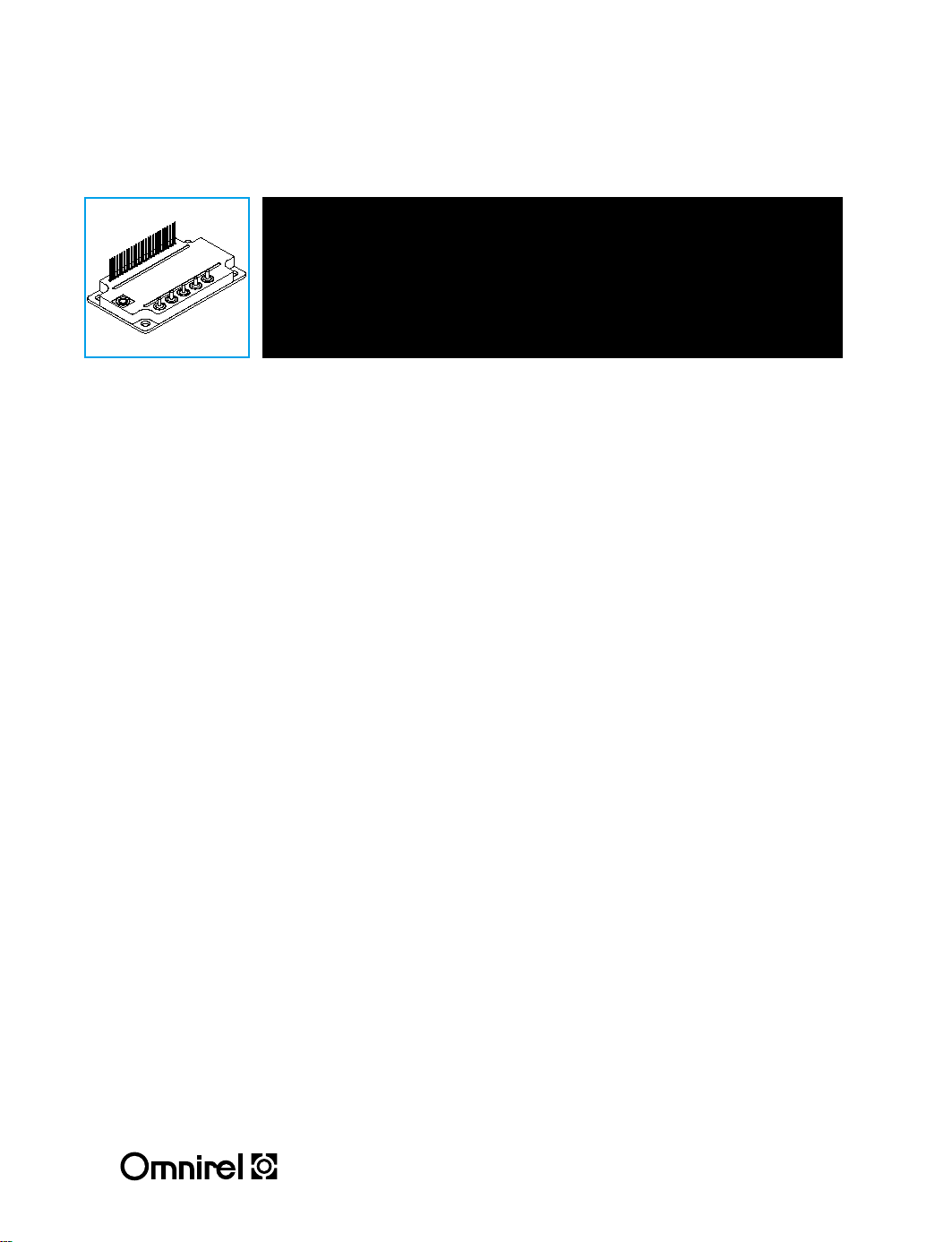
• Unique Lightweight Hermetic Ceramic-to-Metal Sealed Module (CERMOD
• (4.255" x 2.475" x .74")
TM
)
OM9369CM
APPLICATIONS
• Fans and Pumps
• Hoists
• Actuator Systems
DESCRIPTION
The OM9369CM is one of a series of versatile, integrated three-phase brushless DC motor
controller/driver subsystems housed in a CERMOD
quadrant speed controller for controlling/driving fans, pumps, and motors in applications which require
small size. Typical size brushless DC motors that the OM9369CM can effectively control range from
fractional HP up to several HP. The OM9369CM is ideal for use on DC distribution busses up to and
including 270Vdc. Many integral control features provide the user much flexibility in adapting the
OM9369CM to specific system requirements.
The small size of the complete subsystem is ideal for aerospace, military, and high-end industrial
applications.
8 10 R2
Supersedes 6 11 R1
TM
. The OM9369CM is best used as a two
OM9369CM
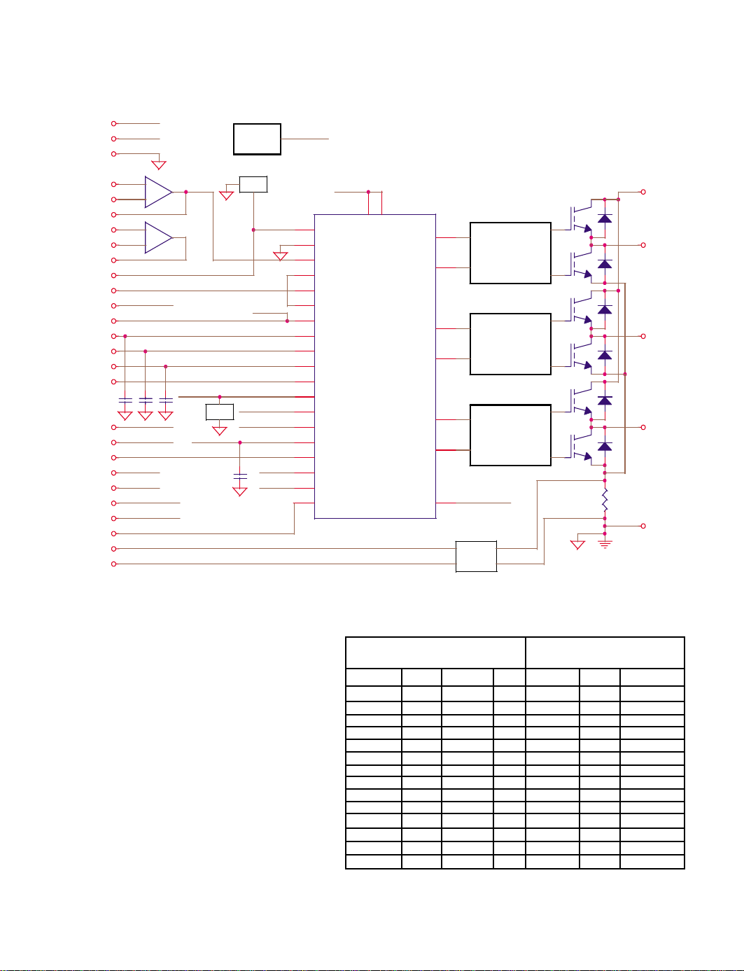
SIMPLIFIED BLOCK DIAGRAM
VCC (1)
Delay (2)
Ground (20)
EA1+ (5)
EA1- (3)
EA1_Out (9)
EA2+ (4)
EA2- (7)
EA2_Out (8)
Osc (11)
PWM_In (10)
SStart (19)
+5V_Ref (6)
Hall_1 (23)
Hall_2 (22)
Hall_3 (21)
Direction (25)
Quad_Sel (15)
OV_Coast (18)
I_Sense (12)
ISH (13)
ISL (14)
Tach_Out (16)
RC_Brake (17)
Speed_In (24)
CSH (26)
CSL (27)
Vcc
Delay Delay
+
-
+
-
SStart
RC_Brake
Quad_Sel
OV_Coast
ISH
ISL
RC_Brake
SStart
R/C
Startup
Circuit
R/C
V_Ref
Quad_Sel
OV_Coast
ISH
ISL
V_Ref
25
15
1
27
26
28
2
8
9
10
6
21
22
23
24
3
4
5
7
RC_OSC
GND
E/A_IN(+)
E/A_OUT
PWM_IN
E/A_IN(-)
VREF
H1
H2
H3
DIR
RC_BRAKE
QUAD_SEL
OV_COAST
SSTART
ISENSE
ISENSE_1
ISENSE_2
SPEED_IN
UC1625
Vcc
11
19
VCC
PWR_VCC
TACH_OUT
PUA
PDA
PUB
PDB
PUC
PDC
18
14
17
13
16
12
20
High-Side/
Low-Side
Drivers
with Bootstrap
and Charge Pump
High-Side/
Low-Side
Drivers
with Bootstrap
and Charge Pump
High-Side/
Low-Side
Drivers
with Bootstrap
and Charge Pump
Tach_OutTach_Out
R_Sense
V_Motor (B)
Phase_A (E)
Phase_B (D)
Phase_C (C)
Pwr_Gnd (A)
Filter
COMMUTATION TRUTH TABLE
This table shows the Phase Output state versus
the state of the Hall-Effect and Direction Inputs.
Please note that the OM9369CM Hall-Effect
Inputs are Grey-encoded; that is, only one input
is allowed to change from one input state to
another at a time.
The commutation coding shown reflects HallEffect sensors that are spaced at 120°
mechanical increments. Also, internal
protection logic disables all three Phase
Outputs when the Hall-Effect Inputs are set to
an illegal condition (i.e. all logic low or all logic
high).
DIGITAL INPUTS PHASE OUTPUTS
Dir H1 H2 H3 A B C
1 0 0 1 Hi-Z Sink Source
1 0 1 1 Sink Hi-Z Source
1 0 1 0 Sink Source Hi-Z
1 1 1 0 Hi-Z Source Sink
1 1 0 0 Source Hi-Z Sink
1 1 0 1 Source Sink Hi-Z
0 1 0 1 Sink Source Hi-Z
0 1 0 0 Sink Hi-Z Source
0 1 1 0 Hi-Z Sink Source
0 0 1 0 Source Sink Hi-Z
0 0 1 1 Source Hi-Z Sink
0 0 0 1 Hi-Z Source Sink
X 0 0 0 Hi-Z Hi-Z Hi-Z
X 1 1 1 Hi-Z Hi-Z Hi-Z
2.1 - 2

OM9369CM
ABSOLUTE MAXIMUM RATINGS
Motor Supply Voltage, Vm.................................................. 300 Vdc
Peak Motor Supply Voltage V
Average Phase Output Current, Io ................................... 25 Amperes DC*
Peak Phase Output Current, Iom................................... 50 Amperes Peak**
Control Supply Voltage, V
cc
Logic Input Voltage (Note 1) ............................................ -0.3 V to +8 V
Reference Source Current ................................................ -30 mAdc
Error Amplifier Input Voltage Range, (EA1+/EA1-) ....................-0.3 Vdc to 10 Vdc
Error Amplifier Output Current .............................................. ±8 mAdc
Spare Amplifier Input Voltage (EA2+/EA2-) ...........................-0.3 Vdc to 10 Vdc
Spare Amplifier Output Current ............................................. ±8 mAdc
Current Sense Amplifier Input Voltage (ISH/ISL) ....................... -0.3 V to +6 Vdc
Current Sense Amplifier Output Current.....................................±10 mAdc
Tachometer Output Current................................................±10 mAdc
PWM Input Voltage ..............................................-0.3 Vdc to +6 Vdc
Operating Junction Temperature .....................................-55°C to +150° C
Storage Temperature Range........................................-65° C to +150° C
Power Switch Junction-to-Case Thermal Resistance, Rθ
Package Isolation Voltage .................................................600 Vrms
Lead Soldering Temperature .............300°C, 10 seconds maximum, 0.125” from case
* Tcase = 25° C
** Tcase = 25° C, Maximum pulse width = 10mSec
........................................... 500 Vdc
m pK
................................................... +18 V
jc......................0.48°C/W
RECOMMENDED OPERATING CONDITIONS (Tcase = 25° C)
Motor Power Supply Voltage, Vm ......................................... +270Vdc
Average Phase Output Current, I
With Internal Current Sense Resistor (Note 2)
Each Power Switch .............................................25 A
Control Supply Voltage, V
cc
Logic Low Input Voltage, Vil........................................... 0.8 Vdc (max)
Logic High Input Voltage, Vih........................................... 2.0 Vdc (min)
Note 1: Logic Inputs: Direction, Hall Inputs (H1...H3) Overvoltage - Coast, Speed, and Quad Select.
Note 2: The internal 5mΩ current sense resistor is limited to 6 Wdc power dissipation. Other values are available.
Please contact the factory for more information.
O
............................................ 15Vdc ±10%
2.1 - 3

ELECTRICAL CHARACTERISTICS
PARAMETER SYMBOL CONDITIONS (NOTE 1) MIN. TYP. MAX. UNITS
Power Output Section
IGBT Leakage Current I
IGBT c-e Saturation Voltage Vce(sat) Ic = 50Adc 3.2 V
Diode Leakage Current I
Diode Forward Voltage V
Diode Reverse Recovery Time trr Io= 1A, di/dt = -100A/usec, 50 ns
Control Section
Control Supply Current Icc Vcc over operating range 100 mA
Control Turn-On Threshold Vcc(+) Tc over operating range 9.45 V
Driver Turn-On Threshold Vcc(+) Tc over operating range 13.0 V
Reference Section
Output Voltage Vr
Output Voltage Vr
Output Current Io --- --- 30 mA
Load Regulation Iload = 0mA to -20mA -40 -5 mV
Short Circuit Current Isc Tc over operating range 50 100 150 mA
Error Amplifier / Spare Amplifier Sections
EA1 / EA2 Input Offset Current Ios V(pin 3) = V(pin 5) = 0V -30 -3 0 nA
EA1 / EA2 Input Bias Current Iin V(pin 3) = V(pin 5) = 0V -50 -45 0 nA
Input Offset Voltage Vos 0V < Vcommon-mode < 3V 7 mV
Amplifier Output Voltage Range -- 0 6 V
PWM Comparator Section
PWM Input Current Iin V(pin 10) = 2.5V 0 3.0 30 uA
Current-Sense Amplifier Section
ISH / ISL Input Current Iin V(pin 13) = V(pin 14) = 0V -850 -320 0 uA
Input Offset Current Ios V(pin 13) = V(pin 14) = 0V +/-2 +/-12 uA
Peak Current Threshold Voltage Vpk V(pin 13) = 0V, V(pin 14) 0.14 0.20 0.26 V
Over Current Threshold Voltage Voc V(pin 13) = 0V, V(pin 14) 0.26 0.30 0.36 V
ISH / ISL Input Voltage Range -- (Note 2) -1 2 V
Amplifier Voltage Gain Av V(pin 13) = 0.3V, V(pin 14) 1.75 1.95 2.15 V/V
Amplifier Level Shift -- V(pin 13) = V(pin 14) = 0.3V 2.4 2.5 2.65 V
Logic Input Section
H1, H2, H3 Low Voltage Threshold Vil Tc over operating range 0.8 1.0 1.2 V
H1, H2, H3 High Voltage Threshold Vih Tc over operating range 1.6 1.9 2.0 V
H1, H2, H3 Input Current Iin Tc over operating range, -400 -250 -120 uA
Quad Select / Direction
Threshold Voltage Vth Tc over operating range 0.8 1.4 2.0 V
Quad Select Voltage Hysteresis Vh 70 mV
Direction Voltage Hysteresis Vh 0.6 V
Quad Select Input Current Iin -30 50 150 uA
Direction Input Current Iin -30 -1 30 uA
Overvoltage / Coast Input Section
Overvoltage / Coast Inhibit
Threshold Voltage Vth Tc over operating range 1.65 1.75 1.85 V
Overvoltage / Coast Restart
Threshold Voltage Vth Tc over operating range 1.55 1.65 1.75 V
Overvoltage / Coast Hysteresis Voltage Vh 0.05 0.10 0.15 V
Overvoltage / Coast Input Current Iin -10 -1 0 uA
ces
r
ef
ef
Vce = 600Vdc 300 uA
V
= 0V
ge
V
= 15V
ge
Vr= 600Vdc 100 uA
If= 37A 1.7 V
f
Vr = 30V
Tc over operating range 4.7 5.0 5.3 V
V(pin 4) = V(pin 7) = 0V
V(pin 4) = V(pin 7) = 0V
Varied to Threshold
Varied to Threshold
= 0.5V to 0.7V
V(pin 21, 22 or 23) = 0Vdc
4.9 5.0 5.1 V
2.1 - 4
OM9369CM

OM9369CM
Parameter Symbol Conditions (Note 1) MIN. TYP. MAX. Units
Soft-Start Section
Soft-Start Pull-Up Current Ip V(pin 19) = 0V -16 -10 -5 uA
Soft-Start Discharge Current Id V(pin 19) = 2.5V 0.1 0.4 3.0 mA
Soft-Start Reset Threshold Voltage Vth 0.1 0.2 0.3 V
Tachometer/Brake Section
Tachometer Output High Level Voh
Tachometer Output Low Level Vol
Tachometer On-Time ton 85 100 140 us
Tachometer On-Time Variation -Brake/Tach Timing Input Current Iin V (pin 17) = oV -4.0 -1.9 mA
Brake/Tach Timing
Threshold Voltage Vth
Brake/Tach Timing
Voltage Hysteresis Vh 0.09 V
Speed Input Threshold Voltage Vth Tc over operating range 220 257 290 mV
Speed Input Current Iin -30 -5 30 uA
Oscillator Section
Oscillator Frequency fo Measured at pin 11 13.5 14.8 20.0 kHz
Tc over operating range 4.7 5.0 5.3 V
(Pin 16) 10kΩ to 2.5 V
Tc over operating range
(Pin 16) 10kΩ to 2.5 V 0.2 V
Tc over operating range 0.1 %
Tc over operating range 0.8 1.0 1.2 V
SPECIFICATION NOTES:
1. All parameters specified for Ta = 25°C, Vcc = 15Vdc, Rosc = 75K
are sourced by (flow from) the pin under test.
2. Either ISH or ISL may be driven over the range shown.
3. Bold parameters tested at -55°C, 25°C, 125°C.
PINOUT
PIN# NAME PIN# NAME
1 VCC 24 Speed Input
2 Delay 25 Direction Input
3 EA1 “-” Input 26 CSH
4 EA2 “+” Input 27 CSL
5 EA1 “+” Input 28 (No Connection)
6 +5V Reference Output A Motor Return
7 EA2 “-” Input B Vmotor
8 EA2 Output C Phase C Output
9 EA1 Output D Phase B Output
10 PWM Input E Phase A Output
11 Oscillator Timing Input (Base) (No Connection)
12 Isense
13 ISH
14 ISL
15 Quad Select Input
16 Tachometer Output
17 Brake/Tach Timing Input
18 Overvoltage/Coast Input
19 Soft-Start Input
20 Ground
21 H3 Input
22 H2 Input
23 H1 Input
Ω (to Vref), Cosc = 1800 pF, and all Phase Outputs unloaded (Ta ~ Tj). All negative currents shown
2.1 - 5

PIN DESCRIPTIONS / FUNCTIONALITY
VCC (Pin 1) -- The Vcc Supply input provides bias
voltage to all of the internal control electronics within
the OM9369CM, and should be connected to a
nominal +15Vdc power source. High frequency
bypass capacitors (10uF polarized in parallel with
0.1uF ceramic are recommended) should be
connected as close as possible to pin 1 and Ground
(pin 20).
DELAY (Pin 2) -- This pin must be connected to the
Brake/Tach Timing Input pin (pin 17) to ensure that
the high-side bootstrap capacitors are charged
during initial startup.
ERROR AMPLIFIER (EA1- Input, Pin 3; EA1+
Input, Pin 5; EA1 Output, Pin 9) -- The Error
Amplifier is an uncommitted LM158-type operational
amplifier, providing the user with many external
control loop compensation options. This amplifier is
compensated for unity gain stability, so it can be
used as a unity gain input buffer to the internal PWM
comparator when pin 3 is connected to pin 9. The
output of the Error Amplifier is internally connected
to the PWM comparator's "-" input, simplifying
external layout connections.
+5V REFERENCE OUTPUT (Pin 6) -- This output
provides a temperature-compensated, regulated
voltage reference for critical external loads. It is
recommended that this pin be used to power the
external Hall-effect motor position sensors. By
design, the +5V reference must be in regulation
before the remainder of the control circuitry is
activated. This feature allows the Hall-effect sensors
to become powered and enabled before any Phase
Output is enabled in the OM9369CM, preventing
damage at turn-on. High-frequency bypass
capacitors (10uF polarized in parallel with 0.1uF
ceramic are recommended) should be connected as
close as possible to pin 5 and Ground (pin 20).
SPARE AMPLIFIER (EA2- Input, Pin 7; EA2+
Input, Pin 4; EA2 Output, Pin 8) -- The Spare
Amplifier is an uncommitted LM158-type operational
amplifier, and in addition to the internal error
amplifier, provides the user with additional external
control loop compensation options. This amplifier is
also compensated for unity gain stability and it can
be used as a unity gain input buffer when pin 7 is
connected to pin 8. If the Spare Amplifier is unused,
pin 4 should be connected to Ground, and pin 7
should be connected to pin 8.
PWM INPUT (Pin 10) -- This pin is connected to the
"+" input of the internal PWM comparator. The PWM
output clears the internal PWM latch, which in turn
OM9369CM
commands the Phase Outputs to chop. For voltagemode control systems, pin 10 may be connected to the
Oscillator Timing Input, pin 11.
OSCILLATOR TIMING INPUT (Pin 11) -- The Oscillator
Timing Input sets a fixed PWM chopping frequency by
means of an internal resistor (Rosc), whose value is set
to 75kΩ, connected from pin 11 to the +5V Reference
Output, and an internal capacitor (Cosc), whose value
is 1800pF, connected from pin 11 to Ground. In custom
applications, the recommended range of values for
Rosc is 10kΩ to 100kΩ, and for Cosc is 0.001uF to
0.01uF, and the maximum operating frequency should
be kept below 20kHz. The approximate oscillator
frequency is:
2
fo = (Rosc x Cosc)
The voltage waveform on pin 11 is a ramp whose
magnitude is approximately 1.2Vp-p, centered at
approximately 1.6Vdc. In addition to the voltage-mode
PWM control, pin 11 may be used for slope
compensation in current-mode control applications.
ISENSE (Pin 12) -- This pin is connected to the output
of the internal current-sense amplifier. It drives a peakcurrent (cycle-by-cycle) comparator which controls
Phase Output chopping, and a fail-safe current
comparator which, in the event of an output overcurrent
condition, activates the soft-start feature and disables
the Phase Outputs until the overcurrent condition is
removed. The magnitude of the voltage appearing at pin
12 is dependent upon the voltages present at the
current-sense amplifier inputs, ISH and ISL:
V(Isense) = 2.5V + [2 x ABS (ISH - ISL)] [Volts]
CURRENT SENSE INPUTS (ISH, Pin 13; ISL, pin 14)
-- These inputs to the current-sense amplifier are
interchangeable and they can be used as differential
inputs. The differential voltage applied between pins 13
and 14 should be kept below +/-0.5Vdc to avoid
saturation.
QUAD SELECT INPUT (Pin 15) -- This input is used to
set the OM9369CM in a half control or full control
chopping regime. When driven with a logic low level, the
OM9369CM is in the half control mode, whereby only
the three lower (pull-down) power switches associated
with the Phase Outputs are allowed to chop. Alternately,
when driven with a logic high level, the OM9369CM is in
the full control mode, where all six power switches (pullup and pull-down) associated with the Phase Outputs
are chopped by the PWM. During motor braking,
changing the logic state of the Quad Select Input has no
effect on the operation of the OM9369CM.
2.1 - 6
[Hz]

OM9369CM
TACHOMETER OUTPUT (Pin 16) -- This output
provides a fixed width 5V pulse when any Hall-effect
Input (1, 2 or 3) changes state. The pulse width of the
Tachometer Output is set internally in the OM9369CM
to 113µs (nominal). The average value of the output
voltage on pin 16 is directly proportional to the motor's
speed, so this output may be used (with an external
averaging filter) as a true tachometer output, and fed
back to the Speed Input (pin 24) to sense the actual
motor speed.
Note: Whenever pin 16 is high, the internal Hall-effect
position latches are inhibited (i.e. "latched"), to reject
noise during the chopping portion of the commutation
cycle, and this makes additional commutations
impossible. This means that in order to prevent false
commutation at a speed less than the desired
maximum speed, the highest speed as observed at the
Tachometer Output should be set above the expected
maximum value.
BRAKE / TACH TIMING INPUT (Pin 17) -- The
Brake/Tach Timing Input is a dual-purpose input.
Internal to the OM9369CM are timing components tied
from pin 17 to Ground (a 51kΩ resistor and a 3300pF
capacitor). These components set the minimum pulse
width of the Tachometer Output to 113µs, and this time
may be adjusted using external components,
according to the equation:
T(tach) = 0.67 x (Ct+ 3300pf) x
The recommended range of external resistance (to
Ground) is 15kΩ to ∞, and the range of external
capacitance (to Ground) is 0pF to 0.01uF. With each
Tachometer Output pulse, the capacitor tied to pin 17
is discharged from approximately 3.33V to
approximately 1.67V by an internal timing resistor. The
Brake / Tach Timing Input has another function. If this
pin is pulled below the brake threshold voltage, the
OM9369CM will enter the brake mode. The brake
mode is defined as the disabling of all three high-side
(pull-up) drivers associated with the Phase Outputs,
and the enabling of all three low-side (pull-down)
drivers.
OVERVOLTAGE / COAST INPUT (Pin 18) -- This
input may be used as a shutdown or an enable/disable
input to the OM9369CM. Also, since the switching
inhibit threshold is so tightly defined, this input can be
directly interfaced with a resistive divider which senses
the voltage of the motor supply, Vm, for overvoltage
conditions. A high level (greater than the inhibit
threshold) on pin 18 causes the coast condition to
occur, whereby all Phase Outputs revert to a Hi-Z state
and any motor current which flowed prior to the
Overvoltage / Coast command is commutated via the
power "catch" rectifiers associated with each Phase
Output.
2.1 - 7
Rt x 51kΩ )(µs)
(
Rt + 51kΩ
SOFT-START INPUT (Pin 19) -- The Soft-Start input is
internally connected to a 10µA (nominal) current source,
the collector of an NPN clamp/discharge transistor, and a
voltage comparator whose soft-start/restart threshold is
0.2Vdc (nominal). An external capacitor is connected
from this pin to Ground (pin 20). Whenever the Vcc
supply input drops below the turn-on threshold,
approximately 9Vdc, or the sensed current exceeds the
over-current threshold, approximately 0.3V at the current
sense amplifier, the soft-start latch is set. This drives the
NPN clamp transistor which discharges the external softstart capacitor. When the capacitor voltage drops below
the soft-start/restart threshold and a fault condition does
not exist, the soft-start latch is cleared; the soft-start
capacitor charges via the internal current source.
In addition to discharging the soft-start capacitor, the
clamp transistor also clamps the output of the error
amplifier internal to the controller IC, not allowing the
voltage at the output of the error amplifier to exceed the
voltage at pin 19, regardless of the inputs to the amplifier.
This action provides for an orderly motor start-up either at
start-up or when recovering from a fault condition.
GROUND (Pin 20) -- The voltages that control the
OM9369CM are referenced with respect to this pin. All
bypass capacitors, timing resistors and capacitors, loop
compensation components, and the Hall-effect filter
capacitors must be referenced as close as possible to pin
20 for proper circuit operation. Additionally, pin 20 must
be connected as close as physically possible to the Motor
Return, pin A.
HALL-EFFECT INPUTS (H1, Pin 23; H2, Pin 22; H3, Pin
21) -- Each input has an internal pull-up resistor to the
+5V Reference. Each input also has an internal 180pF
noise filter capacitor to Ground. In order to minimize the
noise which may be coupled from the motor commutation
action to these inputs, it is strongly recommended that
additional external filter capacitors, whose value is in the
range of 2200pF, be connected from each Hall-Effect
Input pin to Ground. Whatever capacitor value is used,
the rise/fall times of each input must be guaranteed to be
less than 20us for proper tachometer action to occur.
Motors with 60 degree position sensing may be used if
one or two of the Hall-effect sensor signals is inverted
prior to connection to the Hall-Effect Inputs.
SPEED INPUT (Pin 24) - This pin is connected to the “+”
input of a voltage comparator, whose threshold is
0.25Vdc. As long as the Speed Input is less than 0.25V,
the direction latch is transparent. When the Speed Input
is greater than 0.25V, then the direction latch inhibits all
changes in direction. It is recommended, especially while
operating in the half control mode, that the Tachometer
Output is connected to the Speed Input via a low-pass
filter, such that the direction latch is transparent only
when the motor is spinning very slowly. In this case,
the motor has too little stored energy to damage the
power devices during direction reversal.

DIRECTION INPUT (Pin 25) - This input is used to
select the motor direction. This input has an internal
protection feature: the logic-level present on the
Direction Input is first loaded into a direction latch, then
shifted through a two-bit shift register before
interfacing with the internal output phase driver logic
decoder. Also, protection circuitry detects when the
input and the output of the direction latch or the 2-bit
shift register are different, and inhibits the Phase
Outputs (i.e. Hi-Z) during those times. This feature
may be used to allow the motor to coast to a safe
speed before a direction reversal takes place. Power
stage cross-conduction (current "shoot-through" from
Vmotor to Ground through simultaneously enabled
pull-up and pull-down drivers) is prevented by the shift
register as it is clocked by the PWM oscillator, so that
a fixed delay of between one and two PWM oscillator
clock cycles occurs. This delay or "dead-time"
guarantees that power-stage cross-conduction will not
occur.
CURRENT SENSE OUTPUTS (CSH, Pin 26; CSL,
Pin 27) - The Current Sense Outputs produce a
differential voltage equal to the motor current times the
sense resistance value (5mΩ nominal). There is an
internal 1000pF filter capacitor across pins 26 and 27,
and two 100Ω series resistors, one between each pin
and each end of the current sense resistor. To
configure the current sense amplifier for cycle-by-cycle
current limiting and/or overcurrent protection, connect
pin 26 to pin 13 (ISH) and pin 27 to pin 14 (ISL).
MOTOR RETURN (Pin A) - This pin is connected to
the most negative terminal of the motor supply (Vm-).
This connection is electrically isolated from the logic
Ground internal to the OM9369CM package to
minimize, if not eliminate, noise on the logic ground.
The connection to the logic ground is made by the user
external to the package (refer to Ground (pin 20)). In
order to minimize packaging losses and parasitic
effects, it is essential that both of these pins be firmly
connected to the motor supply ground, with as short a
connection as physically possible.
OM9369CM
PHASE OUTPUTS (Phase A, Pin E; Phase B, Pin D;
Phase C, Pin C) -- These outputs are connected to
either Vmotor via the pull-up driver or Source via the
pull-down driver, depending upon the Hall-Effect and
Direction Inputs (see Commutation Truth Table). The
pin associated with each Phase Output must be
connected to one of the three phases of the motor
driven by the OM9369CM.
V
MOTOR
positive terminal of the motor supply (Vm+). For
proper operation, this pin must be connected
externally with a low impedance power bus. The
V
motor
adequately voltage-rated ceramic capacitor, 0.1µF
(typical), and a low-ESR electrolytic capacitor, whose
capacitance value can be selected by the following:
10µF-per-Ampere of average motor current from
V
motor
Note: All connections, including the power bus
capacitor connections, must be made as close as
possible to the V
minimize parasitic effects.
PACKAGE AND SCREENING OPTIONS
The OM9369CM is offered in a hermetic CERMOD
CM-1LP, as shown in Figure 1.
The OM9369CM operates over the full military
temperature range of -55°C to +125°C, and is
available with two standard screening levels, CMP,
limited screening, and CMB, MIL-STD-883 screening.
The screening levels for the CMP and CMB versions
are listed in the table below. All tests and inspections
are in accordance with those listed in MIL-STD-883.
Note: For lower bus voltages and MOSFET versions
in a CERMOD
(Pin B) - This pin is connected to the most
power bus should be bypassed with an
to Motor Return.
and Motor Return pins to
motor
TM
package contact the factory.
TM
Table 1
,
Test/Inspection CMB CMP
Precap Visual Inspection 100% 100%
Temperature Cycle 100% N.A.
Mechanical Shock 100% N.A.
Hermeticity (Fine and Gross Leak) 100% 100%
Pre Burn-In Electrical 100% N.A.
Burn-In (160 hours) 100% N.A.
Final Electrical Test -55°C, +25°C, +25°C
+125°C
Group A Testing 100% N.A.
Final Visual Inspection 100% 100%
2.1 - 8

OM9369CM
APPLICATIONS
Modes of Operation
Figures 2 and 3, shown on the following pages,
provide schematic representations of typical voltagemode and current-mode applications for the
OM9369CM controller/driver.
Figure 2 represents the implementation of a typical
voltage-mode controller for velocity control. Avoltage
or speed command is applied to the non-inverting
input of the error amplifier which is configured as a
voltage follower. The output of the error amplifier is
compared to a pulse width modulated ramp, and since
motor speed is nearly proportional to the average
phase output voltage, the speed is controlled via duty
cycle control. If a speed feedback loop is required, the
tachometer output can be connected to the inverting
input of the error amplifier via a loop compensation
network.
Figure 2 also shows the implementation of the cycleby-cycle current limit/overcurrent protection feature of
the OM9369CM. The load current is monitored via the
controller’s internal sense resistor. The current sense
signal is filtered and fed into the current sense
amplifier where the absolute value of ISH-ISL is
MECHANICAL OUTLINE
multiplied by two and biased up by 2.5 volts.
The output of the current sense amplifier is compared
to a fixed reference, thus providing cycle-by-cycle
current limiting and/or overcurrent protection as
necessary. The typical peak current threshold (ISHISL) is 0.20 volts; the typical over current threshold
(ISH-ISL) is 0.30 volts.
Figure 3 represents the implementation of a typical
current-mode controller for torque control. The load
current is monitored via the controller’s internal sense
resistor. The current sense signal is filtered and fed
into the current sense amplifier where the absolute
value of ISH-ISL is multiplied by two and biased up by
2.5 volts. Besides the implementation of the cycle-bycycle current limit/overcurrent protection feature of the
OM9369CM discussed in the preceding paragraph, the
output of the current sense amplifier is fed into the error
amplifier which is configured as a differential amplifier.
An error signal representing the difference between the
current command input and the value of the amplified
current sense signal is produced. Then it is compared
to a pulse width modulated ramp and since torque is
nearly proportional to the average phase output
current, the torque is controlled via duty cycle control.
Fig 1: Mechanical Outline CM-1LP CERMOD
2.1 - 9
TM

+15V
3.24k
COMMAND
1k
1.50k
FROM MOTOR HALL SENSORS
H2
H1
4700pF
10uF
+
.1uF 10k
232
232
.1uF
.1uF
1
VCC
2
DELAY
3
EA1-
4
EA2+
5
EA1+
6
+5V_REF
7
EA2-
8
EA2_OUT
9
EA1_OUT
10
PWM_IN
11
OSC
12
I_SENSE
13
ISH
14
ISL
15
QUAD_SEL
16
TACH_OUT
17
RC_BRAKE
18
OV_COAST
19
SOFT_START
20
GROUND
21
H3_HALL_INPUT
22
H2_HALL_INPUT
23
H1_HALL_INPUT
24
SPEED_IN
25
DIRECTION
26
CSH
27
CSL
28
N/C
OM9369CM
PHASE_A_OUT
PHASE_B_OUT
PHASE_C_OUT
V_MOTOR
MOTOR_RETURN
OM9369CM
E
D
C
B
C_BUS
+
A
V_Motor
C_FILT
HALL SENSORS
H1H3
H2
H3
MOTOR
Fig 2: Implementation of a Voltage-Mode Controller
CURRENT_COMMAND
+15V
3.24k
35.6k
OFFSET
1k
3.24k
ROM MOTOR HALL SENSORS
H3
H2
H1
.26uF
1800pF
43k
4700pF
10uF
.1uF
+
1
VCC
2
DELAY
3
EA1-
4
EA2+
5
EA1+
6
+5V_REF
7
EA2-
8
EA2_OUT
9
EA1_OUT
10
2k
10k.1uF
.1uF
232
232
PWM_IN
11
OSC
12
I_SENSE
13
ISH
14
ISL
15
QUAD_SEL
16
TACH_OUT
17
RC_BRAKE
18
OV_COAST
19
SOFT_START
20
GROUND
21
H3_HALL_INPUT
22
H2_HALL_INPUT
23
H1_HALL_INPUT
24
SPEED_IN
25
DIRECTION
26
CSH
27
CSL
28
N/C
OM9369CM
PHASE_A_OUT
PHASE_B_OUT
PHASE_C_OUT
V_MOTOR
MOTOR_RETURN
E
D
C
B
C_BUS
+
A
V_Motor
C_FILT
H1
H2
H3
MOTOR
HALL SENSORS
Fig 3: Implementation of a Current-Mode Controller
2.1 - 10
 Loading...