

OM60N06SA
OM50N06SA
OM60N05SA
OM50N05SA
OM50N06ST
OM50N05ST
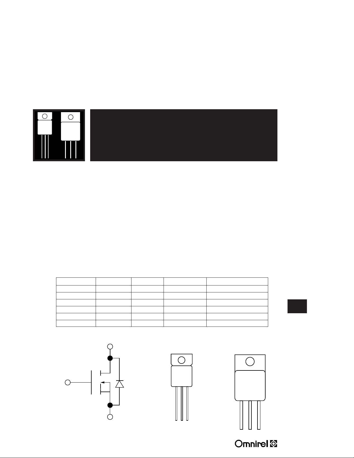
LOW VOLTAGE, LOW R
DS(on)
POWER MOSFETS
IN HERMETIC ISOLATED PACKAGE
50V And 60V Ultra Low R
Power MOSFETs In TO-257 And TO-254
Isolated Packages
FEATURES
• Isolated Hermetic Metal Packages
• Ultra Low R
• Low Conductive Loss/Low Gate Charge
• Available Screened To MIL-S-19500, TX, TXV And S Levels
• Ceramic Feedthroughs Available
DS(on)
DESCRIPTION
This series of hermetic packaged MOSFETs are ideally suited for low voltage
applications; battery powered voltage power supplies, motor controls, dc to dc
converters and synchronous rectification. The low conduction loss allows smaller
heat sinking and the low gate charge simpler drive circuitry.
DS(on)
MAXIMUM RATINGS (Per Device)
PART NO. VDS(V) R
OM60N06SA 60 .025 60 TO-254AA
OM50N06SA 60 .030 50 TO-254AA
OM50N06ST 60 .035 50 TO-257AA
OM60N05SA 50 .025 60 TO-254AA
OM50N05SA 50 .030 50 TO-254AA
OM50N05ST 50 .035 50 TO-257AA
SCHEMATIC T-3 PIN
Drain
Gate
Source
() ID(A) Package
DS(on)
CONNECTION
123
Pin 1: Drain
Pin 2: Source
Pin 3: Gate
CONNECTION
Pin 1: Drain
Pin 2: Source
Pin 3: Gate
M-PAK PIN
3.1
123
4 11 R1
Supersedes 3 02 R0
3.1 - 65
OM60N06SA - OM50N05ST
.144 DIA.
.050
.040
.260
.249
.685
.665
.800
.790
.545
.535
.550
.510
.045
.035
.550
.530
.150 TYP.
.150 TYP.
.005
.430
.410
.200
.190
.038 MAX.
.005
.120 TYP.
.537
.527
.665
.645
.420
.410
.150
.140
.750
.500
.100 TYP.
.035
.025
.045
.035
ABSOLUTE MAXIMUM RATINGS (TC= 25°C unless otherwise noted)
Parameter 60N06SA
V
DS
V
DGR
Drain-Source Voltage 60 60 50 50 V
Drain-Gate Voltage (RGS= 1 M ) 60 60 50 50 V
ID@ TC= 25°C Continuous Drain Current
ID@ TC= 100°C Continuous Drain Current
I
DM
Pulsed Drain Current
PD@ TC= 25°C Maximum Power Dissipation 100 100 100 100 W
PD@ TC= 100°C Maximum Power Dissipation 40 40 40 40 W
Junction-To-Case Linear Derating Factor
T
J
T
stg
Operating and
Storage Temperature Range
Lead Temperature (1/16" from case for 10 secs.) 300 300 300 300 °C
1 Pulse Test: Pulse width 300 µsec. Duty Cycle 1.5%.
2 Package Limited SA I
= 25 A, SC SC ID= 35 A @ 25 C
D
THERMAL RESISTANCE
R
Junction-to-Case 1.25 °C/W
thJC
PACKAGE LIMITATIONS
Parameters TO254AA TO-257AA Unit
I
Continuous Drain Current 25 15 A
D
Linear Derating Factor, Junction-to-Ambient .020 .015 W/°C
R
Thermal Resistance, Junction-to-Ambient (Free Air Operation) 50 65 °C/W
thJA
Linear Derating, Junction-to-Case 0.8 0.8 W/°C
50N06ST 50N05ST
50N05SA
2
2
1
1
55 50 55 50 A
37 33 37 33 A
220 200 220 200 A
.80 .80 .80 .80 W/°C
60N05SA
50N05SA
Units
-55 to 150 -55 to 150 -55 to 150 -55 to 150 °C
3.1
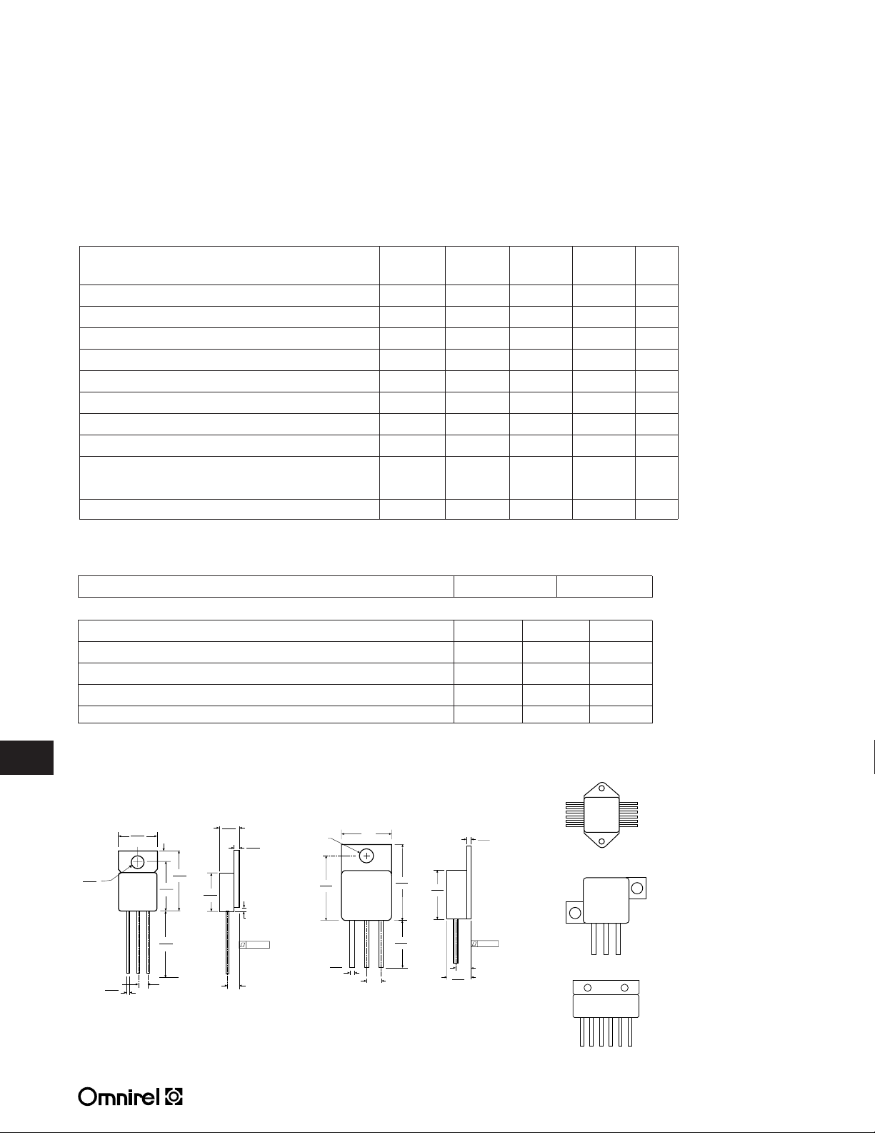
PACKAGE OPTIONS
T-3 MECHANICAL OUTLINE
Notes:
• Standard Products are supplied with glass feedthroughs. For ceramic feedthroughs, add the letter “C” to the
part number. Example - OMXXXXCSA.
• MOSFETs are also available in Z-Pak, dual and quad pak styles. Please call the factory for more information.
M-PAK MECHANICAL OUTLINE
MOD PAK
Z-TAB
6 PIN SIP
3.1 - 66

OM60N06SA - OM50N05ST
= 25°C)
J
= 25 V)
= 25°C,
J
DD
, V
AR
= I
D
I
non-repetitive,T
= 25°C unless otherwise specified)
C
Avalanche Current 50 A (repetitive or
Single Pulse Avalanche Energy 400 mJ (starting T
AS
AR
I
OM50N06SA (T
E
Avalanche Characteristics Min. Typ. Max. Units Test Conditions
= 100°C)
J
, d< 1%)
j max
by T
non-repetitive, T
Repetitive Avalanche Energy 100 mJ (pulse width limited
Avalanche Current 30 A (repetitive or
AR
AR
I
E
Electrical Characteristics - OFF
= 125°C
C
= 0
GS
= ±20 V
= Max. Rat.
= Max. Rat. x 0.8, T
= 250 µA, V
DS
GS
DS
D
= 0) 1000 µA V
GS
Drain-Source 60 V I
Zero Gate Voltage 250 µA V
Gate-Body Leakage ±100 nA V
Breakdown Voltage
Drain Current (V
(BR)DSS
DSS
GSS
I
V
I
= 10 V
GS
= 25 A
D
, V
, I
= 25 A
DS(on)max
= 250 µA
D
D
, I
GS
= 10 V, I
= V
DS
GS
= 0)
DS
Current (V
Gate Threshold Voltage 2 4 V V
Static Drain-Source On .028 V
DS(on)
GS(th)
R
V
Electrical Characteristics - ON*
DS(on)max
x R
x R
D(on)
D(on)
> I
> I
= 100°C
C
Resistance .056 T
= 25 V
DS
DS
DS
On State Drain Current 50 A V
Forward Transconductance 17 S V
Input Capacitance 2000 pF V
ies
fs
D(on)
C
I
g
Electrical Characteristics - Dynamic
= 10 V
GS
= 10 V
= 10 V
= 29 A
= 50 A
GS
D
D
GS
= 0
= 25 V, I
= 40 V, I
= 4.7 , V
= 50 , V
G
GS
Output Capacitance 1000 pF V
Reverse Transfer Capacitance 300 pF f = 1 mHz
oes
res
C
C
Electrical Characteristics - Switching On
G
DD
DD
R
Turn-On Time 45 nS V
Rise Time 90 nS R
Turn-On Current Slope 200 A/µS V
on
d(on)
r
t
(di/dt)
T
= 10 V
= 50 A, V
= 50 A
D
D
GS
= 40 V, I
= 40 V, I
= 50 , V
G
DD
DD
Total Gate Charge 45 nC V
Off Voltage Rise Time 160 nS V
Fall Time 90 nS R
g
r(Voff)
f
t
Q
T
Electrical Characteristics - Switching Off
= 0
= 150°C
GS
j
= 30 V, T
= 50 A, V
= 50 A, di/dt = 100 A/µs
R
SD
SD
V
Cross-Over Time 250 nS
Source Drain Current 50 A
Forward On Voltage 2 V I
Reverse Recovery Time 150 nS I
Reverse Recovery Charge 0.2 µC
Reverse Recovery Current 4 A
* Source Drain Current (pulsed) 200 A
cross
SD
SDM
I
t
I
Electrical Characteristics - Source Drain Diode
rr
SD
rr
RRM
I
*Pulsed: Pulse Duration 300µS, Duty Cycle 1.5%.
Q
V
t
= 25°C)
J
= 25 V)
= 25°C,
J
DD
, V
AR
= I
D
I
non-repetitive,T
= 25°C unless otherwise specified)
C
Avalanche Current 55 A (repetitive or
Single Pulse Avalanche Energy 520 mJ (starting T
AS
AR
I
OM60N06SA (T
E
Avalanche Characteristics Min. Typ. Max. Units Test Conditions
= 100°C)
J
, d< 1%)
j max
by T
non-repetitive, T
Repetitive Avalanche Energy 130 mJ (pulse width limited
Avalanche Current 34 A (repetitive or
AR
AR
I
E
Electrical Characteristics - OFF
= 125°C
C
= 0
GS
= ±20 V
= Max. Rat.
= Max. Rat. x 0.8, T
= 250 µA, V
DS
GS
DS
D
= 0) 1000 µA V
GS
Drain-Source 60 V I
Zero Gate Voltage 250 µA V
Gate-Body Leakage ±100 nA V
Breakdown Voltage
Drain Current (V
(BR)DSS
DSS
GSS
I
V
I
= 10 V
GS
= 30 A
D
, V
, I
= 30 A
DS(on)max
= 250 µA
D
D
, I
GS
= 10 V, I
= V
DS
GS
= 0)
DS
Current (V
Gate Threshold Voltage 2 4 V V
Static Drain-Source On .025 V
DS(on)
GS(th)
R
V
Electrical Characteristics - ON*
DS(on)max
x R
x R
D(on)
D(on)
> I
> I
= 100°C
C
Resistance .050 T
= 25 V
DS
DS
DS
On State Drain Current 55 A V
Forward Transconductance 16 S V
Input Capacitance 2500 pF V
ies
fs
D(on)
C
I
g
Electrical Characteristics - Dynamic
= 10 V
GS
= 10 V
= 10 V
= 55 A
= 55 A
D
D
GS
GS
= 0
= 25 V, I
= 40 V, I
= 50 , V
= 50 , V
G
GS
Output Capacitance 950 pF V
Reverse Transfer Capacitance 250 pF f = 1 mHz
oes
res
C
C
Electrical Characteristics - Switching On
G
DD
DD
R
Turn-On Time 110 nS V
Rise Time 300 nS R
Turn-On Current Slope 160 A/µS V
on
d(on)
r
t
(di/dt)
T
= 10 V
= 30 A, V
= 55 A
D
D
GS
= 25 V, I
= 40 V, I
= 50 , V
G
DD
DD
Total Gate Charge 65 nC V
Off Voltage Rise Time 160 nS V
Fall Time 160 nS R
g
r(Voff)
f
t
Q
T
Electrical Characteristics - Switching Off
= 0
= 150°C
GS
j
= 25 V, T
= 55 A, V
= 55 A, di/dt = 100 A/µs
R
SD
SD
V
Cross-Over Time 320 440 nS
Source Drain Current 55 A
Forward On Voltage 1.6 V I
Reverse Recovery Time 100 nS I
Reverse Recovery Charge .25 µC
Reverse Recovery Current 5 A
* Source Drain Current (pulsed) 200 A
cross
SD
SDM
I
t
I
Electrical Characteristics - Source Drain Diode
rr
SD
rr
RRM
I
V
t
*Pulsed: Pulse Duration 300µS, Duty Cycle 1.5%.
Q
3.1
3.1 - 67

3.1
OM60N06SA - OM50N05ST
OM50N06ST (T
= 25°C unless otherwise specified)
C
Avalanche Characteristics Min. Typ. Max. Units Test Conditions
Avalanche Current 50 A (repetitive or
I
AR
Single Pulse Avalanche Energy 400 mJ (starting TJ= 25°C,
E
AS
Repetitive Avalanche Energy 100 mJ (pulse width limited
E
AR
Avalanche Current 30 A (repetitive or
I
AR
Electrical Characteristics - OFF
Drain-Source 60 V ID= 250 µA, VGS= 0
V
(BR)DSS
Breakdown Voltage
Zero Gate Voltage 250 µA VDS= Max. Rat.
I
DSS
Drain Current (V
Gate-Body Leakage ±100 nA V
I
GSS
Current (V
Electrical Characteristics - ON*
Gate Threshold Voltage 2 4 V VDS= VGS, ID= 250 µA
V
GS(th)
Static Drain-Source On .033 VGS= 10 V, ID= 25 A
R
3.1 - 68
DS(on)
Resistance .066 T
On State Drain Current 50 A VDS> I
I
D(on)
Electrical Characteristics - Dynamic
Forward Transconductance 17 S VDS> I
g
fs
Input Capacitance 2000 pF VDS= 25 V
C
ies
Output Capacitance 1000 pF VGS= 0
C
oes
Reverse Transfer Capacitance 300 pF f = 1 mHz
C
res
Electrical Characteristics - Switching On
Turn-On Time 45 nS VDD= 25 V, ID= 29 A
T
d(on)
Rise Time 90 nS RG= 4.7 , VGS= 10 V
t
r
Turn-On Current Slope 200 A/µS VDD= 40 V, ID= 50 A
(di/dt)
on
Total Gate Charge 45 nC VDD= 40 V, ID= 50 A, VGS= 10 V
Q
g
Electrical Characteristics - Switching Off
Off Voltage Rise Time 160 nS VDD= 40 V, ID= 50 A
T
r(Voff)
Fall Time 90 nS RG= 50 , VGS= 10 V
t
f
Cross-Over Time 250 nS
t
cross
Electrical Characteristics - Source Drain Diode
Source Drain Current 50 A
I
SD
* Source Drain Current (pulsed) 200 A
I
SDM
Forward On Voltage 2 V ISD= 50 A, VGS= 0
V
SD
Reverse Recovery Time 150 nS ISD= 50 A, di/dt = 100 A/µs
t
rr
Reverse Recovery Charge 0.2 µC
Q
rr
Reverse Recovery Current 4 A
I
RRM
= 0) 1000 µA VDS= Max. Rat. x 0.8, TC= 125°C
GS
= 0)
DS
*Pulsed: Pulse Duration 300µS, Duty Cycle 1.5%.
non-repetitive,T
= IAR, VDD= 25 V)
I
D
, d< 1%)
by T
j max
non-repetitive, T
= ±20 V
GS
= 100°C
C
x R
D(on)
x R
D(on)
= 50 , VGS= 10 V
R
G
= 30 V, Tj= 150°C
V
R
= 25°C)
J
= 100°C)
J
DS(on)max
DS(on)max
, VGS= 10 V
, ID= 25 A
OM60N05SA (T
= 25°C unless otherwise specified)
C
Avalanche Characteristics Min. Typ. Max. Units Test Conditions
Avalanche Current 55 A (repetitive or
I
AR
Single Pulse Avalanche Energy 520 mJ (starting TJ= 25°C,
E
AS
Repetitive Avalanche Energy 130 mJ (pulse width limited
E
AR
Avalanche Current 34 A (repetitive or
I
AR
non-repetitive,T
= IAR, VDD= 25 V)
I
D
, d< 1%)
by T
j max
non-repetitive, T
Electrical Characteristics - OFF
Drain-Source 50 V ID= 250 µA, VGS= 0
V
(BR)DSS
Breakdown Voltage
Zero Gate Voltage 250 µA VDS= Max. Rat.
I
DSS
Drain Current (V
Gate-Body Leakage ±100 nA V
I
GSS
Current (V
Electrical Characteristics - ON*
Gate Threshold Voltage 2 4 V VDS= VGS, ID= 250 µA
V
GS(th)
Static Drain-Source On .025 VGS= 10 V, ID= 30 A
R
DS(on)
Resistance .050 T
On State Drain Current 55 A VDS> I
I
D(on)
Electrical Characteristics - Dynamic
Forward Transconductance 16 S VDS> I
g
fs
Input Capacitance 2500 pF VDS= 25 V
C
ies
Output Capacitance 950 pF VGS= 0
C
oes
Reverse Transfer Capacitance 250 pF f = 1 mHz
C
res
Electrical Characteristics - Switching On
Turn-On Time 110 nS VDD= 25 V, ID= 55 A
T
d(on)
Rise Time 300 nS RG= 50 , VGS= 10 V
t
r
Turn-On Current Slope 160 A/µS VDD= 40 V, ID= 55 A
(di/dt)
on
Total Gate Charge 65 nC VDD= 25 V, ID= 30 A, VGS= 10 V
Q
g
Electrical Characteristics - Switching Off
Off Voltage Rise Time 160 nS VDD= 40 V, ID= 55 A
T
r(Voff)
Fall Time 160 nS RG= 50 , VGS= 10 V
t
f
Cross-Over Time 320 nS
t
cross
Electrical Characteristics - Source Drain Diode
Source Drain Current 55 A
I
SD
* Source Drain Current (pulsed) 200 A
I
SDM
Forward On Voltage 1.6 V ISD= 55 A, VGS= 0
V
SD
Reverse Recovery Time 100 nS ISD= 55 A, di/dt = 100 A/µs
t
rr
Reverse Recovery Charge .25 µC
Q
rr
Reverse Recovery Current 5 A
I
RRM
= 0) 1000 µA VDS= Max. Rat. x 0.8, TC= 125°C
GS
= 0)
DS
= ±20 V
GS
= 100°C
C
x R
D(on)
x R
D(on)
= 50 , VGS= 10 V
R
G
= 25 V, Tj= 150°C
V
R
DS(on)max
DS(on)max
*Pulsed: Pulse Duration 300µS, Duty Cycle 1.5%.
= 25°C)
J
= 100°C)
J
, VGS= 10 V
, ID= 30 A

OM50N05SA (T
= 25°C unless otherwise specified)
C
Avalanche Characteristics Min. Typ. Max. Units Test Conditions
Avalanche Current 50 A (repetitive or
I
AR
Single Pulse Avalanche Energy 400 mJ (starting TJ= 25°C,
E
AS
Repetitive Avalanche Energy 100 mJ (pulse width limited
E
AR
Avalanche Current 30 A (repetitive or
I
AR
Electrical Characteristics - OFF
Drain-Source 50 V ID= 250 µA, VGS= 0
V
(BR)DSS
Breakdown Voltage
Zero Gate Voltage 250 µA VDS= Max. Rat.
I
DSS
Drain Current (V
Gate-Body Leakage ±100 nA V
I
GSS
Current (V
Electrical Characteristics - ON*
Gate Threshold Voltage 2 4 V VDS= VGS, ID= 250 µA
V
GS(th)
Static Drain-Source On .028 VGS= 10 V, ID= 25 A
R
3.1 - 69
DS(on)
Resistance .056 T
On State Drain Current 50 A VDS> I
I
D(on)
Electrical Characteristics - Dynamic
Forward Transconductance 17 S VDS> I
g
fs
Input Capacitance 2000 pF VDS= 25 V
C
ies
Output Capacitance 1000 pF VGS= 0
C
oes
Reverse Transfer Capacitance 300 pF f = 1 mHz
C
res
Electrical Characteristics - Switching On
Turn-On Time 45 nS VDD= 25 V, ID= 29 A
T
d(on)
Rise Time 90 nS RG= 4.7 , VGS= 10 V
t
r
Turn-On Current Slope 200 A/µS VDD= 40 V, ID= 50 A
(di/dt)
on
Total Gate Charge 45 nC VDD= 40 V, ID= 50 A, VGS= 10 V
Q
g
Electrical Characteristics - Switching Off
Off Voltage Rise Time 160 nS VDD= 40 V, ID= 50 A
T
r(Voff)
Fall Time 90 nS RG= 50 , VGS= 10 V
t
f
Cross-Over Time 250 nS
t
cross
Electrical Characteristics - Source Drain Diode
Source Drain Current 50 A
I
SD
* Source Drain Current (pulsed) 200 A
I
SDM
Forward On Voltage 2 V ISD= 50 A, VGS= 0
V
SD
Reverse Recovery Time 150 nS ISD= 50 A, di/dt = 100 A/µs
t
rr
Reverse Recovery Charge 0.2 µC
Q
rr
Reverse Recovery Current 4 A
I
RRM
= 0) 1000 µA VDS= Max. Rat. x 0.8, TC= 125°C
GS
= 0)
DS
*Pulsed: Pulse Duration 300µS, Duty Cycle 1.5%.
non-repetitive,T
= IAR, VDD= 25 V)
I
D
, d< 1%)
by T
j max
non-repetitive, T
= ±20 V
GS
= 100°C
C
x R
D(on)
x R
D(on)
= 50 , VGS= 10 V
R
G
= 30 V, Tj= 150°C
V
R
= 25°C)
J
= 100°C)
J
DS(on)max
DS(on)max
, VGS= 10 V
, ID= 25 A
OM50N05ST (T
= 25°C unless otherwise specified)
C
Avalanche Characteristics Min. Typ. Max. Units Test Conditions
Avalanche Current 50 A (repetitive or
I
AR
Single Pulse Avalanche Energy 400 mJ (starting TJ= 25°C,
E
AS
Repetitive Avalanche Energy 100 mJ (pulse width limited
E
AR
Avalanche Current 30 A (repetitive or
I
AR
non-repetitive,T
= IAR, VDD= 25 V)
I
D
, d< 1%)
by T
j max
non-repetitive, T
Electrical Characteristics - OFF
Drain-Source 50 V ID= 250 µA, VGS= 0
V
(BR)DSS
Breakdown Voltage
Zero Gate Voltage 250 µA VDS= Max. Rat.
I
DSS
Drain Current (V
Gate-Body Leakage ±100 nA V
I
GSS
Current (V
Electrical Characteristics - ON*
Gate Threshold Voltage 2 4 V VDS= VGS, ID= 250 µA
V
GS(th)
Static Drain-Source On .033 VGS= 10 V, ID= 25 A
R
DS(on)
Resistance .066 T
On State Drain Current 50 A VDS> I
I
D(on)
Electrical Characteristics - Dynamic
Forward Transconductance 17 S VDS> I
g
fs
Input Capacitance 2000 pF VDS= 25 V
C
ies
Output Capacitance 1000 pF VGS= 0
C
oes
Reverse Transfer Capacitance 300 pF f = 1 mHz
C
res
Electrical Characteristics - Switching On
Turn-On Time 45 nS VDD= 25 V, ID= 29 A
T
d(on)
Rise Time 90 nS RG= 4.7 , VGS= 10 V
t
r
Turn-On Current Slope 200 A/µS VDD= 40 V, ID= 50 A
(di/dt)
on
Total Gate Charge 45 nC VDD= 40 V, ID= 50 A, VGS= 10 V
Q
g
Electrical Characteristics - Switching Off
Off Voltage Rise Time 160 nS VDD= 40 V, ID= 50 A
T
r(Voff)
Fall Time 90 nS RG= 50 , VGS= 10 V
t
f
Cross-Over Time 250 nS
t
cross
Electrical Characteristics - Source Drain Diode
Source Drain Current 50 A
I
SD
* Source Drain Current (pulsed) 200 A
I
SDM
Forward On Voltage 2 V ISD= 50 A, VGS= 0
V
SD
Reverse Recovery Time 150 nS ISD= 50 A, di/dt = 100 A/µs
t
rr
Reverse Recovery Charge 0.2 µC
Q
rr
Reverse Recovery Current 4 A
I
RRM
= 0) 1000 µA VDS= Max. Rat. x 0.8, TC= 125°C
GS
= 0)
DS
= ±20 V
GS
= 100°C
C
x R
D(on)
x R
D(on)
= 50 , VGS= 10 V
R
G
= 30 V, Tj= 150°C
V
R
DS(on)max
DS(on)max
*Pulsed: Pulse Duration 300µS, Duty Cycle 1.5%.
= 25°C)
J
= 100°C)
J
, VGS= 10 V
, ID= 25 A
OM60N06SA - OM50N05ST
3.1

OM60N06SA - OM50N05ST
205 Crawford Street, Leominster, MA 01453 USA (508) 534-5776 FAX (508) 537-4246
D.U.T.
R
L
2200µF3.3
µF
V
DD
V
D
R
S
V
DS
F
W
AAA
B
B
D
S
G
G
D
S
L = 100µH
D.U.T.
85
3.3
µF
1000
µF
V
DS
R
C
+
–
MOS
Diode
FAST
Diode
25
B
–
VGS(V)
12
8
4
0
0204060Q
g
(nC)
VDS = 25V
I
D
= 40A
C(pF)
4000
3000
2000
1000
010203040V
DS
(V)
VDS = 0
f = 1MHz
C
ies
C
oes
C
res
V
GS(th)
(norm)
1.1
1.0
0.9
0.8
0.7
-50 0 50 100 TJ(°C)
VDS = V
GS
ID = 250µA
R
DS(on)
(norm)
-50
VGS = 10V
2.0
1.5
1.0
0.5
0 50 100 T
J
(°C)
Switching Times Test Circuits
For Resistive Load
TYPICAL CHARACTERISTICS
Gate Charge vs Gate-Source Voltage
Test Circuit For Inductive Load Switching
And Diode Reverse Recovery Time
Capacitance Variations
3.1
Normalized Gate Threshold
Voltage vs Temperature
Normalized On Resistance
vs Temperature
 Loading...