E2E0015-38-93
¡ Semiconductor
This version: Sep. 1998
Previous version: Mar. 1996
MSM6411A¡ Semiconductor
MSM6411A
High speed and Simple 4-Bit Microcontroller
GENERAL DESCRIPTION
The MSM6411A, implemented in complementary metal-oxide semiconductor technology, is a
low-power CMOS 4-bit microcontroller developed for smaller-scale control systems.
FEATURES
• ROM : 1024 words ¥ 8 bits
• RAM : 32 words ¥ 4 bits
• I/O port
Input-output port : 2 ports ¥ 4 bits
Input port : 1 port ¥ 3 bits
• 8-bit serial shift register
• 2 interrupt sources (1 external, 1 internal)
• 63 instructions
• Power-down features
• Minimum instruction execution time : 952 ns @ 4.2 MHz clock
• Single 5 V power supply
• Package:
16-pin plastic DIP (DIP16-P-300-2.54) : (Product name : MSM6411A-¥¥RS)
¥¥ indicates a code number.
1/11

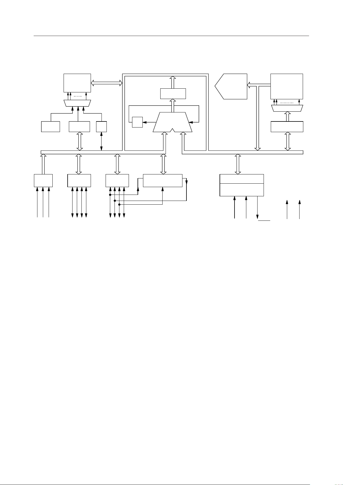
BLOCK DIAGRAM
MSM6411A¡ Semiconductor
RAM
32 ¥ 4 bits
DEC
2 0
P2
2 1 0
SP
L
3 0
P1
3 2 1 0
INT SISO
H
P0
3 2 1 0
SCK
C
I SR O
7 f 0
ACC
3 0
ALU
INST.
DEC.
RESET
INT.C
T.G
OSC
ROM
1024 ¥ 8 bits
DEC
PC
9 0
1
VDDGND
OSC
0
2/11

PIN CONFIGURATION (TOP VIEW)
MSM6411A¡ Semiconductor
P1.2
P1.3
P2.0/INT
P2.1
P2.2
OSC
OSC
GND
1
2
3
4
5
6
1
7
0
8
16
15
14
13
12
11
10
9
V
DD
P1.1
P1.0
P0.3/SI
P0.2/SO
P0.1/SCK
P0.0
RESET
16-Pin Plastic DIP
PIN DESCRIPTIONS
Pin
10
11
12
13
14
15
1
2
3
4
5
7
6
9
16
8I —
Symbol Type Description During reset
P0.0
P0.1/SCK
I/O
P0.2/SO
4-bit input-output port. P0.1 to P0.3 are used as both
input-output ports and shift register pins.
"1"
P0.3/SI
P1.0
P1.1
I/O 4-bit input-output port. "1"
P1.2
P1.3
P2.0/INT
P2.1
I
and INT input pin (falling edge trigger input).
3-bit input port with latch. P2.0 is used as both input port
Latch is reset.
("0")
P2.2
OSC
0
OSC
1
RESET I Input pin for system reset.
V
DD
GND
I System clock input pin. Clocked in
O
the oscillator circuit.
System clock output pin. This pin and OSC
pin make up
0
—
—
I Power supply voltage pin.
—
Ground pin.
3/11

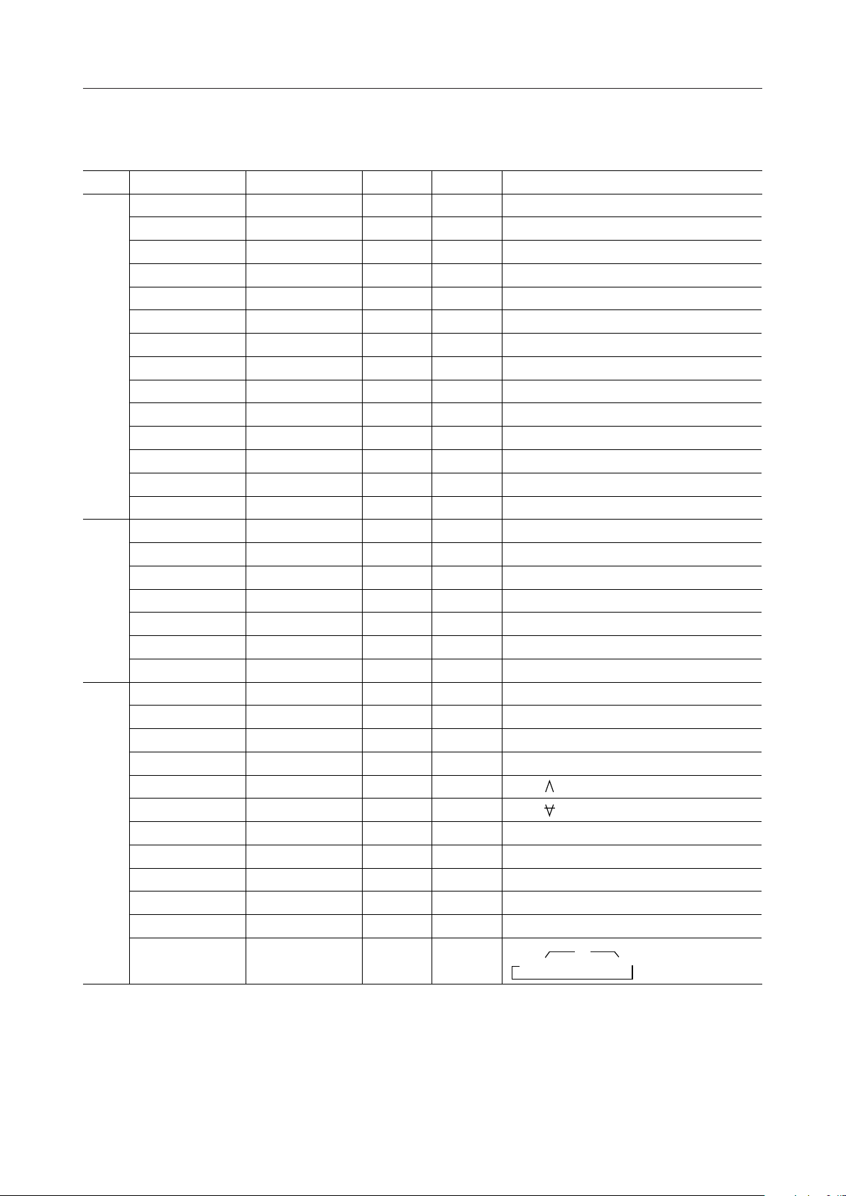
INSTRUCTION LIST
Mnemonic Byte DescriptionCode Cycle
LAI n 1 A¨n90-9F 1
LLI n 1 L¨n80-8F 1
LHLI nn 2 HL¨nn15nn 2
LAL 1 A¨L21 1
LLA 1 L¨A2D 1
LAM 1 A¨M38 1
LMA 1 M¨A2F 1
LAMD mm 2 A¨Md10mm 2
LMAD mm 2 Md¨A11mm 2
LMSR 2 M(w)¨SR3E5A 2
Load, Push, Pop, ExchangeArithmetic Increment and Decrement
LSRM 2 SR¨M(w)3E52 2
PUSH 1 ST¨C, A, H, L, SP¨SP – 11C 3
POP 1 C, A, H, L¨ST, SP¨SP + 11D 3
X1A¨M28 1
INL 1 L¨L + 1, SKIP IF L = "0"31 1
INH 1 H¨H + 1, SKIP IF H = "0"32 1
INM 1 M¨M + 1, SKIP IF M = "0"33 1
INMD mm 2 Md¨Md – 1, SKIP IF Md = "0"12mm 2
DCL 1 L¨L – 1, SKIP IF L = "F"35 1
DCH 1 H¨H – 136 1
DCM 1 M¨M – 1, SKIP IF M = "F"37 1
ADS 1 A¨A + M, SKIP IF Cy = "1"02 1
ADC 1 C, A¨C + A + M03 1
AIS n 2 A¨A + n, SKIP IF Cy = "1"3E4n 2
DAS 1 A¨A + 100A 1
AND 1 A¨A M0D 1
EOR 1 A¨A M04 1
CMA 1 A¨A0B 1
CAM 1 SKIP IF A = M16 1
SC 1 C¨"1"07 1
RC 1 C¨"0"08 1
TC 1 SKIP IF C = "1"09 1
RAL 10E 1
MSM6411A¡ Semiconductor
A
C¨3¨2¨1¨0¨
4/11
 Loading...