OKI MSM534001E Datasheet

Semiconductor
MSM534001E
524,288-Word x 8-Bit MASKROM
DESCRIPTION
The OKI MSM534001E is a high-speed silicon gate CMOS Mask ROM with 524,288-word
x 8-bit capacity. The MSM534001E operates on a single 5.0V power supply and is TTL
compatible. The chip's asynchronous I/O requires no external clock assuring easy operation.
A power-down mode provides low power dissipation when the chip is not selected. The CE
and OE pins are provided as control signals that permit three-stated output allowing easy
memory expansion on a system bus. The MSM534001E is suited for use as large capacity
fixed memory for microcomputers and data terminals.
FEATURES
Single 5.0V power supply
524,288-words x 8-bit
Access time
80ns MAX
Input/Output TTL compatible
Tri-State output configurations
Internal powerdown function
Packages:
32-PIN PLASTIC DIP (DIP32-P-600-2.54)
32-PIN PLASTIC SOP (SOP32-P-525-1.27-K)
32-PIN PLASTIC TSOP (TSOP32-P-814-0.50-K)
4MEPROM (32-PIN) pin compatible
1

MSM534001E
BLOCK DIAGRAM
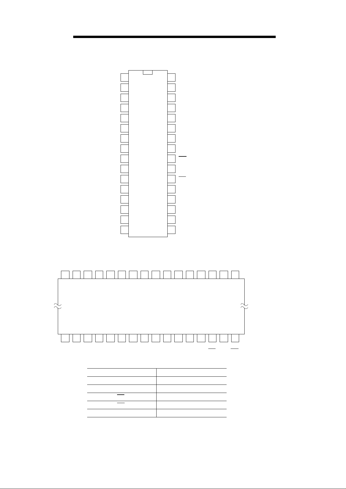
NC
A16
A15
A12
A7
A6
A5
A4
A3
A2
A1
A0
D0
D1
D2
V
SS
1
2
3
4
5
6
7
8
9
10
11
12
13
14
15
16
32PIN DIP,SOP
32
31
30
29
28
27
26
25
24
23
22
21
20
19
18
17
V
CC
A18
A17
A14
A13
A8
A9
A11
OE
A10
CE
D7
D6
D5
D4
D3
A5 A7 A15 NC A8 A11
A4 A6 A12 A16 V
CC
A14A18
A17 A13 A9
16 15 14 13 12 11 10 9 8 7 6 5 4 3 2 1
TSOP TOP VIEW
17 18 19 20 21 22 23 24 25 26 27 28 29 30 31 32
A3 A1 D0 D2 D3 D5 D7 A10
A2 A0 D1 V
SS
D6 CE OED4
Pin Name Function
A0 to A18 Address input
D0 to D7
CE
OE
V
, V
CC
SS
Data output
Chip enable
Output enable
Power supply
2

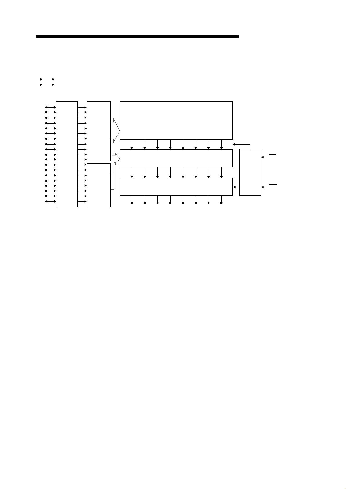
BLOCK DIAGRAM
VCCV
SS
MSM534001E
A0
A1
A2
A3
A4
A5
A6
A7
A8
A9
A10
A11
A12
A13
A14
A15
A16
A17
A18
Address
Buffer
X
Decoder
Y
Decoder
Memory Cell
Matrix
524,288 x 8
Multiplexer
Output Buffer
D0
D1 D2 D3 D4 D5 D6
D7
CE
OE
Control
CE
OE
3
 Loading...