

OKI MSM514400E-60SJ, MSM514400E-60TS-K, MSM514400E-70SJ, MSM514400E-70TS-K Datasheet
Semiconductor
This version : Sep.2000
MSM514400E
1,048,576-Word x 4-Bit DYNAMIC RAM : FAST PAGE MODE TYPE
DESCRIPTION
The MSM514400E is a 1,048,576-word × 4-bit dynamic RAM fabricated in Oki’s silicon-gate CMOS
technology. The MSM514400E achieves high integration, high-speed operation, and low-power consumption
because Oki manufactures the device in a quadruple-layer polysilicon/double-layer metal CMOS process. The
MSM514400E is available in a 26/20-pin plastic SOJ, 26/20-pin plastic TSOP.
FEATURES
• 1,048,576-word × 4-bit configuration
• Single 5V power supply, ± 10% tolerance
• Input : TTL compatible, low input capacitance
• Output : TTL compatible, 3-state
• Refresh : 1024 cycles/16 ms
• Fast page mode, read modify write capability
• CAS before RAS refresh, hidden refresh, RAS-only refresh capability
• Multi-bit test mode capability
• Package options:
26/20-pin 300mil plastic SOJ (SOJ26/20-P-300-1.27) (Product : MSM514400E-xxSJ)
26/20-pin 300mil plastic TSOP (TSOPII26/20-P-300-1.27-K) (Product : MSM514400E-xxTS-K)
xx indicates speed rank.
PRODUCT FAMILY
Family
MSM514400E-60 60ns 30ns 15ns 15ns 110ns 468mW
MSM514400E-70 70ns 35ns 20ns 20ns 130ns 413mW
Access Time (Max.) Power Dissipation
t
RAC
t
AA
t
CAC
t
OEA
Cycle Time
(Min.)
Operating (Max.) Standby (Max.)
5.5mW
1/14
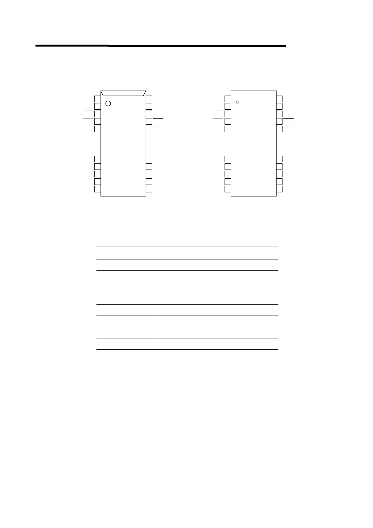
PIN CONFIGRATION (TOP VIEW)
MSM514400E
DQ1 V
DQ2
WE
RAS
A9
A0
A1
A2
A3
V
1
2
3
4
5
9
10
11
12
13
CC
26
25
24
23
22
18
17
16
15
14
26/20-Pin Plastic SOJ
Pin Name Function
A0–A9 Address Input
RAS
SS
DQ4
DQ3
CAS
OE
A8
A7
A6
A5
A4
DQ1 V
1
DQ2
2
WE
3
RAS
4
A9
5
9
A0
10
A1
11
A2
12
A3
13
V
CC
26/20-Pin Plastic TSOP
Row Address Strobe
(K Type)
26
25
24
23
22
18
17
16
15
14
SS
DQ4
DQ3
CAS
OE
A8
A7
A6
A5
A4
CAS
Column Address Strobe
DQ1–DQ4 Data Input/Data Output
OE
WE
V
CC
V
SS
Output Enable
Write Enable
Power Supply (5 V)
Ground (0 V)
Note : The same power supply voltage must be provided to every VCC pin, and the
same GND voltage level must be provided to every V
SS
pin.
2/14
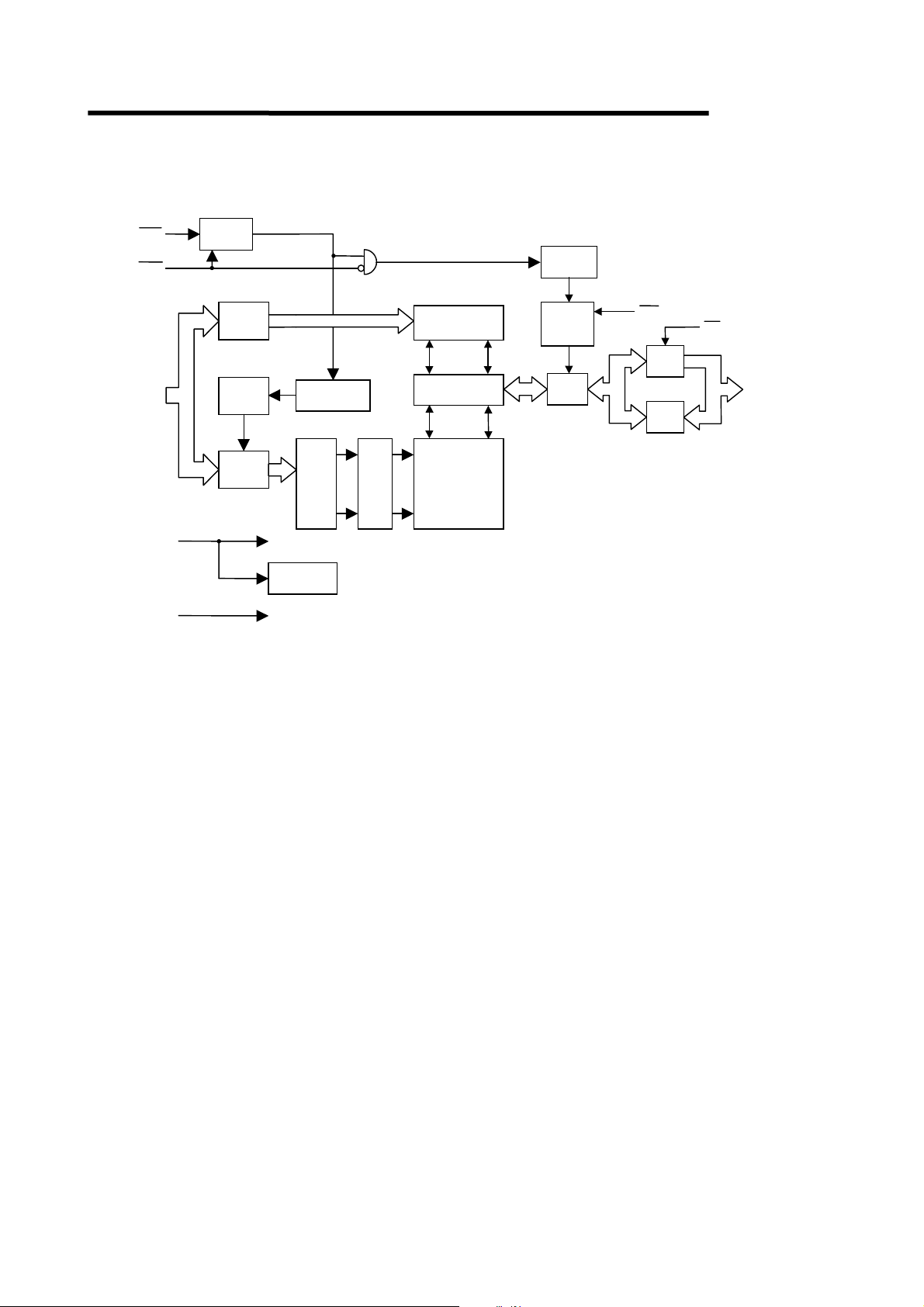
BLOCK DIAGRAM
A0-A9
DQ1-DQ4
OEWERAS
CAS
VCCV
Timing
Generator
MSM514400E
Timing
Generator
Column
10
Address
Buffers
Internal
Address
Counter
Row
Address
Buffers
SS
1010
On Chip
V
Generator
BB
Refresh
Control Clock
Row
De-
coders
Word
Drivers
10
Column
decoders
Sense Amplifiers
Memory
Cells
4
Write
Clock
Generator
I/O
Selector
Output
4
Buffers
4
4
Buffers
Input
4
4
4
3/14
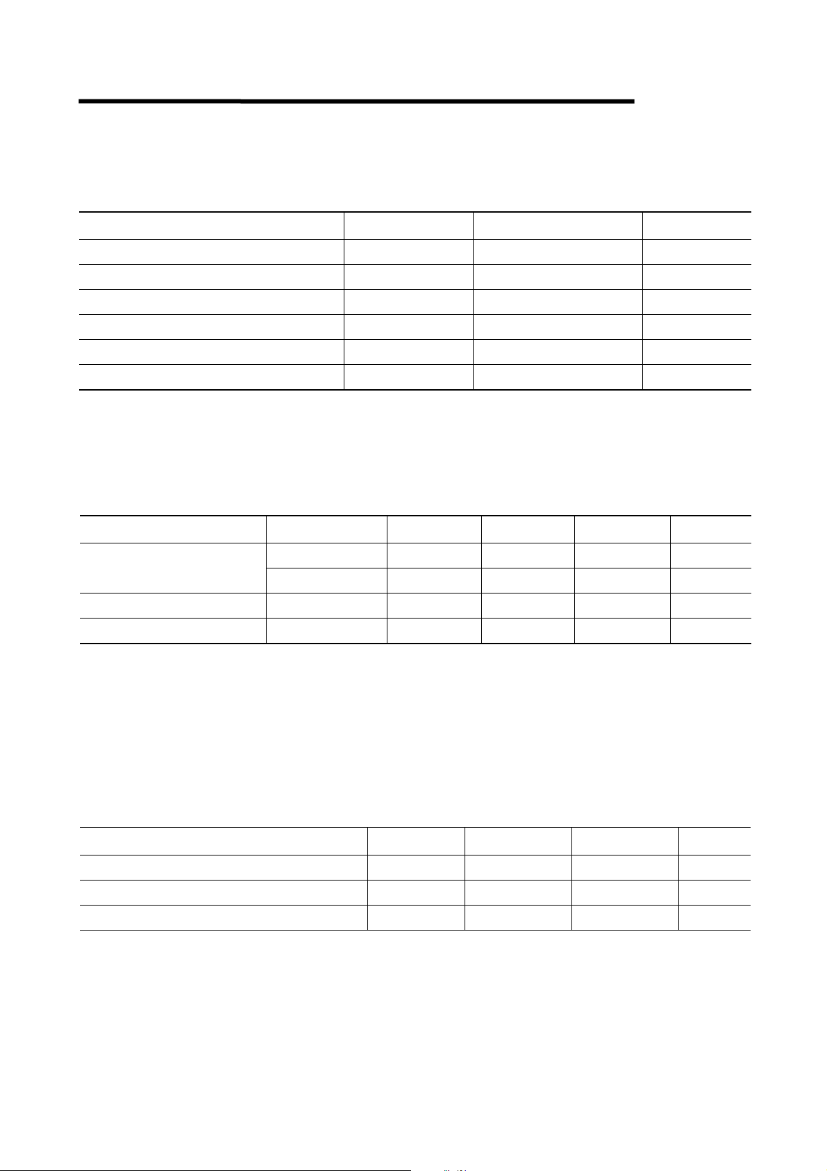
ELECTRICAL CHARACTERI S TICS
Absolute Maximum Ratings
Parameter Symbol Rating Unit
MSM514400E
Voltage on Any Pin Relative to V
Voltage on VSS Supply Relative to V
SS
SS
Short Circuit Output Current I
Power Dissipation P
Operating Temperature T
Storage Temperature T
VIN, V
V
OS
CC
D*
opr
stg
*: Ta = 25°C
Recommended Operating Conditions
Parameter Symbol Min. Typ. Max. Unit
V
Power Supply Voltage
Input High Voltage
Input Low Voltage
V
V
V
CC
SS
IH
IL
OUT
−
0.5 to Vcc + 0.5
−
0.5 to 7.0
V
V
50 mA
1W
0 to 70 °C
−
55 to 150
°C
(Ta = 0 °C to 70 °C)
4.5 5.0 5.5 V
000V
*1
0.8 V
V
−
2.4
0.5
*2
Vcc + 0.5
Notes: *1. The input voltage is VCC + 2.0V when the pulse width is less than 20ns (the pulse width is with
respect to the point at which V
*2. The input voltage is V
the point at which V
− 2.0V when the pulse width is less than 20ns (the pulse width respect to
SS
is applied).
SS
is applied).
CC
Capacitance
(Vcc = 5V ± 10%, Ta = 25°C, f=1MHz)
Parameter Symbol Typ. Max. Unit
Input Capacitance (A0 – A9)
Input Capacitance (
RAS, CAS, WE, OE
Output Capacitance (DQ1 – DQ4)
C
IN1
)
C
C
IN2
I/O
6pF
7pF
7pF
4/14
DC Characteristics
MSM514400E
(Vcc = 5V ± 10%, Ta = 0°C to 70°C)
Parameter Symbol Condition
Output High Voltage
Output Low Voltage
Input Leakage Current
Output Leakage Current
Average Power Supply
Current
(Operating)
Power Supply Current
(Standby)
Average Power Supply
Current
RAS
(
-only Refresh)
Power Supply Current
(Standby)
V
V
I
I
LO
I
CC1
I
CC2
I
CC3
I
CC5
OH
OL
LI
IOH = −5.0mA
IOL = 4.2mA
≤
I
6.5V;
0V ≤ V
All other pins not
under test = 0V
DQ disable
0V ≤ V
RAS, CAS
t
RC
RAS, CAS
≤ 5.5V
O
= Min.
cycling,
= V
IH
RAS, CAS
≥
V
−0.2V
CC
RAS
cycling,
CAS
= V
,
IH
= Min.
t
RC
RAS
= V
,
IH
CAS
= V
,
IL
DQ = enable
MSM514400
E-60
MSM514400
E-70
Unit Note
Min. Max. Min. Max.
2.4
V
CC
2.4
V
CC
V
00.400.4V
−
10
−
10
10
10
85
2
−
10
−
10
10
10
µ
A
µ
A
75 mA 1, 2
2
mA 1
1
85
5
1
75 mA 1, 2
5mA1
Average Power Supply
Current
(CAS before
RAS
Refresh)
Average Power Supply
Current
(Fast Page Mode)
I
CC6
I
CC7
RAS
CAS
RAS
CAS
t
PC
= Min.
= cycling,
before
= V
RAS
,
IL
cycling,
Notes: 1. ICC Max. is specified as ICC for output open condition.
2. The address can be changed once or less while RAS = V
3. The address can be changed once or less while CAS = V
85
70
.
IL
.
IH
75 mA 1, 2
60 mA 1, 3
5/14
 Loading...