

Page 1

E2N0026-18-Y3
Preliminary
This version: Nov. 1998
ML60851A¡ Semiconductor
¡ Semiconductor
ML60851A
USB Device Controller
GENERAL DESCRIPTION
The ML60851A is a general purpose Universal Serial Bus (USB) device controller. The ML60851A
provides a USB interface, control/status block, application interface, and FIFOs. The FIFO interface
and two types of transfer have been optimized for BulkOut devices such as printers and BulkIn
devices such as digital still cameras and image scanners. In addition, Mass Storage devices are
also applicable to this device.
FEATURES
• USB 1.0 compliant
• Built-in USB transceiver circuit
• Full-speed (12 Mb/sec) support
• Supports printer device class, image device class, and Mass Storage device class
• Supports three types of transfer; control transfer, bulk transfer, and interrupt transfer
• Built-in FIFOs for control transfer
Two 8-byte FIFOs (one for receive FIFO and the other for transmit FIFO)
• Built-in FIFOs for bulk transfer (available for either receive FIFO or transmit FIFO)
One 64-byte FIFO
Two 64-byte FIFOs
• Built-in FIFO for interrupt transfer
One 8-byte FIFO
• Supports one control endpoint, two bulk endpoint addresses, and one interrupt endpoint
address
• Two 64-byte FIFOs enable fast BulkOut transfer and BulkIn transfer
• Supports 8 bit/16 bit DMA transfer
•VCC is 3.0 V to 3.6 V
• Supporting dual power supply enables 5 V application interface
• Built-in 48 MHz oscillator circuit
• Package options:
44-pin plastic QFP (QFP44-P-910-0.80-2K) (Product name: ML60851AGA)
44-pin plastic TQFP (TQFP44-P-1010-0.80-K) (Product name: ML60851ATB)
1/44
Page 2

ML60851A
BLOCK DIAGRAM
48 MHz
USB Bus
XIN
XOUT
D+
D–
Oscillator
USB
Transceiver
DPLL
Protocol
Engine
Status/Control
Endpoint FIFO/
8-byte Setup Register
Application
Interface
A7:A0
D15:D0
CS, WR, RD
RESET
INTR
DREQ
DACK
Application
Module
(Local MCU)
ML60851A¡ Semiconductor
2/44
Page 3

PIN CONFIGURATION (TOP VIEW)
ML60851A¡ Semiconductor
V
CC3
TEST1
TEST2
XIN
XOUT
RD
WR
RESET
D+
D–
CS
CC5
AD3
AD2
AD1
AD0
444342
1
2
3
4
5
6
7
8
9
10
11
121314
INTR
D15
D14
41
15
D13
40
16
D12
AD5
AD4
VSSV
39
38
37
17
18
19
SS
CC5
V
D11
V
AD6
36
20
D10
AD7
35
21
D9
DREQ
34
22
D8
33
DACK
32
A0
31
A1
30
A2
29
A3
28
A4
27
A5
26
A6
25
A7
24
ADSEL
23
ALE
44-Pin Plastic QFP
D+
D–
V
CC3
TEST1
TEST2
XIN
XOUT
CS
RD
WR
RESET
CC5
AD3
AD2
AD1
AD0
44
43
42
41
40
1
2
3
4
5
6
7
8
9
10
11
12
13
14
15
16
D15
D14
D13
INTR
D12
AD5
AD4
VSSV
39
38
37
17
18
19
SS
CC5
V
D11
V
AD6
36
20
D10
AD7
35
21
D9
DREQ
34
22
D8
33
DACK
32
A0
31
A1
30
A2
29
A3
28
A4
27
A5
26
A6
25
A7
24
ADSEL
23
ALE
44-Pin Plastic TQFP
3/44
Page 4

PIN DESCRIPTION
ML60851A¡ Semiconductor
Pin
1, 2
6, 7
4, 5 I Test Pins (normally "L")TEST1, 2
13 to 16,
19 to 22
35 to 38,
41 to 44
25 to 32
8
9
10
12
34
33
23
24
11
Symbol Type
D+, D– USB data
XIN, XOUT
D15:D8
AD7:AD0
A7:A0
DREQ
DACK
ADSEL
RESET
CS
RD
WR
INTR
ALE
I/O
—
I/O
I/O
O
O
Description
Pin for external crystal oscillator
Data bus (MSB)
Data bus (LSB)/address input
I
Address input
I
Chip select signal input pin. LOW active
I
Read signal input pin. LOW active
I
Write signal input pin. LOW active
Interrupt request signal output pin
DMA request output pin
I
DMA acknowledge signal input pin
I
Address latch enable signal input pin
I
Address input mode select input pin. "H": address/data multiplex
I
System Reset signal input pin. LOW active
4/44
Page 5

INTERNAL REGISTERS
Addresses and Names of Registers
Address
A5:A0
00h
01h
02h
03h
04h
08h
09h
0Ah
0Bh
0Eh
0Fh
10h
11h
12h
13h
14h
15h
16h
17h
1Ah
1Bh
1Ch
1Dh
1Eh
1Fh
20h
21h
22h
23h
24h
25h
26h
27h
Read
A7, A6
11b
11b
11b
11b
11b
11b
11b
11b
11b
—
—
11b
11b
11b
11b
11b
11b
11b
11b
11b
11b
11b
11b
11b
—
11b
11b
11b
—
11b
11b
11b
—
Write
A7, A6
01b
01b
—
—
—
01b
—
—
—
01b
01b
—
—
—
—
—
—
—
—
01b
01b
—
01b
01b
—
—
—
01b
—
01b
01b
01b
—
Device Address Register
Device State Register
Packet Error Register
Receive FIFO Register
Transmit FIFO Register
Endpoint Packet-Ready Register
Endpoint 0 Receive-Byte Count Register
Endpoint 1 Receive-Byte Count Register
Endpoint 2 Receive-Byte Count Register
Flash Transmit FIFO
System Control
bmRequestType Setup Register
bRequest Setup Register
wValue LSB Setup Register
wValue MSB Setup Register
wIndex LSB Setup Register
wIndex MSB Setup Register
wLength LSB Setup Register
wLength MSB Setup Register
Assertion Select Register
Interrupt Enable Register
Interrupt Status Register
DMA Control Register
DMA Interval Register
Reserved
Endpoint 0 Receive Control Register
Endpoint 0 Receive General Register
Endpoint 0 Receive Payload Register
Reserved
Endpoint 1 Control Register
Endpoint 1 General Register
Endpoint 1 Payload Register
Reserved
ML60851A¡ Semiconductor
Register name
5/44
Page 6

Addresses and Names of Registers (Continued)
Address
A5:A0
30h
31h
32h
33h
34h
35h
36h
37h
00h
01h
02h
00h
01h
03h
Read
A7, A6
11b
11b
11b
11b
11b
11b
11b
—
01b
01b
01b
—
—
—
Write
A7, A6
—
—
01b
01b
01b
01b
01b
—
—
—
—
11b
11b
11b
Endpoint 0 Transmit Control Register
Endpoint 0 Transmit General Register
Endpoint 0 Transmit Payload Register
Endpoint 0 General Register
Endpoint 2 Control Register
Endpoint 2 General Register
Endpoint 2 Payload Register
Reserved
Endpoint 3 Control Register01b11b38h
Endpoint 3 General Register01b11b39h
Endpoint 3 Payload Register01b11b3Ah
Endpoint 0 Receive FIFO data
Endpoint 1 Receive FIFO data
Endpoint 2 Receive FIFO data
Endpoint 0 Transmit FIFO data
Endpoint 1 Transmit FIFO data
Endpoint 2 Transmit FIFO data11b—02h
Endpoint 3 Transmit FIFO data
ML60851A¡ Semiconductor
Register name
6/44
Page 7

Register Description
(W)
Device Address Register (C0h, 40h)
D7 D6 D5 D4 D3 D2 D1 D0
ML60851A¡ Semiconductor
RFU
Device Address (R/W)
The local MCU writes a device address, which is given by the SET_ADDRESS command form the
host computer, into this register. Thereafter, this device processes an only token packet transmitted
to the given device address.
Device State Register (C1h, 41h)
D7 D6 D5 D4 D3 D2 D1 D0
RFU
Default State (R/W)
Address State (R/W)
Configuration State (R/W)
Suspended State (R)
Remote Wakeup (R/W)
USB Bus Reset Clear
Default, Address, and Configuration States: D2, D1, and D0 are set to 0, 0, and 1 (default states) by
reset respectively. Changing the values of this register gives no influence on operation of this
device.
Suspended State: This register is asserted when the device enters the suspended state.
This register is deaserted by reset or when the device exits the suspended state by a resume signaling
from the USB bus.
Remote Wakeup: When this device signals a remote wakeup during the suspended state, this
register is asserted by a local MCU. This register is automatically deasserted when the device exits
the suspended state by a resume signaling from the USB bus.
USB Bus Reset Status Clear: Writing "1" to this bit causes the interrupt status to be cleared (the USB
bus reset interrupt status bit is "0" and the INTR pin is deasserted) while the USB bus reset interrupt
is being serviced (when D5, the USB bus reset interrupt status bit, of the interrupt status register is
"1" and the INTR pin is asserted). This bit is readable, and when read, its value will be always "0".
Packet Error Register (C2h, –)
D7 D6 D5 D4 D3 D2 D1 D0
RFU
Bit Stuff Error (R)
RFU = 0000b
Data CRC Error (R)
Address CRC Error (R)
PID Error (R)
7/44
Page 8

FIFO Status Register 1 (C3h, –)
pty (R)
pty (R)
)
D7 D6 D5 D4 D3 D2 D1 D0
RFU
RFU = 0000b
FIFO Status Register 2 (C4h, –)
D7 D6 D5 D4 D3 D2 D1 D0
RFU
RFU = 0000b
ML60851A¡ Semiconductor
Receive FIFO0 Full (R)
Receive FIFO0 Empty (R)
FIFO1 Full (R)
FIFO1 Em
Transmit FIFO0 Full (R)
Transmit FIFO0 Empty (R)
FIFO2 Full (R)
FIFO2 Empty (R)
FIFO3 Full (R)
FIFO3 Em
Endpoint Packet-Ready Register (C8h, 48h)
D7 D5 D4 D3 D2 D1 D0D6
RFU
EP0 Receive Packet Ready (R/Reset)
EP1 Receive Packet Ready (R/Reset)
EP2 Receive Packet Ready (R/Reset)
EP0 Transmit Packet Ready (R/Set)
EP1 Transmit Packet Ready (R/Set)
EP2 Transmit Packet Ready (R/Set)
EP3 Transmit Packet Ready (R/Set
Receive Packet Ready: When a valid packet arrives at an endpoint, this bit is automatically set and
the endpoint is locked. When "1" is written in this register, Receiver Packet Ready is reset and the
endpoint is unlocked. (This bit also is set to "0".)
When DMA is enabled, EP1 Receive Packet Ready is automatically reset after all the data in EP1 is
read during DMA transfer.
Transmit Packet Ready: When "1" is written in this register, the Transmit Packet Ready is set and the
packet in the corresponding endpoint is transmitted. Transmit Packet Ready is automatically reset
when the ACK handshake is returned from the host.
When DMA is enabled, EP1 Transmit Packet Ready is automatically set after the data written in EP1
reaches the maximum packet size during DMA transfer.
The value of this register remains unchanged when "0" is written in this register.
8/44
Page 9

Endpoint 0 Receive Byte Count Register (C9h, –)
y
D7 D6 D5 D4 D3 D2 D1 D0
ML60851A¡ Semiconductor
RFU
EP0 Byte Count (R)
Endpoint 1 Receive Byte Count Register (CAh, –)
D7 D6 D5 D4 D3 D2 D1 D0
RFU
EP1 Byte Count (R)
Endpoint 2 Receive Byte Count Register (CBh, –)
D7 D6 D5 D4 D3 D2 D1 D0
RFU
EP2 Byte Count (R)
Flash Transmit FIFO (–, 4Eh)
D7 D6 D5 D4 D2 D1 D0D3
0
000 0
In case EP1 is set as a transmission endpoint, when "1" is
written in this bit, the FIFO at EP1 is cleared and Packet
Ready at EP1 is reset by the WRITE pulse.
In case EP2 is set as a transmission endpoint, when "1" is
written in this bit, the FIFO at EP2 is cleared and Packet
Ready at EP2 is reset by the WRITE pulse.
In case EP3 is set as a transmission endpoint, when "1" is
written in this bit, the FIFO at EP3 is cleared and Packet
Read
at EP3 is reset by the WRITE pulse.
Note: Please clear all FIFOs at the same time, otherwise some of them may not be cleared.
System Control (–, 4Fh)
D7 D6 D5 D4 D2 D1 D0D3
00
0
When "1" is written in this bit, the ML60851A is reset
by the WRITE pulse.
Oscillation Stop Command
Oscillation Stop Command: Writing 1010b to D7 to D4, (writing A0h into this register) causes the
oscillator circuit of the ML60851A to be deactivated and go into the standby mode.
When oscillation is stopped, reading and writing into the register is possible but reading and writing
into FIFO is not possible. Asserting the RESET pin restarts oscillation.
9/44
Page 10

bmRequestType Setup Register (D0h, –)
D7 D6 D5 D4 D2 D1 D0D3
ML60851A¡ Semiconductor
Type (R)
Data Transfer Direction (R)
Recipient (R)
bRequest Setup Register (D1h, –)
D7 D6 D5 D4 D2 D1 D0D3
Specific Request (R)
• wValueLSB Setup Register (D2h, –)
D7:D0 = LSB of Word Size Field (R)
• wValueMSB Setup Register (D3h, –)
D7:D0 = MSB of Word Size Field (R)
0 = Device
1 = Interface
2 = Endpoint
3 = Others
4 to 31 = Reserved
0 = Standard
1 = Class
2 = Vendor
3 = Reserved
0 = Host to device
1 = Device to host
• wIndexLSB Setup Register (D4h, –)
D7:D0 = LSB of Word Size Field (R)
• wIndexMSB Setup Register (D5h, –)
D7:D0 = MSB of Word Size Field (R)
• wLengthLSB Setup Register (D6h, –)
This field defines the length of data that is transferred in the second stage (data stage) of control
transfer. (R)
• wLengthMSB Setup Register (D7h, –)
This field defines the length of data that is transferred in the data stage of control transfer. (R)
10/44
Page 11

Assertion Select Register (DAh, 5Ah) (R/W)
D7 D6 D5 D4 D3 D2 D1 D0
RFU
Assertion
of DACK
Assertion
of DREQ
Interrupt Enable Register (DBh, 5Bh) (R/W)
D7 D6 D5 D4 D3 D2 D1 D0
Assertion
of INTR
0 = Active LOW (Initial value)
1 = Active HIGH
0 = Active LOW (Initial value)
1 = Active HIGH
0 = Active HIGH (Initial value)
1 = Active LOW
Setup Ready
Interrupt Enable
EP1 Packet Ready
Interrupt Enable
EP2 Packet Ready
Interrupt Enable
EP0 Receive Packet Ready
Interrupt Enable
EP0 Transmit Packet Ready
Interrupt Enable
USB Bus Reset
Interrupt Enable
Suspended State
Interrupt Enable
EP3 Packet Ready
Interrupt Enable
ML60851A¡ Semiconductor
Initial value of D0 is 1.
Initial values of D1 to D7 are 0.
11/44
Page 12

ML60851A¡ Semiconductor
p
Interrupt Status Register (DCh, 5Ch) (R)
D7 D6 D5 D4 D3 D2 D1 D0
Setup Ready
Interrupt Status (R)
EP1 Packet Ready
Interrupt Status (R)
EP2 Packet Ready
Interrupt Status (R)
EP0 Receive Packet Ready
Interrupt Status (R)
EP0 Transmit Packet Ready
Interrupt Status (R)
USB Bus Reset
Interrupt Status
Suspended State
Interrupt Status (R)
EP3 Packet Ready
Interru
t Status
Setup Ready Interrupt Status: Equivalent to Setup Ready at (F3h) described later when the corresponding
Interrupt Enable bit is asserted.
EP1 Packet Ready Interrupt Status: Equivalent to EP1 Receive Packet Ready (the complement of EP1
Transmit Packet Ready when EP1 is set for transmitter) at (C8h) described before when the
corresponding Interrupt Enable bit is asserted.
EP2 Packet Ready Interrupt Status: Equivalent to EP2 Receive Packet Ready (the complement of EP2
Transmit Packet Ready when EP2 is set for transmitter) at (C8h) described before when the
corresponding Interrupt Enable bit is asserted.
EP0 Receive Packet Ready Interrupt Status: Equivalent to EP0 Receive Packet Ready at (C8h) described
before when the corresponding Interrupt Enable bit is asserted.
EP0 Transmit Packet Ready Interrupt Status: Equivalent to the complement of EP0 Transmit Packet
Ready at (C8h) described before when the corresponding Interrupt Enable bit is asserted.
USB Bus Reset Interrupt Status: This bit is set to "1" at USB bus reset when the D5 bit of the interrupt
enable register (DBh) is "1". To return this bit back to "0", "1" should be written to the D5 bit of the
device states register.
Suspended State Interrupt Status: Equivalent to Suspended State Register at (C1h) described before
when the corresponding Interrupt Enable bit is asserted.
EP3 Packet Ready Interrupt Status: When the D7 bit of the interrupt enable register (DBh) is "1", the
complement of the D7 bit of the endpoint packet ready register (C8h) is being copied.
12/44
Page 13

ML60851A¡ Semiconductor
DMA Control Register (DDh, 5Dh) (R/W)
D7 D6 D5 D4 D3 D2 D1 D0
RFU
Transfer
Mode
Transfer
Size
Byte
Count
Address
Mode
DMA
Enable
0 = Disables DMA Transfer (Initial value)
1 = Enables DMA Transfer for EP1
0 = Single Address Mode (Initial value)
1 = Dual Address Mode
0 = (Initial value)
1 = Inserts EP1 receive byte count into the top byte or
top word of the transfer data. (Note 1)
0 = Byte (8 bits) (Initial value)
1 = Word (16 bits) (Note 2)
0 = Single Transfer Mode (Initial value)
1 = Demand Transfer Mode
(Note 1) When 16-bit mode is set, the upper byte of the top word is 00h.
(Note 2) When 16-bit mode is set and the packet size is an odd-number byte, the upper byte of the
last word is 00h.
DMA Interval Register (DEh, 5Eh) (R/W)
D7 D6 D5 D4 D3 D2 D1 D0
This register specifies a DMA transfer interval between de-assertion and re-assertion of DREQ in
Single Transfer mode. The interval is specified between 0 and 255 (bit times). The initial value is 0.
1-bit time = 1/12 MHz (= 84 ns)
13/44
Page 14

Endpoint 0 Receive Control Register (E0h, –)
(R)
D7 D6 D5 D4 D3 D2 D1 D0
ML60851A¡ Semiconductor
RFU
00000RFU
Configuration Bit (R)
Transfer Type (R)
Endpoint Address
Configuration Bit: Only when this bit is asserted ("1"), a packet transmitted from a host computer
to this EP is received. The packet is ignored when this bit is deasserted ("0").
This bit is deasserted by system reset and is asserted by USB reset (both D+ and D- are 0s for more
than 2.5 ms).
Endpoint 0 Receive General Register (E1h, –)
D7 D6 D5 D4 D3 D2 D1 D0
RFU
Data Sequence
Toggle Bit (R)
Endpoint 0 Receive Payload Register (E2h, 62h)
D7 D6 D5 D4 D3 D2 D1 D0
RFU
Maximum Packet Size (R/W)
14/44
Page 15

ML60851A¡ Semiconductor
(
)
Endpoint 1 Control Register (E4h, 64h)
Register to set the attribute of EP1.
To use EP1, the local MCU writes EP1's attribute in this register by the request from the host
computer.
D7 D6 D5 D4 D3 D2 D1 D0
00110
Configuration Bit (R/W)
Stall Bit (R/W)
Transfer Type (R)
Transfer Direction (R/W)
10 = Bulk Transfer
Endpoint Address (R)
0 = Reception (OUT endpoint) (Supports printer)
1 = Transmission
IN endpoint) (Supports scanner, DSC
Configuration Bit: Only when this bit is asserted ("1"), a packet transmitted from the host computer
to this EP is received. The packet is ignored when this bit is deasserted ("0").
Whether or not this EP is configured can be known by referencing this bit.
Stall Bit: When this bit is asserted ("1"), a stall handshake for a packet transmitted from the host
computer to this EP is automatically returned to the host computer.
Endpoint 1 General Register (E5h, 65h)
D7 D6 D5 D4 D3 D2 D1 D0
RFU
Data Sequence
Toggle Bit (R/Reset)
Data Sequence Toggle Bit: When initializing EP, PID of DATA0 is specified after resetting the Data
Packet Toggle bit by writing "1" to this bit (this bit goes to "0").
Endpoint 1 Payload Register (E6h, 66h)
D7 D6 D5 D4 D3 D2 D1 D0
RFU
Maximum packet size (R/W)
15/44
Page 16

ML60851A¡ Semiconductor
Endpoint 3 Control Register (F8h, 78h)
Register to set the attribute of EP3.
To use EP3, the local MCU writes EP3's attribute in this register by the request from the host
computer.
D7 D6 D5 D4 D3 D2 D1 D0
01111
Configuration Bit (R/W)
Stall Bit (R/W)
Transfer Type (R)
Toggle Condition (R/W)
11 = Interrupt Transfer
Endpoint Address (R)
0 = Number
1 = Rate Feedback Mode
Configuration Bit: Only when this bit is asserted ("1"), a packet transmitted from the host computer
to this EP is received. The packet is ignored when this bit is deasserted ("0").
Whether or not this EP is configured can be known by referencing this bit.
Stall Bit: When this bit is asserted ("1"), a stall handshake for a packet transmitted from the host
computer to this EP is automatically returned to the host computer.
Toggle Condition Bit: When this bit is "0", DATA0 and DATA1 are toggled each time ACK is
received form the host computer by the EP3. Setting this bit to "1" causes the ML60851A to go
into the rate feedback mode, in which case DATA0 and DATA1 are toggled each time the packet
ready is asserted by the local MCU.
Endpoint 3 General Register (F9h, 79h)
D7 D6 D5 D4 D3 D2 D1 D0
RFU
Data Sequence
Toggle Bit (R/Reset)
Data Sequence Toggle Bit: When initializing EP, PID of DATA0 is specified after resetting the Data
Packet Toggle bit by writing "1" to this bit (this bit goes to "0").
Endpoint 3 Payload Register (FAh, 7Ah)
D7 D6 D5 D4 D3 D2 D1 D0
RFU
Maximum packet size (R/W)
16/44
Page 17

Endpoint 0 Transmit Control Register (F0h, –)
ype (R)
D7 D6 D5 D4 D3 D2 D1 D0
ML60851A¡ Semiconductor
RFU
0 0 RFU
Endpoint 0 Transmit General Register (F1h, –)
D7 D6 D5 D4 D3 D2 D1 D0
RFU
Endpoint 0 Transmit Payload Register (F2h, 72h)
D7 D6 D5 D4 D3 D2 D1 D0
RFU
Maximum Packet Size (R/W)
Endpoint 0 Transmit General Register (F3h, 73h)
D7 D6 D5 D4 D3 D2 D1 D0
Transfer T
Data Sequence
Toggle Bit (R)
RFU
RFU
Setup Ready (R/Reset)
Stall Bit (R/W)
EP0 Stage (R)
00 = Setup Stage
01 = Data Stage
10 = Status Stage
Setup Ready: When a valid setup packet has arrived at an 8-byte setup register, this register is
automatically set and the receive FIFO at endpoint 0 is locked. Writing "1" in this register resets Setup
Ready. When the data stage of Control Write transaction follows, Packet Ready at endpoint 0 is also
reset. Therefore, the endpoint 0 receive FIFO is unlocked and ready to receive the packets in the data
stage.
The value of this register remains unchanged when "0" is written in this register.
17/44
Page 18

Endpoint 2 Control Register (F4h, 74h)
(
)
D7 D6 D5 D4 D3 D2 D1 D0
01010
ML60851A¡ Semiconductor
Configuration Bit (R/W)
Stall Bit (R/W)
Transfer Type (R)
Transfer Direction (R/W)
10 = Bulk Transfer
Endpoint Address (R)
0 = Reception (OUT endpoint)
1 = Transmission
IN endpoint
Configuration Bit: Only when this bit is asserted ("1"), a packet transmitted from the host computer
to this EP is received. The packet is ignored when this bit is deasserted ("0").
Whether or not this EP is configured can be known by referencing this bit.
Stall Bit: When this bit is asserted ("1"), a stall handshake for a packet transmitted from the host
computer to this EP is automatically returned to the host computer.
Endpoint 2 General Register (F5h, 75h)
D7 D6 D5 D4 D3 D2 D1 D0
RFU
Data Sequence
Toggle Bit (R/Reset)
Data Sequence Toggle Bit: When initializing EP, PID of DATA0 is specified after resetting the Data
Packet Toggle bit by writing "1" to this bit (this bit goes to "0").
Endpoint 2 Payload Register (F6h, 76h)
D7 D6 D5 D4 D3 D2 D1 D0
RFU
Maximum Packet Size (R/W)
18/44
Page 19

ML60851A¡ Semiconductor
Endpoint 0 Receive FIFO Data (40h, –)
D7 D6 D5 D4 D3 D2 D1 D0
Endpoint 0 Receive FIFO Data (R)
Area to store data to be transmitted from the host computer to this device in the data stage of Control
Write transfer.
Endpoint 1 Receive FIFO Data (41h, –)
D7 D6 D5 D4 D3 D2 D1 D0
Endpoint 1 Receive FIFO Data (R)
Area to store data to be transmitted from the host computer to EP1 of this device in Bulk Out transfer.
This register is valid only when EP1 is set for the OUT endpoint.
Endpoint 2 Receive FIFO Data (42h, –)
D7 D6 D5 D4 D3 D2 D1 D0
Endpoint 2 Receive FIFO Data (R)
Area to store data to be transmitted from the host computer to EP2 of this device in Bulk Out transfer.
This register is valid only when EP2 is set for the OUT endpoint.
19/44
Page 20

ML60851A¡ Semiconductor
Endpoint 0 Transmit FIFO Data (–, C0h)
D7 D6 D5 D4 D3 D2 D1 D0
Endpoint 0 Transmit FIFO Data (W)
Area to store data to be transmitted from this device to the host computer in the data stage of Control
Read transter.
Endpoint 1 Transmit FIFO Data (–, C1h)
D7 D6 D5 D4 D3 D2 D1 D0
Endpoint 1 Transmit FIFO Data (W)
Area to store data to be transmitted from EP1 of this device to the host computer in Bulk In transfer.
This register is valid only when EP1 is set for the IN endpoint.
Endpoint 2 Transmit FIFO Data (–, C2h)
D7 D6 D5 D4 D3 D2 D1 D0
Endpoint 2 Transmit FIFO Data (W)
Area to store data to be transmitted from EP2 of this device to the host computer in Bulk In transfer.
This register is valid only when EP2 is set for the IN endpoint.
Endpoint 3 Transmit FIFO Data (–, C3h)
D7 D6 D5 D4 D3 D2 D1 D0
Endpoint 3 Transmit FIFO Data (W)
Area to store data to be transmitted from EP3 of this device to the host computer in Bulk In transfer.
This register is valid only when EP3 is set for the IN endpoint.
20/44
Page 21

ML60851A¡ Semiconductor
ABSOLUTE MAXIMUM RATINGS
Parameter Symbol Condition Rating Unit
Power Supply 3 V
Power Supply 5 V
Input Voltage V
Storage Temperature T
CC3
CC5
I
STG
— –0.3 to +4.6 V
— –0.5 to +6.5 V
— –0.3 to V
+ 0.3 V
CC5
— –55 to +150 °C
RECOMMENDED OPERATING CONDITIONS
Parameter Symbol Condition Range Unit
Power Supply 3 V
Power Supply 5 V
CC3
CC5
Operating Temperature Ta — 0 to 70 °C
Oscillation Frequency F
OSC
— 3.0 to 3.6 V
— 3.0 to 5.5 V
— 48 MHz
21/44
Page 22

ML60851A¡ Semiconductor
ELECTRICAL CHARACTERISTICS
DC Characteristics (1)
(V
= V
= 3.0 to 3.6 V, V
CC3
V
CC5
CC3
CC3
Max.
+ 0.3
+ 0.3—V
¥ 0.2—–0.3V
50
5
50
50
Typ.
—
——
——V
——
——
Parameter Condition
High-level Input
Voltage
Symbol
V
IH
Low-level Input
Voltage
IL
High-level Input
Voltage
IH
Low-level Input
Voltage
Schmitt Trigger
Input Voltage
High-level
Output Voltage
Low-level
Output Voltage
High-level Input
Current
Low-level Input
Current
3-state Output
Leakage Current
Power Supply
Current (Operating)
Power Supply
Current (Standby)
IL
t+
t–
V
OH
V
OL
IH
IL
OZH
OZL
CC3
CC5
CCS3
CCS5
I
(Vt+) – (Vt–)V—0.40.1DV
OH
I
I
OH
OL
I
V
=
OL
IH
t
V
V
OH
V
OL
Note 3 mAI
Note 3 mAI
CC5
Min.
—
2.0
—V+0.8—–0.3V
—VV
CC3
¥ 0.8V
—VV
—V2.01.6—V
–100 mAV——V
=
–4 mA V——2.4
CC5
– 0.2
= 100 mAV0.2——
= 4 mA V0.4——
= V
CC5
= V
IL
SS
= V
CC5
= V
SS
—mA——I
—mA——I
Notes: 1. Applied to D15:D8, AD7:AD0, A7:A0, CS, RD, WR, DACK, ALE, and ADSEL.
2. Applied to XIN, A7:A0, CS, RD, WR, DACK, ALE, and ADSEL. VIH = V
3. The XIN pin is fixed to High level or Low level in the suspend state. All the output
pins are open.
= 0 V, Ta = 0 to 70°C)
SS
Applicable pin
Unit
V
Note 1
XIN
RESET—V—1.20.8V
D15:D8
AD7:AD0
INTR, DREQ
mA10.01—I
Note 2
mA—–0.01–1I
mA10.01—I
mA—–0.01–1I
D15:D8
AD7:AD0
for only XIN.
CC3
V
CC3
CC5
V
CC3
V
CC5
22/44
Page 23

DC Characteristics (2)
Parameter Condition
High-level Input
Voltage
Low-level Input
Voltage
Schmitt Trigger
Input Voltage
High-level
Output Voltage
Low-level
Output Voltage
High-level Input
Current
Low-level Input
Current
3-state Output
Leakage Current
Power Supply
Current (Operating)
Power Supply
Current (Standby)
Symbol
V
IH
IL
t+
t–
t
V
OH
V
OL
IH
IL
OZH
OZL
CC3
CC5
CCS3
CCS5
(Vt+) – (Vt–)V—0.30.2DV
I
OH
I
OH
I
OL
I
OL
V
V
V
V
(V
= 4.5 to 5.5 V, V
CC5
—
—V+0.8—–0.5V
—V2.21.7—V
=
–100 mAV——V
=
–8 mA V——3.7
CC5
= 100 mAV0.2——
= 8 mA V0.4——
= V
IH
CC5
= V
IL
SS
= V
OH
CC5
= V
OL
SS
—mA——I
—mA——I
Note 3 mAI
Note 3 mAI
Min.
2.2
– 0.2
= 3.0 to 3.6 V, V
CC3
Typ.
—
——
——
——
——
V
CC5
Max.
+ 0.5
50
5
50
50
ML60851A¡ Semiconductor
= 0 V, Ta = 0 to 70°C)
SS
Applicable pin
Unit
V
Note 1
RESET—V—1.40.8V
D15:D8
AD7:AD0
INTR, DREQ
mA100.01—I
Note 2
mA—–0.01–10I
mA100.01—I
mA—–0.01–10I
D15:D8
AD7:AD0
V
CC3
V
CC5
V
CC3
V
CC5
Notes: 1. Applied to D15:D8, AD7:AD0, A7:A0, CS, RD, WR, DACK, ALE, and ADSEL. The DC
characteristics (1) applies to XIN.
2. Applied to A7:A0, CS, RD, WR, DACK, ALE, and ADSEL. The DC characteristics (1)
applies to XIN.
3. The XIN pin is fixed to High level or Low level in the suspend state. All the output
pins are open.
23/44
Page 24

DC Characteristics (3) USB Port
Parameter Condition
Differential Input
Sensitivity
Differential Common
Mode Range
Single Ended
Receiver Threshold
High-level Output
Voltage
Low-level Output
Voltage
Output Leakage
Current
Symbol
V
DI
CM
SE
OH
OL
LO
(D+) – (D–)
Includes V
RL of 15 kW to V
RL of 1.5 kW to 3.6 V V0.3V
0 V < V
ML60851A¡ Semiconductor
(V
= 3.0 to 3.6 V, V
CC3
Max.Typ.Min.
0.2
range V2.50.8V
DI
SS
< 3.3 V mA+10–10I
IN
= 0 V, Ta = 0 to 70°C)
SS
Applicable pin
Unit
V
V2.00.8V
D+, D–
V3.62.8V
AC Characteristics USB Port
Parameter
Rise Transition Time
Fall Transition Time
Rise/Fall Time
Matching
Output Signal
Crossover Voltage
Driver Output
Resistance
Data Rate
Symbol
t
R
F
RFM
CRS
DRV
DRATE
Condition
(Notes 1. and 2.)
CL = 50 pF
CL = 50 pF ns254t
(t
)
R/tF
Steady State Driver W43Z
Ava. Bit
Rate (12 Mb/s ±0.25%)
4
28
Notes: 1. 1.5 kW pull-up to 2.8 V on the D+ data line.
2. Measured from 10% to 90% of the data signal.
= 3.0 to 3.6 V, V
(V
CC3
= 0 V, Ta = 0 to 70°C)
SS
Applicable pin
Max.Typ.Min.
25
Unit
ns
%14090t
V21.2V
D+, D–
Mbs12.0311.97t
24/44
Page 25

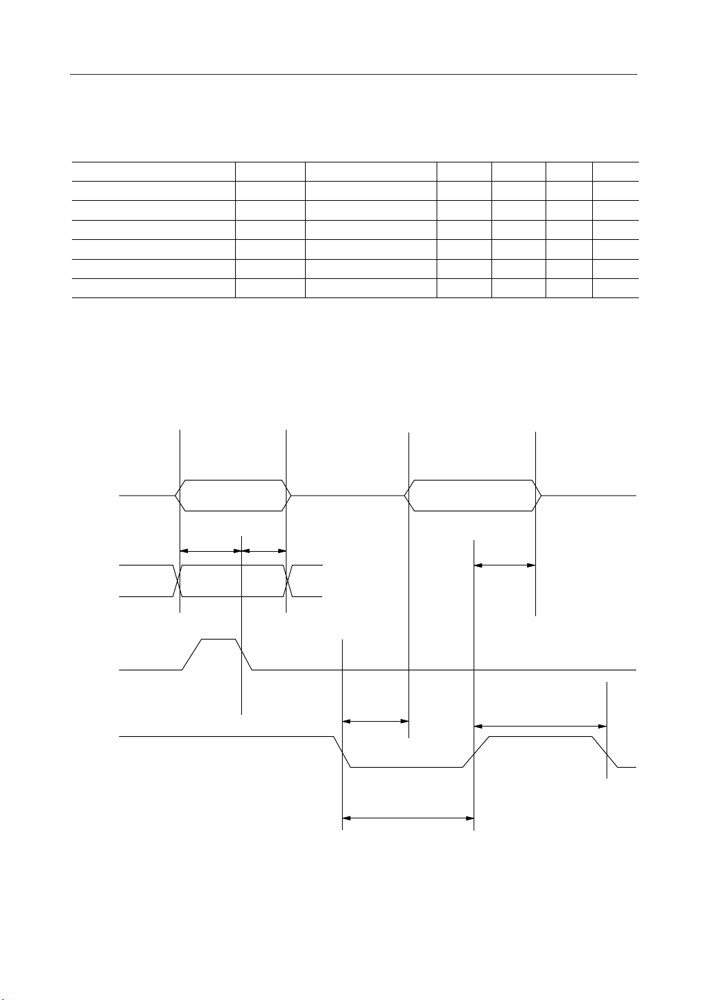
TIMING DIAGRAM
READ Timing (1)
(Address Separate ADSEL = 0)
ML60851A¡ Semiconductor
Parameter Symbol Condition Note
Address Setup Time (RD)t
Address Setup Time (CS)t
Address (CS) Hold Time t
Read Data Delay Time t
Read Data Hold Time t
Recovery Time t
FIFO Access Time t
1
1
2
3
4
5
6
(RD)
Load 20 pF
FIFO READ
FIFO READ
21 —
0
63
42
Max.Min.
—
25—
—0
—
—
Unit
ns
ns10 — 5(CS)
ns
ns
ns
ns
ns
Notes: 1. t1 and t3 are defined depending upon CS or RD which becomes active last.
2. t2 is defined depending upon CS or RD which becomes active first.
3. 3-clock time of oscillation clock (clock period: 21 ns). It is required for increment of FIFO.
4. 2-clock time of oscillation clock (clock period: 21 ns). It is required for increment of FIFO.
5. Either of them should be met.
A7:A0
5
2
1
3
4
CS
RD
AD7:AD0
t
1
t
3
t
6
t
2
t
5
t
4
DATA OUT
25/44
Page 26
READ Timing (2)
(Address/Data Multiplex ADSEL = 1)
ML60851A¡ Semiconductor
Parameter Symbol Condition Note
Address (CS) Setup Time t
Address (CS) Hold Time t
Read Data Delay Time t
Read Data Hold Time t
Recovery Time t
FIFO Access Time t
1
2
3
4
5
6
Load 20 pF
FIFO READ
FIFO READ
10 —
0
63
42
Max.Min.
—
25—
—0
—
—
Unit
ns
ns
ns
ns
ns
ns
1
2
Notes: 1. 3-clock time of oscillation clock (clock period: 21 ns). It is required for increment of FIFO.
2. 2-clock time of oscillation clock (clock period: 21 ns). It is required for increment of FIFO.
AD7:AD0
CS
t
1
t
2
DATA OUTADDRESS
t
4
ALE
RD
t
3
t
6
t
5
26/44
Page 27

WRITE Timing (1)
(Address Separate ADSEL = 0)
ML60851A¡ Semiconductor
Parameter Symbol Condition Note
Address Setup Time (WR)t
Address Setup Time (CS)t
Address (CS) Hold Time t
CS Setup Time t
Write Data Setup Time t
Write Data Hold Time t
Recovery Time t
FIFO Access Time t
1
1
2
3
4
5
6
7
FIFO WRITE
FIFO WRITE
21 —
0
63
42
Max.Min.
—
—30
—5
—
—
Notes: 1. t1 is defined depending upon CS or WR which becomes active last.
2. 3-clock time of oscillation clock (clock period: 21 ns). It is required for increment of FIFO.
3. 2-clock time of oscillation clock (clock period: 21 ns). It is required for increment of FIFO.
4. Either of them should be met.
A7:A0
t
CS
1
t
7
t
2
Unit
ns
ns10 — 4(CS)
ns
ns10 —
ns
ns
ns
ns
4(WR)
2
3
WR
AD7:AD0
t
3
t
4
DATA IN
t
6
t
5
27/44
Page 28

WRITE Timing (2)
(Address/Data Multiplex ADSEL = 1)
ML60851A¡ Semiconductor
Parameter Symbol Condition Note
Address (CS) Setup Time t
Address (CS) Hold Time t
Write Data Setup Time t
Write Data Hold Time t
Recovery Time t
FIFO Access Time t
1
2
3
4
5
6
FIFO WRITE
FIFO WRITE
10 —
0
63
42
Max.Min.
—
—30
—5
—
—
Unit
ns
ns
ns
ns
ns
ns
1
2
Notes: 1. 3-clock time of oscillation clock (clock period: 21 ns). It is required for increment of FIFO.
2. 2-clock time of oscillation clock (clock period: 21 ns). It is required for increment of FIFO.
AD7:AD0 ADDRESS DATA IN
t
1
t
2
t
4
CS
ALE
WR
t
3
t
5
t
6
28/44
Page 29

DMA Transfer Timing (1)
ML60851A to Memory (Single Transfer, Single Address Mode)
ML60851A¡ Semiconductor
Parameter Symbol Condition Note
DREQ Disable Time t
DREQ Enable Time t
DACK Hold Time t
Read Data Delay Time t
Data Hold Time t
Recovery Time t
1
2
3
4
5
Load 20 pF
Load 20 pF
8-bit DMA
6
16-bit DMA
—20
—
0
105
Notes: 1. When in Single Address mode, CS and A7:A0 are ignored.
t4 is defined depending on DACK or RD which becomes active last.
2. 3-clock time of oscillation clock (clock period: 21 ns).
3. 5-clock time of oscillation clock (clock period: 21 ns).
DREQ
DACK
t
1
t
4
t
3
Max.Min.
Unit
ns
63
—0
25—
—
ns
ns
ns
ns
1
2ns—63
—3
ns
t
2
t
6
RD
DOUT
t
5
29/44
Page 30

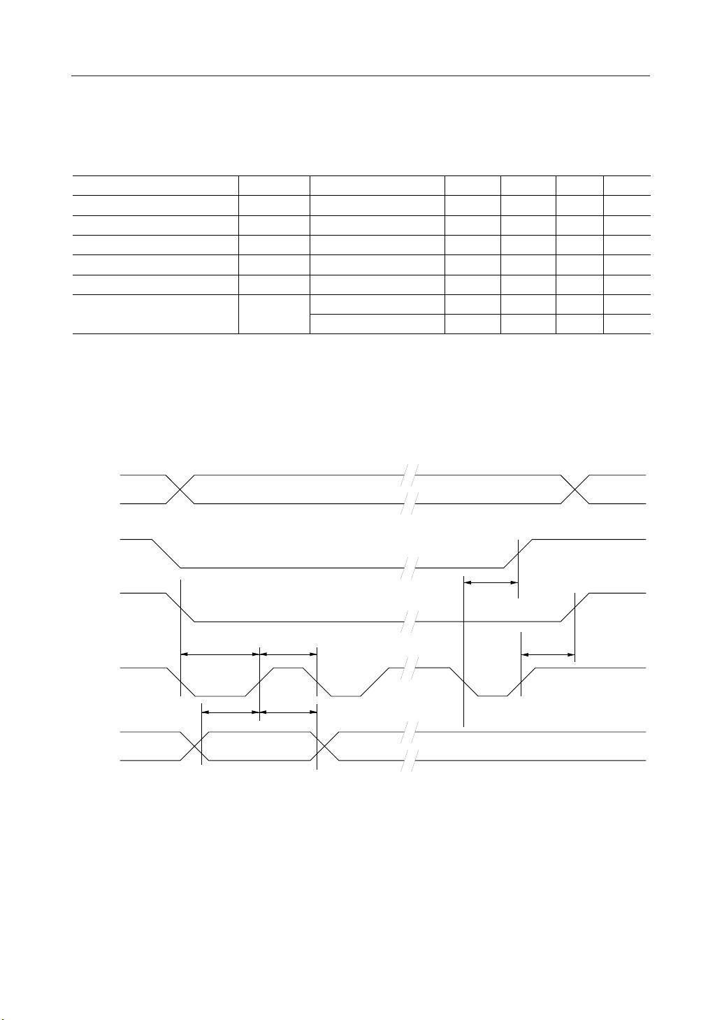
DMA Transfer Timing (2)
ML60851A to Memory (Single Transfer, Dual Address Mode)
ML60851A¡ Semiconductor
Parameter Symbol Condition Note
DREQ Disable Time t
DREQ Enable Time t
Read Data Delay Time t
Data Hold Time
Recovery Time t
1
2
3
t
4
5
Load 20 pF
Load 20 pF
8-bit DMA
16-bit DMA
Notes: 1. When in Dual Address mode, the DACK is ignored.
t3 is defined depending on CS or RD which becomes active last.
A7:A0 specifies the FIFO address.
Refer to READ Timing (1) for Address Setup Time and Address Hold Time.
2. 3-clock time of oscillation clock (clock period: 21 ns).
3. 5-clock time of oscillation clock (clock period: 21 ns).
A7:A0
DREQ
Max.Min.
—20
—
63
25—
0
—
—63
105
—3
t
2
Unit
ns
ns
ns
ns
ns
1
2ns
CS
RD
DOUT
t
1
t
t
3
t
5
4
30/44
Page 31

DMA Transfer Timing (3)
ML60851A to Memory (Demand Transfer, Single Address Mode)
ML60851A¡ Semiconductor
Parameter Symbol Condition Note
DREQ Disable Time t
DACK Hold Time t
Read Data Delay Time t
Data Hold Time
Recovery Time t
1
2
3
t
4
5
Load 20 pF
Load 20 pF
8-bit DMA
16-bit DMA
—
0—
0
105 3
Max.Min.
20
25—
—
—63
—
Unit
ns
ns
ns
ns
ns
1
2ns
Notes: 1. When in Single Address mode, t3 is defined depending on DACK or RD which becomes
active last.
A7:A0 and CS are ignored.
2. 3-clock time of oscillation clock (clock period: 21 ns).
3. 5-clock time of oscillation clock (clock period: 21 ns).
DREQ
t
1
DACK
t
5
t
2
RD
DOUT
t
3
t
4
Last Packet Read
31/44
Page 32

DMA Transfer Timing (4)
ML60851A to Memory (Demand Transfer, Dual Address Mode)
ML60851A¡ Semiconductor
Parameter Symbol Condition Note
DREQ Disable Time t
CS Hold Time t
Read Data Delay Time t
Data Hold Time
Recovery Time t
1
2
3
t
4
5
Load 20 pF
Load 20 pF
8-bit DMA
16-bit DMA
Notes: 1. When in Dual Address mode, the DACK is ignored.
t3 is defined depending on CS or RD which becomes active last.
A7:A0 specifies the FIFO address.
Refer to READ Timing (1) for Address Setup Time and Address Hold Time.
2. 3-clock time of oscillation clock (clock period: 21 ns).
3. 5-clock time of oscillation clock (clock period: 21 ns).
A7:A0
DREQ
—
0
—
0
63
105
Max.Min.
20
—
25
—
—
—3
Unit
ns
ns
ns
1
ns
2ns
ns
t1
CS
RD
DOUT
t
5
t
t
3
4
Last Packet Read
t
2
32/44
Page 33

DMA Transfer Timing (5)
Memory to ML60851A (Single Transfer, Single Address Mode)
ML60851A¡ Semiconductor
Parameter Symbol Condition Note
DREQ Disable Time t
DREQ Enable Time t
FIFO Access Time t
DACK Hold Time
Write Data Setup Time
Write Data Hold Time
Recovery Time
1
2
3
t
4
t
5
t
6
t
7
Load 20 pF
FIFO WRITE
8-bit DMA
16-bit DMA
—20
—
42
30
5
63
105
Notes: 1. When in Single Address mode, CS and A7:A0 are ignored.
2. 3-clock time of oscillation clock (clock period: 21 ns).
3. 5-clock time of oscillation clock (clock period: 21 ns).
DREQ
t
4
DACK
t
1
t
3
Max.Min.
Unit
ns
63
—1
—0
—
—
—
—
ns
ns
ns
ns
ns
ns
ns
t
2
2
3
WR
DIN
t
7
t
t
5
6
33/44
Page 34

DMA Transfer Timing (6)
Memory to ML60851A (Single Transfer, Dual Address Mode)
ML60851A¡ Semiconductor
Parameter Symbol Condition Note
DREQ Disable Time t
DREQ Enable Time t
FIFO Access Time t
Write Data Setup Time
Write Data Hold Time
Recovery Time
1
2
3
t
4
t
5
t
6
Load 20 pF
FIFO WRITE
8-bit DMA
16-bit DMA
Notes: 1. When in Dual Address mode, the DACK is ignored.
Refer to WRITE Timing (1) for Address Setup Time and Address Hold Time.
2. 3-clock time of oscillation clock (clock period: 21 ns).
3. 5-clock time of oscillation clock (clock period: 21 ns).
A7:A0
DREQ
t
1
Max.Min.
—20
—
42
30
5
63
105
63
—
—
—
—
—
t
2
Unit
ns
ns
ns
ns
ns
ns
ns
1
2
3
CS
WR
DIN
t
3
t
5
t
4
t
6
34/44
Page 35

DMA Transfer Timing (7)
Memory to ML60851A (Demand Transfer, Single Address Mode)
ML60851A¡ Semiconductor
Parameter Symbol Condition Note
DREQ Disable Time t
FIFO Access Time
DACK Hold Time
Write Data Setup Time t
Write Data Hold Time t
Recovery Time t
1
t
2
t
3
4
5
6
Load 20 pF
FIFO WRITE
8-bit DMA
16-bit DMA
—20
0
30
5
63
105
Notes: 1. When in Single Address mode, A7:A0 and CS and ignored.
2. 3-clock time of oscillation clock (clock period: 21 ns).
3. 5-clock time of oscillation clock (clock period: 21 ns).
DREQ
DACK
t
2
t
6
Max.Min.
Unit
ns
—42
—
—
—
—
—
ns
ns
ns
ns
ns
ns
1
2
3
t
1
t
3
WR
(Note)
DIN
t
4
t
5
Last Packet Write
(Note) The last Write to reach the byte size (maximum packet size) specified by the EP1 Payload
Register.
To terminate DMA transfer before reaching the maximum packet size, set EP1 Packet Ready
by writing "1" to the EP1 Transmit Packet Ready bit.
35/44
Page 36
DMA Transfer Timing (8)
(
Memory to ML60851A (Demand Transfer, Dual Address Mode)
ML60851A¡ Semiconductor
Parameter Symbol Condition Note
DREQ Disable Time t
FIFO Access Time
CS Hold Time
Write Data Setup Time t
Write Data Hold Time t
Recovery Time t
1
t
2
t
3
4
5
6
Load 20 pF
FIFO WRITE
8-bit DMA
16-bit DMA
Notes: 1. When in Dual Address mode, the DACK is ignored.
A7:A0 specifies the FIFO address.
Refer to WRITE Timing (1) for Address Setup Time and Address Hold Time.
2. 3-clock time of oscillation clock (clock period: 21 ns).
3. 5-clock time of oscillation clock (clock period: 21 ns).
A7:A0
DREQ
Max.Min.
—20
42
0
30
5
63
105
—
—
—
—
—
—
t
1
Unit
ns
ns
ns
ns
ns
ns
ns
1
2
3
CS
t
3
(Note)
WR
DIN
t
2
t
4
Note) Refer to the previous page.
t
6
t
5
Last Packet Write
36/44
Page 37

FUNCTIONAL DESCRIPTIONS
Pin Functional Description
USB Interface
ML60851A¡ Semiconductor
Signal
D+
Type
I/O
—
—I/OD–
USB data (Plus). This signal and the D– signal are the transmitted or received
data from/to USB Bus. The table below shows values and results for these signal.
D+ D– Result
0 0 Single end 0
0 1 Differential "0"
1 0 Differential "1"
1 1 Undefined
USB Data (Minus). This signal and the D+ signal are the transmitted or
received data from/to USB Bus. The table above shows values and results for
these signals.
DescriptionAssertion
Crystal Oscillator Interface
Signal
XIN For internal oscillation, connect a crystal to XIN and XOUT.
Type
I
—
—OXOUT
For external oscillation, supply an external 48 MHz clock signal to XIN.
Set XOUT to be open.
DescriptionAssertion
37/44
Page 38

Application Interface
ML60851A¡ Semiconductor
Signal
D15:D8
Type
I/O
OINTR
ODREQ
IDACK
IALE
IADSEL
IRESET
—
—I/OAD7:AD0
—IA7:A0
LOWICS
LOWIRD
LOWIWR
LOW
(Note 1)
LOW
(Note 1)
HIGH
(Note 1)
—
—
LOW
DescriptionAssertion
Upper byte (MSB) of data bus. This data bus is used by applications to access
register files and FIFO data.
Lower byte (LSB) of data bus when ADSEL is LOW.
Address and lower byte of data bus are multiplexed when ADSEL is HIGH.
Address when ADSEL is LOW. This address signal is used by application to
access register files and FIFO data.
This signal is ignored (all lows or all highs) when ADSEL is HIGH.
Chip Select. When this signal is asserted LOW, the ML60851A is selected
and ready to read or write data.
Read Strobe. When this signal is asserted LOW, the Read instruction is
executed.
Write Strobe. When this signal is asserted LOW, the Write instruction is
executed.
Interrupt Request. When this signal is asserted, the ML60851A makes an
interrupt request to the application.
DMA Request. This signal requests the Endpoint FIFO to make a DMA transfer.
DMA Acknowledge Signal. This signal, when asserted, enables accessing
FIFOs, without address bus setting.
When ADSEL is HIGH, the address and CS on AD7:AD0 is latched at the
trailing edge of this signal. This signal is ignored when ADSEL is LOW.
When ADSEL is LOW, the address is input on A7:A0 and data i input on
D15:D8 and AD7:AD0. When ADSEL is HIGH, the lower bytes (LSB) of
address and data are multiplexed on AD7:AD0.
System Reset. When this signal is asserted LOW, the ML60851A is reset.
When the ML60851A is powered on, this signal must be asserted for 1 ms.
Note: 1. Initial value immediately after resetting. Its assertion can be changed by programming.
38/44
Page 39

ML60851A¡ Semiconductor
Functional Description
The ML60851A USB device controller contains the Protocol Engine, DPLL, Timer, Status/Control,
FIFO Control, Application Interface, and Remote Wakeup blocks.
• Protocol Engine
The Protocol Engine handles the USB communication protocol. It performs control of packet
transmission/reception, generation/detection of synchronous patterns, CRC generation/checking,
NRZI data modulation, bit stuffing, and packet ID (PID) generation/checking.
• DPLL (Digital Phase Locked Loop)
The DPLL extracts clock and data from the USB differential received data (D+ and D–).
• Timer
The Timer block monitors idle time on the USB bus.
• Status/Control
The Status Control block moniors the transaction status and transmits control events to the
application through an interrupt request.
39/44
Page 40

ML60851A¡ Semiconductor
• FIFO Control
The FIFO Control block controls all FIFO operations for transmitting and receiving USB packets.
The FIFO configuration is described below.
Endpoint FIFO/8-Byte Setup Register Configuration
Endpoint Address 0
Endpoint Address 0
Endpoint Address 0
Endpoint Address 1
Endpoint Address 2
8-Byte
Setup Register
8-Byte
FIFO Rx
8-Byte
FIFO Tx
64-Byte
FIFO
64-Byte
FIFO
64-Byte
FIFO
For Control Transfer
Setup Ready
Packet Ready
Packet Ready
For Bulk Transfer
Packet Ready
DMA Request
Packet Ready
EP0 Receive FIFO
EP0 Transmit FIFO
EP1 FIFO (128 bytes)
(Selectable for transmitter
or receiver)
EP2 FIFO (64 bytes)
(Selectable for transmitter
or receiver)
Endpoint Address 3
Endpoint address Program sizeFIFO type
Reception
Transmission
Reception/Transmission
8-Byte
FIFO
Packet Ready
EP3 FIFO (8 bytes)
Function
0
0
1
8 Bytes
8 Bytes
64 Bytes (2 levels)
Transfer control
Transfer control
Bulk-In and bulk-Out
Reception/Transmission 2 64 Bytes Bulk-Out and bulk-In
Transmission
3
8 Bytes
Interrupt
Every FIFO has a flag that indicates a full or empty FIFO and the capability of re-transmitting and
re-receiving data. Endpoint addresses 1 and 2 can be used for either of reception and transmission
by writing the register.
The FIFO at endpoint address 1 can be used for DMA transfer.
40/44
Page 41

ML60851A¡ Semiconductor
• Interrupt
Interrupt factors include Packet Ready for a transmit/receive FIFO, Setup Ready for 8-byte setup
data, and Suspend. Generation of each interrupt request can be enabled or disabled by the
Interrupt Enable register.
•DMA
8-bit and 16-bit demand transfer DMA and single transfer DMA are enabled for bulk-transfer FIFO
at endpoint address 1.
In Demand Transfer mode, DREQ is asserted when a valid packet arrives at the FIFO. When the
external DMA contoller has completed transferring all byte data of a received packet, DREQ is
deasserted. Accordingly, other devices cannot access the local bus during DMA transfer.
In Single Tranfer mode, each time transfer of one byte data is completed, DREQ is deasserted.
While DREQ is deasserted, other devices can access the local bus.
• Remote Wakeup
This functional block supports the remote wakeup function.
• USB Transfers
The ML60851A supports the two transfer types (Control Transfer and Bulk Transfer) of four
transfer types (Control, Isochronous, Interrupt, and Bulk) defined by the USB Specifications.
- The Control Transfer is required for transfer of configuration, commands, and status information
between the host and devices.
- The Bulk Transfer enables transfer of a large amount of data when the bus bandwidth is enough.
• USB Transceiver
The ML60851A contains an Oki's USB transceiver which converts internal unidirectional signals
into USB-compatible signals.
This enables the designer's application module to interface to the physical layer of the USB.
41/44
Page 42

EXAMPLE OF OSCILLATOR CIRCUIT
ML60851A
ML60851A¡ Semiconductor
XIN
XOUT
Rf
C2
C3
L1
Crystal: HC-49U (KINSEKI, LTD)
C2 = 5 pF
C3 = 1000 pF
Rf = 1 MW
L1 = 2.2 mF
Note: The example indicated above is not guaranteed for circuit operation.
42/44
Page 43

PACKAGE DIMENSIONS
QFP44-P-910-0.80-2K
Mirror finish
ML60851A¡ Semiconductor
(Unit : mm)
Package material
Lead frame material
Pin treatment
Solder plate thickness
Package weight (g)
Epoxy resin
42 alloy
Solder plating
5 mm or more
0.41 TYP.
Notes for Mounting the Surface Mount Type Package
The SOP, QFP, TSOP, SOJ, QFJ (PLCC), SHP and BGA are surface mount type packages, which
are very susceptible to heat in reflow mounting and humidity absorbed in storage.
Therefore, before you perform reflow mounting, contact Oki’s responsible sales person for the
product name, package name, pin number, package code and desired mounting conditions
(reflow method, temperature and times).
43/44
Page 44

TQFP44-P-1010-0.80-K
Mirror finish
ML60851A¡ Semiconductor
(Unit : mm)
Package material
Lead frame material
Pin treatment
Solder plate thickness
Package weight (g)
Epoxy resin
42 alloy
Solder plating
5 mm or more
0.28 TYP.
Notes for Mounting the Surface Mount Type Package
The SOP, QFP, TSOP, SOJ, QFJ (PLCC), SHP and BGA are surface mount type packages, which
are very susceptible to heat in reflow mounting and humidity absorbed in storage.
Therefore, before you perform reflow mounting, contact Oki’s responsible sales person for the
product name, package name, pin number, package code and desired mounting conditions
(reflow method, temperature and times).
44/44
Page 45

E2Y0002-28-41
NOTICE
1. The information contained herein can change without notice owing to product and/or
technical improvements. Before using the product, please make sure that the information
being referred to is up-to-date.
2. The outline of action and examples for application circuits described herein have been
chosen as an explanation for the standard action and performance of the product. When
planning to use the product, please ensure that the external conditions are reflected in the
actual circuit, assembly, and program designs.
3. When designing your product, please use our product below the specified maximum
ratings and within the specified operating ranges including, but not limited to, operating
voltage, power dissipation, and operating temperature.
4. Oki assumes no responsibility or liability whatsoever for any failure or unusual or
unexpected operation resulting from misuse, neglect, improper installation, repair, alteration
or accident, improper handling, or unusual physical or electrical stress including, but not
limited to, exposure to parameters beyond the specified maximum ratings or operation
outside the specified operating range.
5. Neither indemnity against nor license of a third party’s industrial and intellectual property
right, etc. is granted by us in connection with the use of the product and/or the information
and drawings contained herein. No responsibility is assumed by us for any infringement
of a third party’s right which may result from the use thereof.
6. The products listed in this document are intended for use in general electronics equipment
for commercial applications (e.g., office automation, communication equipment,
measurement equipment, consumer electronics, etc.). These products are not authorized
for use in any system or application that requires special or enhanced quality and reliability
characteristics nor in any system or application where the failure of such system or
application may result in the loss or damage of property, or death or injury to humans.
Such applications include, but are not limited to, traffic and automotive equipment, safety
devices, aerospace equipment, nuclear power control, medical equipment, and life-support
systems.
7. Certain products in this document may need government approval before they can be
exported to particular countries. The purchaser assumes the responsibility of determining
the legality of export of these products and will take appropriate and necessary steps at their
own expense for these.
8. No part of the contents cotained herein may be reprinted or reproduced without our prior
permission.
9. MS-DOS is a registered trademark of Microsoft Corporation.
Copyright 1998 Oki Electric Industry Co., Ltd.
Printed in Japan
 Loading...