

Page 1

D
ATA SHEET
O K I N E T W O R K P R O D U C T S
ML53301/ML53311
TC-622Pro/Pro+ ATM Framer
December 1999
Page 2

■ ■
–––––––––––––––––––––––––––––––––––––––––––––––––––––––––––––––––––––––––––––––––––––––––––
Revision Information
December 1999 Stock No. 320120-002
Typographical errors corrected:
Signal symbol corrected to “tSTSC” in table 7 on page 73.
Signal symbol corrected to “tHTXD” in table 7 on page 73.
Extraneous parameter “Receive frame hold from RxCLK high” deleted from table 8 on page 74.
Signal symbol corrected to “tHTLD” in table 9 on page 75.
Signal symbol corrected to “tHRFRM” in table 10 on page 76.
Signal symbol corrected to “tPARHLD” in table 19 on page 88.
Oki Semiconductor
Page 3

–––––––––––––––––––––––––––––––––––––––––––––––––––––––––––––––––––––––––––––––––––––––––– ■
ONTENTS
C
1. Description ............................................................................................................................................................1
2. Features .................................................................................................................................................................1
3. KEY Features ........................................................................................................................................................3
3.1 Transmit Test Cell Generator .....................................................................................................................3
3.2 Receive Test Cell Analyzer .........................................................................................................................3
3.3 Transmit Cell Processor ..............................................................................................................................3
3.4 Receive Cell Processor ................................................................................................................................3
3.5 STS-12/12c Line Interface ...........................................................................................................................4
3.6 STS-12/12c Transmit Framer .....................................................................................................................4
3.7 STS-12/12c Receive Framer .......................................................................................................................4
3.8 PCI Bus Interface (TC-622Pro) ...................................................................................................................5
3.9 MPI Bus Interface (TC-622Pro+) ................................................................................................................5
3.10 Transmit and Receive UTOPIA ...............................................................................................................5
4. Functional Description........................................................................................................................................ 6
4.1 Architectural Overview ..............................................................................................................................6
Transmit Framer and Overhead Processor ...........................................................................................6
Transmit Cell Processors .........................................................................................................................6
Transmit UTOPIA ....................................................................................................................................7
Test Cell Generator .................................................................................................................................. 7
Receive Framer and Overhead Processor .............................................................................................7
Receive Cell Processors ...........................................................................................................................7
Test Cell Analyzer.....................................................................................................................................7
Receive UTOPIA ...................................................................................................................................... 7
PCI Bus Interface (TC-622Pro) ............................................................................................................... 7
MPI Bus Interface (TC-622Pro+) ............................................................................................................8
4.2 Transmit Architecture .................................................................................................................................8
Transmit Data Flow .................................................................................................................................9
Transmit UTOPIA PHY ........................................................................................................................10
Transmit Cell Processor ........................................................................................................................11
Test Cell Generator ................................................................................................................................12
Transmit Framer And Overhead Processor .......................................................................................13
4.3 Receive Architecture .................................................................................................................................14
Receive Data Flow ..................................................................................................................................15
Receive Framer And Overhead Processor ..........................................................................................17
Receive Cell Processor ...........................................................................................................................22
Test Cell Analyzer...................................................................................................................................23
Receive UTOPIA Phy ............................................................................................................................23
4.4 PCI Bus Architecture (TC-622Pro) ..........................................................................................................25
4.5 MPI Bus Architecture (TC-622Pro+) .......................................................................................................25
■
5. Signal Descriptions ............................................................................................................................................ 26
Oki Semiconductor
Page 4

■ ■
–––––––––––––––––––––––––––––––––––––––––––––––––––––––––––––––––––––––––––––––––––––––––––
6. Registers ..............................................................................................................................................................26
6.1 Frame Mode Selection (default = 0004) Read/Write ............................................................................29
6.2 Receive B1 Error Count (default = 0xFFFC) Read Only .......................................................................29
6.3 Receive B2 Error Count (default = 0xFFFC) Read Only .......................................................................29
6.4 Receive B3 Error Count 3 (default = 0xFFFC) Read Only ....................................................................30
6.5 Receive B3 Error Count 2 (default = 0xFFFC) Read Only ....................................................................30
6.6 Receive B3 Error Count 1 (default = 0xFFFC) Read Only ....................................................................31
6.7 Receive B3 Error Count 0 (default = 0xFFFC) Read Only ....................................................................31
6.8 Test Cell Analyzer 3 Error Count (default = 0xFFFC) Read Only ......................................................31
6.9 Test Cell Analyzer 2 Error Count (default = 0xFFFC) Read Only ......................................................32
6.10 Test Cell Analyzer 1 Error Count (default = 0xFFFC) Read Only ....................................................32
6.11 Test Cell Analyzer 0 Error Count (default = 0xFFFC) Read Only ....................................................32
6.12 Received Line FEBE Accumulator (default = 0xFFFC) Read Only ..................................................33
6.13 Received Path FEBE Accumulator 3 (default = 0xFFFC) Read Only ...............................................33
6.14 Received Path FEBE Accumulator 2 (default = 0xFFFC) Read Only ...............................................33
6.15 Received Path FEBE Accumulator 1 (default = 0xFFFC) Read Only ...............................................34
6.16 Received Path FEBE Accumulator 0 (default = 0xFFFC) Read Only ...............................................34
6.17 Test Cell Generator 3 Transmitted Cells Count (default = 0xFFFC) Read Only ............................34
6.18 Test Cell Generator 2 Transmitted Cells Count (default = 0xFFFC) Read Only ............................35
6.19 Test Cell Generator 1 Transmitted Cells Count (default = 0xFFFC) Read Only ............................35
6.20 Test Cell Generator 0 Transmitted Cells Count (default = 0xFFFC) Read Only ............................35
6.21 Test C ell Analyzer 3 Received Cells Count (default = 0xFFFC) Read Only ..................................36
6.22 Test Cell Analyzer 2 Received Cells Count (default = 0xFFFC) Read Only ...................................36
6.23 Test Cell Analyzer 1 Received Cells Count (default = 0xFFFC) Read Only ...................................36
6.24 Test Cell Analyzer 0 Received Cells Count (default = 0xFFFC) Read Only ...................................36
6.25 Assigned Cells Transmitted Count 3 (default = 0xFFFC) Read Only ..............................................37
6.26 Assigned Cells Transmitted Count 2 (default = 0xFFFC) Read Only ..............................................37
6.27 Assigned Cells Transmitted Count 1 (default = 0xFFFC) Read Only ..............................................37
6.28 Assigned Cells Transmitted Count 0 (default = 0xFFFC) Read Only ..............................................37
6.29 Idle Cells Transmitted Count 3 (default = 0xFFFC) Read Only ........................................................38
6.30 Idle Cells Transmitted Count 2 (default = 0xFFFC) Read Only ........................................................38
6.31 Idle Cells Transmitted Count 1 (default = 0xFFFC) Read Only ........................................................38
6.32 Idle Cells Transmitted Count 0 (default = 0xFFFC) Read Only ........................................................39
6.33 Assigned Cells Received Count 3 (default = 0xFFFC) Read Only ....................................................39
6.34 Assigned Cells Received Count 2 (default = 0xFFFC) Read Only ....................................................39
6.35 Assigned Cells Received Count 1 (default = 0xFFFC) Read Only ....................................................39
6.36 Assigned Cells Received Count 0 (default = 0xFFFC) Read Only ....................................................40
6.37 Idle Cells Received Count 3 (default = 0xFFFC) Read Only .............................................................40
6.38 Idle Cells Received Count 2 (default = 0xFFFC) Read Only .............................................................40
6.39 Idle Cells Received Count 1 (default = 0xFFFC) Read Only .............................................................40
6.40 Idle Cells Received Count 0 (default = 0xFFFC) Read Only .............................................................41
6.41 Cell Discard Count 3 (default = 0xFFFC) Read Only .........................................................................41
6.42 Cell Discard Count 2 (default = 0xFFFC) Read Only .........................................................................41
6.43 Cell Discard Count 1 (default = 0xFFFC) Read Only .........................................................................42
6.44 Cell Discard Count 0 (default = 0xFFFC) Read Only .........................................................................42
Oki Semiconductor
Page 5

–––––––––––––––––––––––––––––––––––––––––––––––––––––––––––––––––––––––––––––––––––––––––– ■
6.45 Signal Mismatch Count 3 (default = 0x0006) Read Only ...................................................................42
6.46 Signal Mismatch Count 2 (default = 0x0006) Read Only ...................................................................43
6.47 Signal Mismatch Count 1 (default = 0x0006) Read Only ...................................................................43
6.48 Signal Mismatch Count 0 (default = 0x0006) Read Only ...................................................................43
6.49 Received Pointer 3 (default = 0x0000) Read Only ...............................................................................44
6.50 Received Pointer 2 (default = 0x0000) Read Only ...............................................................................44
6.51 Received Pointer 1 (default = 0x0000) Read Only ...............................................................................44
6.52 Received Pointer 0 (default = 0x0000) Read Only ...............................................................................45
6.53 Received K1 and K2 Bytes (default = 0x0000) Read Only .................................................................45
6.54 Receiver Alarms Register 1 (default = 0x0F00) Read Only ................................................................45
6.55 Receiver Alarms Register 2 (default = 0x0F00) Read Only ................................................................47
6.56 Transmit Test Cell 3 Header Bytes 1 and 2 (default = 0x0000) Read/Write ...................................49
6.57 Transmit Test Cell 2 Header Bytes 1 and 2 (default = 0x0000) Read/Write ...................................49
6.58 Transmit Test Cell 1 Header Bytes 1 and 2 (default = 0x0000) Read/Write ...................................49
6.59 Transmit Test Cell 0 Header Bytes 1 and 2 (default = 0x0000) Read/Write ...................................50
6.60 Transmit Test Cell 3 Header Bytes 3 and 4 (default = 0x0000) Read/Write ...................................50
6.61 Transmit Test Cell 2 Header Bytes 3 and 4 (default = 0x0000) Read/Write ...................................50
6.62 Transmit Test Cell 1 Header Bytes 3 and 4 (default = 0x0000) Read/Write ...................................51
6.63 Transmit Test Cell 0 Header Bytes 3 and 4 (default = 0x0000) Read/Write ...................................51
6.64 Receive Test Cell 3 Header Bytes 1 and 2 (default = 0x0000) Read/Write .....................................51
6.65 Receive Test Cell 2 Header Bytes 1 and 2 (default = 0x0000) Read/Write .....................................52
6.66 Receive Test Cell 1 Header Bytes 1 and 2 (default = 0x0000) Read/Write .....................................52
6.67 Receive Test Cell 0 Header Bytes 1 and 2 (default = 0x0000) Read/Write .....................................52
6.68 Receive Test Cell 3 Header Bytes 3 and 4 (default = 0x0000) Read/Write .....................................53
6.69 Receive Test Cell 2 Header Bytes 3 and 4 (default = 0x0000) Read/Write .....................................53
6.70 Receive Test Cell 1 Header Bytes 3 and 4 (default = 0x0000) Read/Write .....................................53
6.71 Receive Test Cell 0 Header Bytes 3 and 4 (default = 0x0000) Read/Write .....................................54
6.72 User Commands To UTOPIA (default = 0x0000) Read/Write .........................................................54
6.73 UTOPIA 3 Address Register (default = 0x0063) Read/Write ...........................................................55
6.74 UTOPIA 2 Address Register (default = 0x0042) Read/Write ...........................................................55
6.75 UTOPIA 1 Address Register (default = 0x0021) Read/Write ...........................................................55
6.76 UTOPIA 0 Address Register (default = 0x0000) Read/Write ...........................................................56
6.77 TxUTOPIA FIFO Status Register (default = 0x0000) Read Only ......................................................56
6.78 TxUTOPIA Cell Drop Status Register (default = 0x0000) Read Only ..............................................56
6.79 Receive Cell Processor User Commands (default = 0x000F) Read/Write ......................................57
6.80 Transmit Framer User Commands (default = 0x0000) Read/Write ................................................58
6.81 Transmit Cell Processor User Commands (default = 0x00F0) Read/Write ....................................60
6.82 Parity Error Roll-Over (default = 0x0000) Read/Write/Set ..............................................................61
6.83 Receiver Alarm Roll-Over (default = 0x0000) Read/Write/Set .......................................................62
6.84 Test Cell Count Roll-over (default = 0x0000) Read/Write/Set ........................................................64
6.85 Transmit/Receive Count Roll-over (default = 0x0000) Read/Write/Set ........................................65
6.86 Interrupt Mask Register (default = 0x0000) Read/Write ...................................................................67
6.87 Interrupt Status Register (default = 0x0000) Read/Write ..................................................................68
■
Oki Semiconductor
Page 6

■ ■
–––––––––––––––––––––––––––––––––––––––––––––––––––––––––––––––––––––––––––––––––––––––––––
7. TC-622Pro/Pro+ Specifications........................................................................................................................ 71
7.1 Maximum Ratings and Operating Conditions ......................................................................................71
7.2 DC Characteristics .....................................................................................................................................72
7.3 AC Specifications .......................................................................................................................................72
ATM Layer Transmit .............................................................................................................................73
ATM Layer Receive ...............................................................................................................................74
Line-Side Transmit .................................................................................................................................75
Line-Side Receive ...................................................................................................................................75
7.4 Mechanical Specifications .........................................................................................................................76
8. ML53301 TC-622Pro PCI Bus interface and specifications........................................................................... 77
8.1 PCI Bus Architectural Overview .............................................................................................................77
Target Control .........................................................................................................................................78
Register Read/Write Control............................................................................................................... 78
Interrupt Control.................................................................................................................................... 78
Parity Control ......................................................................................................................................... 78
Byte Swap Control .................................................................................................................................78
Register Types ........................................................................................................................................78
8.2 PCI Bus Transactions ................................................................................................................................. 80
8.3 TC-622Pro Signal Descriptions ................................................................................................................ 81
8.4 PCI Bus AC Specifications ........................................................................................................................88
PCI Bus Register Write ............................................................................................................................8
PCI Bus Register Read ...........................................................................................................................90
PCI Bus Configuration Write ...............................................................................................................91
PCI Bus Configuration Read ................................................................................................................ 92
9. ML53311 TC-622Pro+ MPI Bus interface and specifications....................................................................... 93
9.1 MPI Bus Architectural Overview ............................................................................................................93
9.2 MPI Bus Transactions ................................................................................................................................93
MPI Bus Register Read ..........................................................................................................................93
MPI Bus Register Write..........................................................................................................................94
9.3 TC-622Pro+ Signal Descriptions ..............................................................................................................96
9.4 MPI Bus AC Specifications .....................................................................................................................102
MPI Bus Write Timing .........................................................................................................................102
MPI Bus Read Timing ..........................................................................................................................103
10. SONET Frames and ATM Cell Structure .................................................................................................... 104
10.1 SONET Frame Structure .......................................................................................................................104
Section, Line, and Path Overheads ....................................................................................................106
Physical layer ........................................................................................................................................110
10.2 ATM Cell Structure ...............................................................................................................................110
11. Glossary........................................................................................................................................................... 112
Oki Semiconductor
Page 7
ML53301/ML53311 TC-622Pro/Pro+
622 Mbps ATM Transmission Convergence Sublayer SONET Framer
1. DESCRIPTION
The ML53301 TC-622Pro and ML53311 TC-622Pro+ are single-chip integrated circuit devices that perform Asynchronous Transfer Mode (ATM) transmission convergence sub-layer functions for the public
User Network Interface (UNI) using the Synchronous Optical Network (SONET) processing standard.
The physical layer supports the STS-12/STS-12c 622 Mbps SONET/SDH format. The STS-12 mode of
operation supports four separate STS-3c (155 Mbps) channels. STS-12c mode supports a single 622 Mbps
channel. The TC-622Pro/Pro+ can be used to interface an ATM terminal to an ATM switching system via
the SONET/SDH Interface.
The ML53301 TC-622Pro contains a full-featured 32-bit PCI Bus interface for accessing the register array.
The ML53311 TC-622Pro+ contains a simplified 16-bit microprocessor interface (MPI) ideal for use in
low-cost applications.
Figure 2
shows a block diagram of the ML53301 TC-622Pro and ML53311 TC-622Pro+ devices.
2. FEATURES
• STS-12/12c modes under register control
• UTOPIA level 2 Multi-PHY (MPHY) interface
• Full-featured 32-bit PCI bus interface (TC-622Pro)
• Low cost 16-bit MPI bus interface (TC-622Pro+)
• Test cell insertion and extraction
• Four receive and four transmit cell processors
• Lower power mode reduces power consumption to
1.3 W maximum
• Four STS-3c frames multiplexed to construct one STS12 frame.
• One STS-12 frame demultiplexed to construct four
STS-3 frames
Figure 1
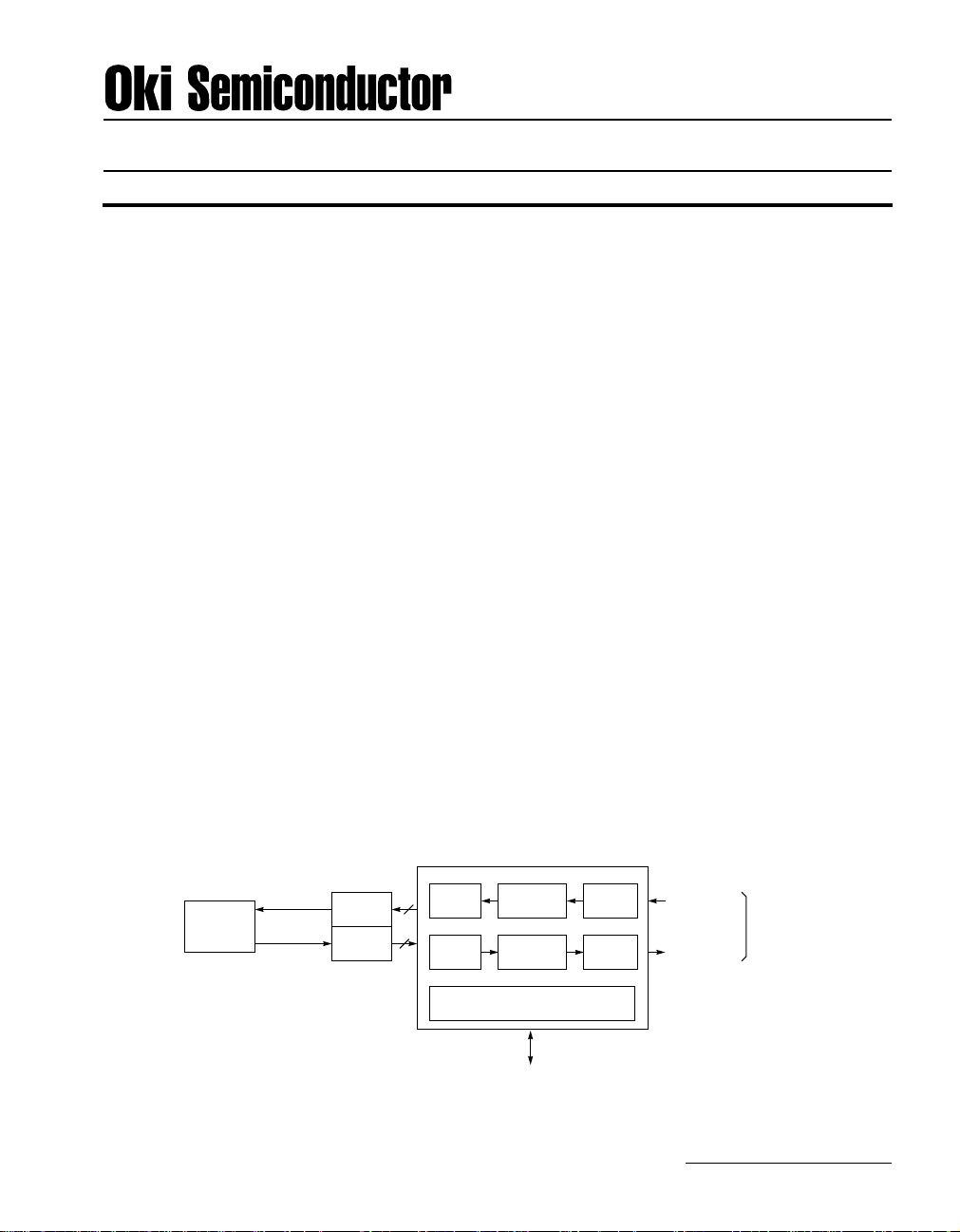
shows a typical STS-12/12c application using the TC-622Pro/Pro+.
• Separate performance monitors for individual cell
processors
• Line and Path alarm indication signal inserted into
the transmit signal
• Loss of signal (LOS), loss of frame synchronization
(LOF), loss of pointer (LOP), and loss of cell
delineation (LCD) conditions detected in the
incoming signal
• Transmit processor handles single or octet-wide cell
streams
• 176-pin LQPF package for both devices
Optical
Transceiver
TxD
RxD
Framer
Framer
Microprocessor Interface
PCI Bus (TC-622Pro)
MPI Bus (TC-622Pro+)
TC-622Pro/Pro+
Transmit Core
Logic
Receive Core
Logic
Transmit
UTOPIA
Receive
UTOPIA
External
Converter
Parallel
to Serial
Serial to
Parallel
Transmit
8
Receive
8
Figure 1. Typical STS12/12c Application
TxData [15:0]
ATM Layer Line Data
RxData [15:0]
1Oki Semiconductor
Page 8
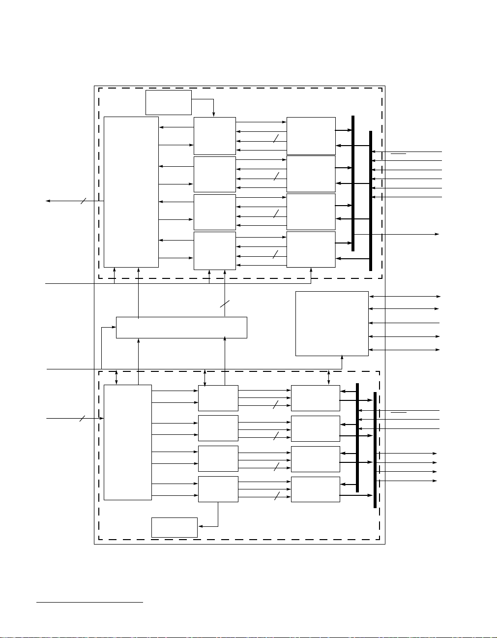
■
ML53301/ML53311 TC-622Pro/Pro+ ■ –––––––––––––––––––––––––––––––––––––––––––––––––––––––––––––
Test Cell
TxLINEDATA[7:0]
TxBYTECLK
Generators (4)
cell_data
enable
Transmit
Framer
and
Overhead
Processor
8
cell_data
enable
cell_data
enable
cell_data
enable
Rx Feedback to Tx
Synchronizer
Transmit
Cell
Processor
Transmit
Cell
Processor
Transmit
Cell
Processor
Transmit
Cell
Processor
Transmit Block
General Flow Control
4
Feedback
enable
SoC
data
cellpresent
enable
SoC
data
cellpresent
enable
SoC
data
cellpresent
enable
SoC
data
cellpresent
Transmit
8
UTOPIA
Transmit
8
UTOPIA
Transmit
8
UTOPIA
Transmit
UTOPIA
8
PCI Interface
(TC-622Pro)
or
MPI Interface
(TC-622Pro+)
TxCLK
TxENB
TxADDR[4:0]
TxDATA[15:0]
TxSOC
TxPRTY
TxCLAV
PCI_AD[31:0]
Control Bus
Clocks
MPI_ ADDR[6:0]
MPI_DATA[15:0]
RxBYTECLK
RxLINEDATA[7:0]
8
Rx Framer
and Overhead
Processor
2 Oki Semiconductor
cell_data
data valid
cell_data
data valid
cell_data
data valid
cell_data
data valid
Test Cell
Analyzers (4)
Rx Cell
Processor
Rx Cell
Processor
Rx Cell
Processor
Rx Cell
Processor
enable
SoC
data
enable
SoC
data
enable
SoC
data
enable
SoC
data
Receive Block
Rx UTOPIA
8
Rx UTOPIA
8
Rx UTOPIA
8
Rx UTOPIA
8
Figure 2. TC-622Pro/Pro+ Block Diagram
RxCLK
RxENB
RxADDR[4:0]
RxDATA[15:0]
RxSOC
RxPRTY
RxCLAV
Page 9

––––––––––––––––––––––––––––––––––––––––––––––––––––––––––––– ■ ML53301/ML53311 TC-622Pro/Pro+
3. KEY FEATURES
■
This section describes some of the features of the block shown in the block diagram in
Figure 2
3.1 T ransmit Test Cell Generator
• Four separate test cell generators, one for each of the four transmit cell processors
• Alternate source of idle cells for transmit cell processors
• Programmable cell header
• Random payload
• Counts number of test cells transmitted
3.2 Receive Test Cell Analyzer
• Four separate test cell analyzers
• Test cells filtered
• Programmable cell header
• Counts number of bit errors detected in payload
• Counts number of test cells received
3.3 Transmit Cell Processor
• Handles single or quad octet-wide cell streams
• Accepts both 52-byte cells, computes and inserts Header Error Check (HEC)
• Always adds coset polynomial (X
• Cell rate adaptation—inserts idle cells when no cell is available from the UTOPIA or FIFO
• Optionally inserts cells from an internal test cell generator in the place of idle cells
• Flow control—halts valid cell transmission when Generic Flow Control (GFC) is enabled
• Scrambles cell payload using the X
• Counts assigned and idle cells
6
+ X4 + X2 + 1)
43
+ 1 polynomial. Contains a self-synchronizing scrambler
.
3.4 Receive Cell Processor
• Handles single or quad octet-wide cell streams
• Cell delineation state machine
• Cell delineation using HEC
• Hunt, Pre-Sync, Sync, LCD defect, LCD Defect Pre-Sync, LCD Defect Verify, and LCD Failure
Verify states
• Correction and Detection states within Sync state
• Single- and multiple-bit error detection
• Single-bit error correction if correction is enabled
• Cell payload de-scrambling
• Idle cells discarded
• Performance Monitors
- Discarded cell (due to HEC violation, when in Sync state) counter
- Assigned and Idle cell counters
3Oki Semiconductor
Page 10

■
ML53301/ML53311 TC-622Pro/Pro+ ■ –––––––––––––––––––––––––––––––––––––––––––––––––––––––––––––
3.5 STS-12/12c Line Interface
• 8-bit parallel input and output
• 77.76 MHz clock
3.6 STS-12/12c Transmit Framer
• Timing control
- External timing reference—77.76 MHz clock
- A pulse given out for every frame transmitted
• STS-12/12c Pointer Insertion
- Normal mode
- No pointer increment
- No pointer decrement
- No NDF insertion
- Pointer value—620A
• Path Alarm Indication Signal (P-AIS) insertion on user command
• Path Remote Defect Indication (P-RDI) insertion on user command and on receiver alarm conditions
• Line AIS (L-AIS) insertion on user command
• Line RDI (L-RDI) insertion on user command and on receiver alarm conditions
• Path overhead insertion
• Section overhead insertion
• Line overhead insertion
• Fixed Stuff insertion in the case of STS-12c
- Fixed value inserted (00hh)
• Frame scrambling according to the ITU-T I.432 standard
3.7 STS-12/12c Receive Framer
• Framing
- Loss of signal state machine (LOS)
- Parallel Frame Search, Byte-alignment
- Out of frame state machine (OOF)
- Loss of frame state machine (LOF)
- A pulse for every received frame given out
• Automatic Protection Switching (APS) bytes (K1, K2) written into registers
• Section Overhead Processing
- B1 parity error counter
• Line Overhead Processing
- B2 parity error frames counter
- Line AIS state machine
- Line RDI state machine
- Line FEBE accumulator
• STS-12/12c Pointer Tracking
- H1, H2 state machines
4 Oki Semiconductor
Page 11

––––––––––––––––––––––––––––––––––––––––––––––––––––––––––––– ■ ML53301/ML53311 TC-622Pro/Pro+
- NDF detection
- New pointer when three consecutive valid pointers are identical
- Pointer increment
- Pointer decrement
- Detection of invalid pointer (value > 782)
- Loss of Pointer (LOP) state machine
- Path AIS state machine
- Handles SONET/SDH modes as set by a register bit
• Fixed Stuff extraction
• 4 POH Processors
• Path overhead processing
- C2 byte—number of mismatches counted
- Path FEBE accumulated
- Path RDI state machine
- B3 parity error counter
3.8 PCI Bus Interface (TC-622Pro)
• Supports industry-standard 32-bit PCI data path at 33 MHz
• Provides even parity for data and address
• Multiplexed address/data architecture reduces pin count
• Supports multiple families of microprocessors
■
3.9 MPI Bus Interface (TC-622Pro+)
• Supports 16-bit MPI data path at 33 MHz
• Geared toward low cost applications
• Supports multiple families of microprocessors
3.10 Transmit and Receive UTOPIA
• Complete compliance with UTOPIA Level 2 Version 1.0 specifications for Multi-PHY (MPHY)
• Four UTOPIA ports with separate 4-cell rate matching buffers
• 50-MHz operation
• 16-bit wide data path
• MPHY operation with single TxCLAV and RxCLAV status signals
• Support of 52-byte and 53-byte cells
• Discarding of runt cells
• Optional discarding of cells with parity errors on transmit side
• Parity computation on receive side
5Oki Semiconductor
Page 12

■
ML53301/ML53311 TC-622Pro/Pro+ ■ –––––––––––––––––––––––––––––––––––––––––––––––––––––––––––––
4. FUNCTIONAL DESCRIPTION
This section is divided into the following subsections:
• Section 4.1, "Architectural Overview": Defines each block in
• Section 4.2, "Transmit Architecture": Discusses the operation of the Transmit module
• Section 4.3, "Receive Architecture": Discusses the operation of the Receive module
• Section 4.4, "PCI Bus Architecture (TC-622Pro)": Provides a brief overview of the ML53301 TC622Pro PCI Bus Interface
• Section 4.5, "MPI Bus Architecture (TC-622Pro+)": Provides a brief overview of the ML53311 TC622Pro+ low-cost MPI Bus interface.
Throughout this data sheet there are references to SONET frames and ATM cells. For an overview on
SONET frames and ATM cell structures, refer to Section 10.
4.1 Architectural Overview
This section defines the logic blocks shown in the block diagram in
4.1.1 Transmit Framer and Overhead Processor
The transmit framer contains a frame generator, transportation overhead generator, path overhead generator, and a frame scrambler. The transmit framer generates the actual STS-12 or STS-12c frame from
ATM cells received from the transmit cell processors. In addition to the Synchronous Payload Envelope
(SPE) which contains the actual data, each 9720-byte SONET frame consists of a 324-byte
Overhead
The
byte
toring and voice communication. The
to the start of the synchronous payload envelope (SPE), SPE frequency adjustment, error monitoring and
automatic protection switching.
The
support path error monitoring, connection continuity verification, monitoring of the end-to-end path
performance, and STS-1 frame status.
The Frame Scrambler scrambles the SONET frame using a frame synchronous scrambler implementing a
specific polynomial. Frames are scrambled to minimize the possibility of payload data looking like a
header pattern and simplifies the frame recovery process at the destination.
For more information on these overheads, refer to Section 10, "SONET Frames and ATM Cell Structure".
and 9-byte or 36-byte
Transportation Overhead
Line overhead
Path overhead
. The
Section overhead
(POH) generator contains 9 bytes that form the first column of the SPE. These bytes
Path Overhead
.
(TOH) is 324 bytes in size and contains a 108 byte
generator includes bytes for frame synchronization, error moni-
Line overhead
generator consists of 216 bytes that include pointers
Figure 2
Figure 2
.
Section overhead
Transportation
and an 216
4.1.2 Transmit Cell Processors
The TC-622Pro/Pro+ consists of four transmit cell processors. All four processors are enabled in STS-12
mode. Only one processor is enabled in STS-12c mode. The two main functions of each transmit cell processor are cell rate adaptation and Header Error Check (HEC) byte insertion. If the UTOPIA FIFO does
not contain one or more complete cells, the cell processor inserts idle cells to achieve the correct cell adaptation. The HEC computation block computes the HEC byte from the first four bytes of any cell using a
special algorithm. The cell processor also counts the number of assigned cells transmitted as well as the
number of idle cells inserted. For more information on the transmit cell processor, refer to Section 4.1.2,
"Transmit Cell Processors".
6 Oki Semiconductor
Page 13

––––––––––––––––––––––––––––––––––––––––––––––––––––––––––––– ■ ML53301/ML53311 TC-622Pro/Pro+
4.1.3 Transmit UTOPIA
The Transmit UTOPIA consists of four identical ports, one for each transmit cell processor. Each UTOPIA
has a unique programmable port address. The function of each port is to facilitate the transfer of data
between the transmit cell processors and the ATM layer device.
4.1.4 Test Cell Generator
There are four test cell generators, one for each of the four transmit cell processors. The test cell generator
provides a source for idle cells as well as test cells. Whenever a cell processor does not have an assigned
cell to transmit, it reads an idle cell from the corresponding test cell generator. Test cells can also be
inserted into the data stream without interrupting the normal flow of data and are used for monitoring
purposes and to help maintain data integrity.
4.1.5 Receive Framer and Overhead Processor
The receive framer accepts non-aligned bytes from an external serial to parallel converter and extracts the
frame payload. The receive framer performs frame synchronization, synchronous payload envelope
extraction, overhead processing to detect alarm and error conditions, and performance monitoring.
4.1.6 Receive Cell Processors
The TC-622Pro/Pro+ contains four receive cell processors. All four processors are enabled in STS-12
mode. Only one processor is enabled in STS-12c mode. The processor delineates data received from the
receive framer to form cells. It computes the Header Error Check (HEC) over the first four bytes, compares it with the received HEC byte, and discards idle cells. The receive cell processor also counts the
number of assigned cells written to the UTOPIA FIFO and the number of idle cells dropped.
■
4.1.7 Test Cell Analyzer
There are four test cell analyzers, one for each of the four receive cell processors. Whenever a cell processor receives a cell with the header pattern matching one that is programmed for test cells, that cell is
passed to the corresponding Test Cell Analyzer instead of the UTOPIA FIFO.
4.1.8 Receive UTOPIA
The Receive UTOPIA consists of four identical ports, one for each Receive Cell processor. Each UTOPIA
has a unique port address. The function of each port is to facilitate the transfer of data between the
Receive Cell processors and the ATM layer device.
4.1.9 PCI Bus Interface (TC-622Pro)
The TC-622Pro contains an industry-standard PCI interface that allows the host to read and write the TC622Pro registers using a standard on-chip microprocessor. The PCI interface contains signal translation
logic that interfaces to the PCI bus signals and generates TC-622Pro register control signals. A parity calculator calculates even parity over the address, data, and command busses, and the byte enables. The
interrupt manager receives interrupts from the TC-622Pro and generates a corresponding interrupt on
the PCI bus. The byte swap block swaps the address bytes depending on the Little Endian/Big Endian
requirements of the host. Refer to Section 8 for more information on the PCI bus interface.
7Oki Semiconductor
Page 14
■
ML53301/ML53311 TC-622Pro/Pro+ ■ –––––––––––––––––––––––––––––––––––––––––––––––––––––––––––––
4.1.10 MPI Bus Interface (TC-622Pro+)
The TC-622Pro+ provides a generic microprocessor interface (MPI) intended for use in low-cost applications where a full PCI interface is not required. In the TC-622Pro+, registers are accessed directly by driving the required address onto the bus. No memory mapping of registers is required. In the TC-622Pro
(PCI) the registers are memory-mapped to a specific 8-kbyte space. In the TC-622Pro+ (MPI) the registers
are not memory mapped and are accessed directly using a separate 7-bit address bus.
Refer to Section 9 for more information on the MPI bus interface.
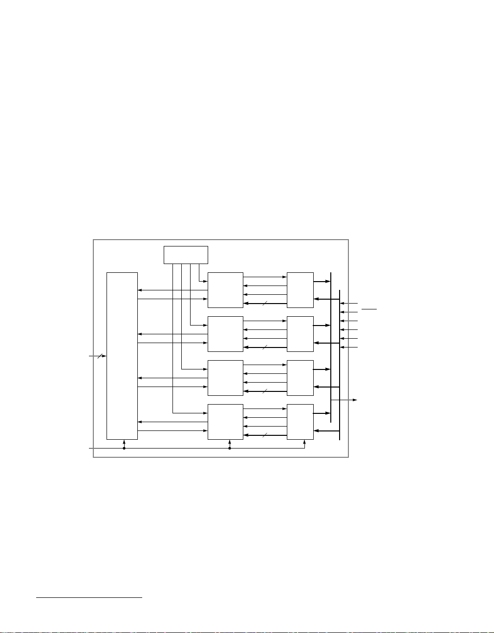
4.2 Transmit Architecture
The TC-622Pro/Pro+ block diagram in
receive interface, and PCI/MPI interface. This section discusses the transmit interface. Refer to Section
4.3 for more information on the receive interface. Refer to Section 4.4 for more information on the PCI Bus
interface. Refer to Section 4.5 for more information on the MPI Bus interface.
gram of the transmit interface.
cell_data
enable
cell_data
enable
Tx Framer
TxLINEDATA[7:0]
TxBYTECLK
8
and OH
Processor
cell_data
enable
cell_data
enable
Figure 2
Test Cell
Generators (4)
is broken into three major interfaces; transmit interface,
Tx Cell
Processor
Tx Cell
Processor
Tx Cell
Processor
Tx Cell
Processor
Tx_Enable
Tx_CellPresent
Tx SoC
Tx _Data
8
Tx_Enable
Tx_CellPresent
Tx SoC
Tx _Data
8
Tx_Enable
Tx_CellPresent
Tx SoC
Tx _Data
8
Tx_Enable
Tx_CellPresent
Tx SoC
Tx _Data
8
Tx
UTOPIA
Tx
UTOPIA
Tx
UTOPIA
Tx
UTOPIA
Figure 3
shows a block dia-
TxCLK
TxENB
TxADDR [4:0]
TxDATA[15:0]
TxSOC
TxPRTY
TxCLAV
Figure 3. TC-622Pro/Pro+ Transmit Architecture Block Diagram
The transmit architecture in the TC-622Pro/Pro+ contains the following four modules below which are
discussed, along with the transmit data flow, in the following sections:
• Four Transmit UTOPIA channels
• Four Transmit Cell Processors
• Four Transmit Test Cell Generators
• Transmit Framer
8 Oki Semiconductor
Page 15
––––––––––––––––––––––––––––––––––––––––––––––––––––––––––––– ■ ML53301/ML53311 TC-622Pro/Pro+
4.2.1 Transmit Data Flow
During a transmit operation, ATM cells are written into the transmit UTOPIA buffers by the ATM layer
device. The transmit UTOPIA provides an industry standard ATM PHY interface. Four transmit UTOPIA buffers are provided to serve four independent ATM sources.
Once the ATM cells have been written to the PHY and placed in the cell buffers, they are read out by the
transmit cell processors. There are four processors, one for each transmit UTOPIA PHY. The transmit cell
processor calculates the HEC byte and inserts this information into byte 5 of the ATM cell header. The
cell payload is then scrambled to minimize the potential for false headers in the payload, and to avoid
deliberate transmission of line alarm patterns.
Once the entire cell has been processed it is passed to the transmit framer where a SONET STS-12/12c
frame, complete with section, line, and path overheads, is constructed from the stream of ATM cells. The
cell processor then reads another ATM cell from the transmit UTOPIA. If the UTOPIA cell buffer is
empty, the corresponding test cell generator inserts an idle cell into the transmit stream.
Figure 4
shows a flow diagram of a transmit operation for one transmit path. The other three paths are
identical.
■
Transmit cell
processor passes
processed cell to the
transmit framer.
TxLINEDATA[7:0]
TxBYTECLK
Transmit framer constructs STS12/12c SONET frame from ATM
cells. Section, line and path
overheads are generated by the
overhead processors and are
attached to each SONET frame.
Tx Framer and
OH Processor
Test Cell
Generator
TcEnable TestCell
cell data
enable
Tx Cell
Processor
Transmit cell processor
computes HEC byte and
inserts it into the ATM cell,
then scrambles payload.
Direction of Data Flow
Idle cells inserted by the test cell
generator if the transmit cell
buffer is empty.
Tx_Enable
Tx_CellPresent
Tx_SoC
Tx_Data
8
Transmit data read b y Tx
cell processor.
Tx Cell
Buffer
TxCLAV
TxCLK
TxENB
Tx UTOPIA
TxADDR[4:0]
TxDATA[15:0]
TxSOC
TxPRTY
ATM cells written to Tx UTOPIA cell FIFO
buffers.
Incoming
ATM Cells
Figure 4. Data Flow During a Transmit Operation
Microprocessor Interface to Transmit Architecture
The TC-622Pro/Pro+ contains a number of registers that contain performance monitoring, status, and
alarm indication information. These registers are accessed by the host through the PCI (TC-622Pro) or
MPI (TC-622Pro+) bus interface. Refer to Section 4.4 for more information on the PCI interface. Refer to
Section 4.5 for more information on the MPI Interface. Refer to Section 6 for a listing and description of
TC-622Pro/Pro+ registers.
9Oki Semiconductor
Page 16

■
ML53301/ML53311 TC-622Pro/Pro+ ■ –––––––––––––––––––––––––––––––––––––––––––––––––––––––––––––
Performance Monitors
The TC-622Pro/Pro+ maintains running counters that monitor various error events as they occur. These
counters are maintained within the transmit block and are not reset when read. Rather, a sticky bit is
used to indicate count roll-over. Four roll-over registers, located at addresses 0x52 - 0x55, are used to
store these sticky bit values. The user can read the appropriate roll-over register and reset the bit manually if desired.
The TC-622Pro/Pro+ transmit counters perform the following functions:
• Counts the number of cells and frames transmitted
• Counts the number of cells discarded because of multiple-bit errors
• Counts the number of idle cells inserted into the data stream to achieve cell rate adaptation
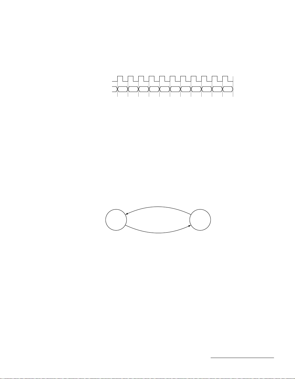
4.2.2 Transmit UTOPIA PHY
The TC-622Pro/Pro+ consists of four identical transmit UTOPIA PHY ports. Each port has a unique
address and supports a different ATM stream. The function of each port is to facilitate the transfer of data
between the transmit cell processors and the ATM physical layer. Each port conforms to the UTOPIA
Level 2 Version 1.0 specification and supports Multi-PHY (MPHY) operation using a 16-bit data path.
Operation with an 8-bit ATM cell path is not supported. In STS-12c mode only port 0 is active. The ATM
master device can transfer data by driving the address of that port on the
the
TxCLAV
ATM Layer Interface
output is driven permanently by that port only.
TxADDR[4:0]
lines such that
The transmit interface is controlled by the ATM layer. This layer provides an interface clock to the UTOPIA PHY for synchronizing all interface transfers. The transmit interface has data flowing in the same
direction as the ATM enable. The following UTOPIA interface signals;
DDR[4:0], TxSOC
, and
TxPRTY,
are all sampled on the rising edge of
TxENB
TxCLK.
, TxDATA[15:0], TxA-
The UTOPIA slave controls the flow of data through the TxCLAV signal. Once this signal is asserted, the
ATM layer responds by driving data onto TxDATA[15:0] and asserting TxENB
.
Figure 5, Figure 6, and Figure 7 show three different conditions under which data is transmitted.
1 2 3 4 5 6 7 8 9 10 11 12 13 14 15 16 17 18 19 20
TxCLK
TxADDR[4:0]
TxCLAV
TxENB
TxDATA[15:0]
TxSOC
Cell transmission
N +1 1F N 1F N +3 1F N +2 1F N-1 1F N 1F N +3 1F N +3 1F N -2 1F N -3
Hi-Z N+1 Hi-Z Hi-Z N+3Hi-Z Hi-Z Hi-Z Hi-Z Hi-Z Hi-Z Hi-Z N N+3 N+2 N-1 N N+3 N-2 N-3
P35 P36 P37 P38 P39 P40 P41 P42 P43 P44 P45 P46 P47 P48 H1 H2 H3 H4
to
Figure 5. Polling Phase and Selection Phase at Transmit Interface
10 Oki Semiconductor
PHY N PHY N +3
Page 17
––––––––––––––––––––––––––––––––––––––––––––––––––––––––––––– ■ ML53301/ML53311 TC-622Pro/Pro+ ■
1 2 3 4 5 6 7 8 9 10 11 12 13 14 15 16 17 18 19 20
TxCLK
TxADDR[4:0]
TxCLAV
TxENB
TxDATA[15:0]
TxSOC
Cell Transmission
TxCLK
TxADDR[4:0]
TxCLAV
TxENB
TxDATA[15:0]
TxSOC
Cell transmission
N +1 1F N 1F N +3 1F N +2 1F N-1 1F N 1F N +3 1F N +3 1F N -2 1F N -3
Hi-Z N+1 Hi-Z Hi-Z N+3Hi-Z Hi-Z Hi-Z Hi-Z Hi-Z Hi-Z Hi-Z N N+3 N+2 N-1 N N+3 N-2 N-3
P45 P46 P47 P48 H1 H2 H3 H4
Hi-Z
to
PHY N PHY N +3
Figure 6. End and Restart of Cell Transmission at Transmit Interface
1 2 3 4 5 6 7 8 9 10 11 12 13 14 15 16 17 18 19 20
N +1 1F N 1F N +3 1F N +2 1F N-1 1F N 1F N +3 1F M 1F N -2 1F N -3
Hi-Z N+1 Hi-Z Hi-Z N+3Hi-Z Hi-Z Hi-Z Hi-Z Hi-Z Hi-Z Hi-Z N N+3 N+2 N-1 N N+3 N-2 N-3
P45 P46 P47 P48 H1 H2 H3 H4
Hi-Z
to
PHY M PHY M
pause and transmission
Figure 7. Transmission to PHY Paused for 11 cycles
Transmit Cell Processor Interface
Each of the four transmit cell processors provides an interface clock to the UTOPIA slave block for synchronizing all interface transfers. The cell processor generates all signals on the rising edge of an internal
cell processor signal clock.
Once at least one or more ATM cells have been received from the ATM layer and stored to the UTOPIA
cell buffer, the UTOPIA indicates to the cell processor that cell data is ready for transfer. The cell processor uses internal handshake signals to control the flow of data between the UTOPIA and the cell processor.
4.2.3 Transmit Cell Processor
The TC-622Pro/Pro+ contains four transmit cell processors which operate independently of one another.
Each transmit cell processor performs two primary functions; Header Error Check (HEC) insertion and cell
rate adaptation.
The TC-622Pro/Pro+ supports two SONET frame modes which determine how many processors are
enabled. In STS-12 mode, all four cell processors are enabled and one at a time is selected. The four pro-
11Oki Semiconductor
Page 18

■ ML53301/ML53311 TC-622Pro/Pro+ ■ –––––––––––––––––––––––––––––––––––––––––––––––––––––––––––––
cessors are enabled in a fixed order. In STS-12c mode one processor is enabled and the other three are disabled. The UTOPIA PHY asserts the internal Tx_CellPresent signal to inform the cell processor that an
ATM cell is in the cell FIFO buffer and is ready for transmission. The cell processor asserts the internal
Tx_Enable signal and reads the 52-byte ATM cell from the FIFO. These signals are provided for clarity
and are not available externally.
Once the cell has been read, the HEC computation block computes the HEC based on the first four bytes
read from the FIFO using the CRC-8 polynomial (X
6
(X
+ X4 + X2 + 1). The coset is a derivative of the CRC-8 polynomial. In the TC-622Pro/Pro+ devices the
8
+ X2 + X + 1) and always adds the coset polynomial
coset polynomial is always enabled. The HEC computation is then inserted into the fifth byte position of
the cell, during which time the cell processor stops reading from the FIFO for one clock cycle. Except for
the first five header bytes, the 48-byte cell payload is scrambled using a self-synchronizing scrambler
employing the polynomial (X
43
+ 1). Cell payloads are scrambled to minimize the possibility of payload
data looking like a header pattern. Scrambling the data helps simplify the frame recovery process at the
destination by increasing the level of differentiation between the header and the cell payload.
If the UTOPIA FIFO does not contain a complete cell, the cell processor inserts idle cells from the test cell
generator to achieve the correct cell rate adaptation. The idle cells have a fixed header pattern of 0x(00,
00, 00, 01, 52), and a fixed payload of (0x6A).
The cell processor can also send test cells from the test cell generator instead of idle cells. The header for
these test cells is programmed in registers. The processor computes the HEC of these test cells. When test
cells are inserted, availability of a cell in the FIFO is checked at the end of every cell. Anytime a full cell is
available in the FIFO, it is read by the cell processor and inserted into the data stream.
In addition to HEC computation and cell rate adaptation, the cell processor also counts the number of
assigned cells transmitted and the number of idle cells inserted. These counters are free-running and
indicate roll-over using a sticky-bit. Each counter register is 16-bits in size and uses a 17th bit to indicate
the roll-over status for that register. The sticky bits from each counter register are concatenated into a
series of 16-bit registers called ‘roll-over’ registers. These registers are located at addresses 0x52 - 0x55 in
TC-622Pro/Pro+ register address space.
The transmit cell processor receives general flow control (GFC) feedback from the receive cell processor.
When a GFC Halt is enabled by the user and the GFC feedback is received, the ATM cells are not
accepted and transmitted from the FIFO, even if cells in the FIFO are available for transmission.
4.2.4 Test Cell Generator
The TC-622Pro/Pro+ contains four transmit test cell generators, one for each transmit cell processor. The
test cell generators provide a source of idle cells for the corresponding cell processor. Whenever the cell
processor does not have assigned cells to read from the UTOPIA buffer, it reads idle cells from the test
cell generator in order to meet the correct cell rate adaptation.
When the internal TcEnable signal is asserted by the cell processor, the test cell generator places a test cell
on cell data bus in the following clock. The cell data is generated by a Pseudo Random Sequence Generator (PRBS). The PRBS is a shift register that generates a random number and then repeats the sequence
after some period of time. There are four different maximum-length polynomials used to ensure random
data for all of the four cell streams independent of one another.
• Polynomial 1 - (x
• Polynomial 2 - (x
• Polynomial 3 - (x
• Polynomial 4 - (x
12 Oki Semiconductor
22
+ X17 + 1)
22
+ X11 + 1)
22
+ X19 + 1)
22
+ X14 + 1)
Page 19

––––––––––––––––––––––––––––––––––––––––––––––––––––––––––––– ■ ML53301/ML53311 TC-622Pro/Pro+ ■
4.2.5 Transmit Framer And Overhead Processor
The transmit framer receives processed ATM cells from the cell processors and constructs an STS-12/12c
frame depending on the mode. Each STS frame contains a 108-byte section overhead, an 216-byte line
overhead, and a 9- or 36-byte path overhead, all of which contain information about the frame. This
information is calculated by the overhead processor within the transmit framer. Table 1 shows the values
generated for each overhead field by the overhead processors. All fields in Table 1 are 8-bits wide. Once
the entire frame is assembled, all bytes of the frame except the framing bytes (A1, A2, C1) are scrambled
using a frame synchronous scrambler that implements the polynomial (X
7
+ X6 + 1).
Refer to Section 10 for the definition and physical location of each field within the corresponding overhead.
Table 1. Transmit Overhead Values
Field Byte Type Value
Section Overhead Processor (9 bytes)
A1 Framing 0xF6
A2 Framing 0x28
C1 Identity SONET mode: 0x01, 0x02, ... 0x0C
B1 BIP-8 8-bit parity field. Value depends on data.
All others ---- Fixed at 0x00
Line Overhead Processor (18 bytes)
H1 Pointer STS-12 mode: First four bytes are 0x62.
H2 Pointer STS-12 mode: First four bytes are 0x0A.
H3 Pointer Action 0x00
B2 Parity Calculates 96-bit BIP parity over the line overhead and entire SPE before scrambling, then inserts the value into the
K1 APS AIS insertion: User command AIS code 0x07is inserted into the K1 byte.
K2 APS RDI insertion: User command RDI code 0x06is inserted into the K2 byte if one or more error conditions (LOS, LOF, LOC)
D4 - D12 Datacomm Fixed at 0x00
Z1 - Z2 Growth Fixed at 0x00
Path Overhead Processor (9 bytes)
J1 Trace Fixed at 0x00
B3 BIP - 8 8-bit parity value depends on data
C2 Signal label Fixed at 0x13
G1 Path status Path FEBE value is inserted in this byte
SDH mode: 0x01, 0x02, ... 0x04. Remaining 8 bytes = 0xCC
Remaining 8 bytes = 0x93.
STS-12c mode: First byte is 0x62.
Remaining 11 bytes are 0x93.
Remaining 8 bytes = H2*
STS-12c mode: First byte is 0x0A.
Remaining 11 bytes are H2*
*(H2 = 0xFF)
current frame. The actual value is data-dependent
are detected in the receiver.
13Oki Semiconductor
Page 20
■ ML53301/ML53311 TC-622Pro/Pro+ ■ –––––––––––––––––––––––––––––––––––––––––––––––––––––––––––––
Table 1. Transmit Overhead Values
Field Byte Type Value
F2 User channel Fixed at 0x00
H4 Multi-frame Fixed at 0x00
Z3 - Z5 Growth Fixed at 0x00
The transmit framer uses the TxBYTECLK Clock to transfer information to the external parallel-to-serial
converter. Transmit line data is transferred in 8-bit quantities at the rising edge of each TxBYTECLK.
Figure 8 shows a timing diagram of a typical line data transfer. Note that the acronym P2S in the diagram
below is for the ‘Parallel-to-Serial’ converter.
TxBYTECLK
TxLINEDATA[7:0]
(from framer to
P2S converter)
D1 D2 D3 D4 D5 D6 D7 D8 D9 D10 D11
Figure 8. Transmit Line Interface Timings
4.3 Receive Architecture
The receive architecture in the TC-622Pro/Pro+ contains the following four modules below which are
discussed, along with the receive data flow, in the following sections:
• Receive Framer and Overhead Processor
• Four Receive Test Cell Analyzers
• Four Receive Cell Processors
• Four Receive UTOPIA’s
The TC-622Pro/Pro+ block diagram in Figure 2 is broken into three major interfaces; transmit interface,
receive interface, and PCI/MPI interface. This section discusses the architecture of the receive interface.
Refer to Section 4.2 and Section 4.4 for more information on the transmit and PCI (TC-622Pro) interfaces.
Refer to Section 4.5 for more information on the TC-622Pro+ MPI interface. Figure 9 shows a block diagram of the receive architecture.
14 Oki Semiconductor
Page 21
––––––––––––––––––––––––––––––––––––––––––––––––––––––––––––– ■ ML53301/ML53311 TC-622Pro/Pro+ ■
Test Cell
Analyzers (4)
Rx_Enable
Rx_SoC
Rx _Data
8
Rx_Enable
Rx_SoC
Rx _Data
8
Rx_Enable
Rx_SoC
Rx _Data
8
Rx_Enable
Rx_SoC
Rx _Data
8
Rx
UTOPIA
Rx
UTOPIA
Rx
UTOPIA
Rx
UTOPIA
RxCLK
RxENB
RxADDR[4:0]
RxDATA[15:0]
RxSOC
RxPRTY
RxCLAV
RxLINEDATA[7:0]
RxBYTECLK
8
Rx Framer
and OH
Processor
spe_data
data_valid
spe_data
data_valid
spe_data
data_valid
spe_data
data_valid
Rx Cell
Processor
Rx Cell
Processor
Rx Cell
Processor
Rx Cell
Processor
Figure 9. Receive Architecture Block Diagram
4.3.1 Receive Data Flow
During a receive operation, the incoming serial bit stream is converted into bytes by an external serial-toparallel converter and driven to the receive framer on RxLINEDATA[7:0]. This 8-bit value is not bytealigned when it enters the framer and the framer must search the byte stream for the framing pattern.
Once the framing pattern is located, frame synchronization is declared and the byte boundaries of the
received data are determined.
Each of the three overhead processors (section, line, and path) contained in the receive framer processes
the corresponding overhead bytes. The Synchronous Payload Envelope (SPE) contained in the frame is
extracted and passed to the receive cell processor. The receive framer detects various error conditions
and alarm indications in the incoming signal.
The cell processor performs cell delineation using the Header Error Control (HEC) bytes and extracts the
appropriate cells. All cells with multiple-bit errors are discarded along with all idle cells. The cell processor descrambles the cell payload and writes the cell into the receive UTOPIA cell buffer.
Once the cells have entered the buffer, the receive UTOPIA indicates the availability of these cells to the
ATM layer, where they are subsequently read out by the ATM layer device.
Figure 10 shows a flow diagram of a receive operation.
15Oki Semiconductor
Page 22
■ ML53301/ML53311 TC-622Pro/Pro+ ■ –––––––––––––––––––––––––––––––––––––––––––––––––––––––––––––
Receive framer passes
processed SPE data to
the Rx cell processor.
RxLINEDATA[7:0]
RxBYTECLK
Receive framer receives STS12/12c SONET frame and
processes the section, line, and
path overheads. The framer
searches for the framing pattern,
then byte-aligns and synchronizes
the frame.
Test Cell
Analyzer
Tc Enable Test Cell
Rx Framer
8
and OH
Processor
SPE Data
Enable
Rx Cell
Processor
Receive cell processor
performs cell delineation
using the HEC bytes,
descrambles the payload,
and extracts the ATM cells.
Direction of Data Flow
Test cells are e xtracted from the
byte stream and passed to the
test cell analyzer.
Rx_Enable
Rx_SoC
Rx_Data
Rx Cell
Buffer
8
Processed data are
passed to the Rx
UTOPIA cell FIFO buffer.
RxCLAV
RxCLK
RxENB
Rx UTOPIA
RxADDR[4:0]
RxDATA[15:0]
RxSOC
RxPRTY
ATM cells are written to the cell buff er by
the cell processor. The Rx UTOPIA then
indicates to the ATM layer device that
cells are available. The ATM layer device
controls when the data is transferred.
Outgoing
ATM Cells
Figure 10. Data Flow During a Receive Operation
Microprocessor Interface to Receive Architecture
The TC-622Pro/Pro+ contains a number of registers containing performance monitoring, status, and
alarm indication information. In the ML53301 TC-622-Pro device, these registers are accessed by the host
through the PCI bus. In the ML53311 TC-622Pro+ device, these registers are accessed directly through
the MPI Bus Interface. Refer to Section 4.4 for more information on the PCI interface. Refer to Section 4.5
for more information on the MPI Interface. Refer to Section 6 for a listing and description of TC-622Pro
registers.
Performance Monitors
The TC-622Pro/Pro+ maintains running counters that monitor various error events as they occur during
a receive operation. These counters are maintained within the receive block and are not reset when read.
Rather, a sticky bit is used to indicate count roll-over. The sticky bits for all counter registers are concatenated together into four 16-bit registers that are located at addresses 0x52 - 0x55. The user can read the
appropriate roll-over register and reset the bit manually if desired.
The TC-622Pro/Pro+ counters perform the following functions:
• Counts the number of cells and frames received
• Counts the number of cells discarded because of multiple-bit errors
• Counts the number of B1, B2, and B3 parity errors detected in the incoming signal. B1 corresponds
to errors detected in the section overhead, B2 corresponds to errors detected in the line overhead,
and B3 corresponds to errors detected in the path overhead.
• Counts the number of line and path Far End Block Error (FEBE) values received.
16 Oki Semiconductor
Page 23

––––––––––––––––––––––––––––––––––––––––––––––––––––––––––––– ■ ML53301/ML53311 TC-622Pro/Pro+ ■
4.3.2 Receive Framer And Overhead Processor
The receive framer receives byte line data after the bit stream has been converted using an external serialto-parallel converter. The receive framer takes in non-aligned bytes and extracts the frame payload. In
STS-12c mode only one of the four processor modules is active, hence there is only one payload (SPE) to
extract. In STS-12 mode the framer extracts four independent payloads. The receive framer performs the
following functions:
• STS-12/12c frame recovery and synchronization
• Pointer processing to extract the Synchronous Payload Envelope (SPE)
• Overhead processing to detect alarm conditions in the incoming signal
• Performance monitoring
Each of these functions is explained in the following sections.
Frame Recovery and Synchronization
Data entering the receive framer is stored in a 31-bit buffer where the framer searches for the framing
patterns. During normal frame transmission the framer is in the ‘sync’ state and expects twelve 0xF6 values followed immediately by twelve 0x28 values at a fixed location within the buffer. Each of these values must be received exactly 125 µs apart, the duration of a typical SONET frame. Once these patterns are
found, that portion of the buffer is used to give out the byte-aligned data. When the framer detects an
out-of-frame condition, it searches for a pattern equivalent to 0x6F6282. A change of byte alignment
occurs only when the receive framer makes a transition from the Out-Of-Frame (OOF) state to the Sync
state.
Out-Of-Frame State Machine
The OOF state machine is used to monitor the out-of-frame condition and is set whenever there are four
consecutive incorrect framing patterns. The machine is reset once two consecutive correct patterns are
observed. Figure 11 shows a diagram of the OOF state machine.
Two consecutive correct
framing patterns (Sync)
Sync (correct)
framing patterns
Reset Set
Four consecutive incorrect
framing patterns
Figure 11. Out-Of-Frame State Machine
Loss-Of-Frame State Machine
The OOF condition above is generated at 125 µS intervals. This is the rate at which the framing patterns
are extracted by the receive framer. If 24 consecutive frames (3 mS) generate an OOF condition, the LOF
state machine is set. The LOF state machine is reset after 8 frames (1 mS) of continuous Sync condition
(no OOF condition). Figure 12 shows a diagram of the LOF state machine.
17Oki Semiconductor
Page 24

■ ML53301/ML53311 TC-622Pro/Pro+ ■ –––––––––––––––––––––––––––––––––––––––––––––––––––––––––––––
Eight consecutive
Sync frames (1mS)
Reset Set
24 consecutive OOF
frames (3 mS)
Figure 12. Loss-Of-Frame State Machine
Loss-of-Signal State Machine
The TC-622Pro/Pro+ implements a frame synchronous descrambler that implements the polynomial (X
7
+ X6 + 1) which is used to descramble the overheads and the cell payload. Note that framing bytes A1,
A2, and A3 of the section overhead are not descrambled. The descrambler is initialized at the start of each
frame.
The LOS state machine is set when the receive framer gets an external LOS indication. This external LOS
indication is logically OR’ed with an internally detected LOS and then used throughout the device. The
LOS state machine is set when at least 20 µS of continuous all zero non-descrambled inputs are detected.
The machine is reset when two correct framing patters are detected exactly 125 µS apart with no LOS set
condition in between. Figure 13 shows a diagram of the LOS state machine.
Two consecutiv e correct framing patterns with
no LOS set condition in between
Reset Set
20 µS of consecutive all-zero
non-descrambled input
Figure 13. Loss-Of-Signal State Machine
Loss-Of-Pointer State Machine
The LOP state machine is set when under any one of the following conditions:
• Three consecutive valid identical pointers are received in eight frames
• Eight consecutive NDF pointers are received
• Eight consecutive invalid pointers are received
The machine is reset when three consecutive identical valid pointers are received. Figure 14 shows a diagram of the LOP state machine.
18 Oki Semiconductor
Page 25

––––––––––––––––––––––––––––––––––––––––––––––––––––––––––––– ■ ML53301/ML53311 TC-622Pro/Pro+ ■
3 consecutive identical valid pointers
Reset Set
3 consecutive identical valid pointers received in 8 frames
+ 8 consecutive NDF pointers received
+ 8 consecutive invalid pointers received
Figure 14. Loss-Of-Pointer State Machine
Path AIS State Machine
The P-AIS state machine is set when three consecutive H1 and H2 bytes are all ones (invalid pointers).
The machine is reset when three consecutive identical valid pointers are received. Figure 15 shows a diagram of the Path-AIS state machine.
3 consecutive identical valid pointers
Reset Set
3 consecutive all ones on H1 and H2 bytes
Figure 15. Path-AIS State Machine
Synchronous Payload Envelope (SPE) Extraction
The line overhead processor examines the H1 and H2 bytes of the line overhead to locate the start of the
SPE. In STS-12 mode four pointers are processed and maintained. In STS-12c mode only one pointer is
processed. The following functions are performed to extract the SPE.
• Invalid Pointer Detection: An invalid pointer is declared when the received H1H2[9:0] decimal
value is either greater than 782, not persistent for three frames, or the NDF flag is set. This value is
comprised of all 8 bits of the H2 byte and the lower 2 bits of the H1 byte.
• NDF Detection: A New Data Flag (NDF) condition is declared when bits [7:4] of the H1 byte match
one of the following patterns; 0001, 1000, 1001, 1011, or 1101. If an NDF condition is detected with a
valid pointer, the current pointer is changed to the received pointer which has the highest priority.
The NDF is a mechanism that provides for the sudden change in data alignment in a SONET frame.
• Three Consecutive Identical Pointers Detection: The occurrence of three consecutive identical
valid pointers is used to change the current pointer. This has the second highest priority after NDF.
• Justification Detection: The TC-622Pro/Pro+ supports both positive and negative justification.
Positive justification is declared if the received H1H2[9:0] value, after the inversion of all evennumbered bits, matches with the inverted current pointer in at least 8 or more bits. Negative
justification is declared if the received H1H2[9:0] value, after inversion of all odd-numbered bits,
matches with the inverted current pointer in at least 8 or more bits.
19Oki Semiconductor
Page 26

■ ML53301/ML53311 TC-622Pro/Pro+ ■ –––––––––––––––––––––––––––––––––––––––––––––––––––––––––––––
Overhead Processing
The TC-622Pro/Pro+ devices contain section, line, and path overhead processors for extraction and processing of the section and line overheads of the SONET frame, and the path overheads of each SPE.
Table 2 lists the various bytes of each overhead and how they are handled in the TC-622Pro and TC622Pro+ devices.
Table 2. Receive Overhead Values
Field Byte Type Value
Section Overhead Processor (9 bytes)
A1 Framing Contains frame synchronization information.
A2 Framing Contains frame synchronization information.
C1 Identity Identifies each STS-1 within a SONET frame.
B1 BIP-8 8-bit parity field. Value depends on data. This 8-bit interleaved field is calculated over the com-
E1, F1, D1-D3 ---- Ignored.
Line Overhead Processor (18 bytes)
H1, H2 Pointers The processing of these bytes is discussed in the above section on “SPE Extraction”.
H3 Pointer Action If negative justification is declared then the H3 byte contains valid SPE data. Otherwise it is
B2 BIP-8 The 96-bit line bit-interleaved parity is calculated over the SPE and the line overhead bits. The
K1, K2 Pointer Action These bytes are written to a register for user purposes. Automatic Protection Switching (APS)
Z2 Growth If the value contained in the third received Z2 byte is less than 97 decimal it is accumulated in
Z1, E3, D4-D12 ---- Ignored.
Path Overhead Processor (9 bytes)
J1 Trace Ignored.
B3 BIP - 8 Used to calculate the 8-bit interleaved parity over the entire SPE. The result is compared with
C2 Signal label The received C2 byte is compared with a fixed value of 0x13. The number of mismatches is
G1 Path status If the received value of path FEBE contained in the G1 byte is less than 9, then it is accumu-
F2, H4, Z3-Z5 ---- Ignored.
plete frame before descrambling. The result is compared with the received B1 byte in the next
frame. The number of bit errors are accumulated. The accumulation of B1 errors is stopped
under OOF, LOF, LOS, and LOC conditions.
ignored. Justification is discussed in the above section on “SPE Extraction”.
result is compared with the received B2 byte in the next frame. The number of mismatches are
accumulated. The accumulation of B2 errors and FEBE feedback are stopped under OOF,
LOF, LOS, and LOC conditions.
is not supported in the TC-622Pro/Pro+.
a counter. Overflow of the counter is indicated by a sticky bit. Accumulation of the received line
FEBE is stopped under OOF, LOF, LOS, and LOC conditions.
the B3 byte of the next SPE. The number of bit errors are accumulated using a counter.
Counter overflow is indicated by a sticky bit. The accumulation of B3 errors and the FEBE feedback are stopped under OOF, LOF, LOS, LOC, LOP, and Path AIS conditions.
maintained in a 3-bit counter. Counter overflow is indicated by a sticky bit. The counting of C2
byte mismatches is stopped under OOF, LOF, LOS, LOC, LOP, and Path AIS conditions.
lated using a counter. Counter overflow is indicated by a sticky bit. The counting of path FEBE
is stopped under OOF, LOF, LOS, LOC, LOP, and Path AIS conditions.
20 Oki Semiconductor
Page 27
––––––––––––––––––––––––––––––––––––––––––––––––––––––––––––– ■ ML53301/ML53311 TC-622Pro/Pro+ ■
The receive framer uses the RxBYTECLK signal to transfer information between the receive framer and
the external converter. Receive line data is transferred in 8-bit quantities at the rising edge of each
RxBYTECLK. Figure 16 shows a timing diagram of a typical receive line data transfer. Note that the acronym S2P stands for ‘Serial-to-Parallel’.
RxBYTECLK
RxLINEDATA[7:0]
(from S2P to framer)
D1 D2 D3 D4 D5 D6 D7 D8 D9 D10 D11
Figure 16. Receive Line Interface Timing Example
Receive Overhead State Machines
There are three state machine associated with receive overhead processing. Two machines pertain to the
K2 byte in the line overhead, and one machine pertains to the G1 byte in the path overhead. Each of these
machines is explained below.
The Line-AIS state machine is used for detecting an alarm indication on the line side (remote end). The
machine is set (Line-AIS condition declared) when a Line-AIS code (111 in the lower 3-bits of the K2 byte
of the section overhead) is received for five consecutive frames. The machine is reset when a Line-AIS
code other than ‘111’ in the K2 byte is received for five consecutive frames. Figure 17 shows a diagram of
the Line-AIS state machine.
K2 ≠ 111 for five
consecutive frames
Reset Set
K2 = 111 for five
consecutive frames
Figure 17. Line-AIS State Machine
The Line-RDI state machine is used to detect a remote defect indication on the line side. The machine is
set (Line-RDI condition declared) when a Line-RDI code (110 in the lower 3-bits of the K2 byte in the section overhead) is received for five consecutive frames. The machine is reset when a Line-RDI code other
than ‘110’ in the K2 byte is received for five consecutive frames. Figure 18 shows a diagram of the LineRDI state machine.
21Oki Semiconductor
Page 28

■ ML53301/ML53311 TC-622Pro/Pro+ ■ –––––––––––––––––––––––––––––––––––––––––––––––––––––––––––––
K2 ≠ 110 for five
consecutive frames
Reset Set
K2 = 110 for five
consecutive frames
Figure 18. Line-RDI State Machine
The Path-RDI state machine is used for remote defect indication in the path overhead. The machine is set
(Path-RDI condition declared) when a path RDI indication in the G1 byte (bit 5) of the path overhead is
received for ten consecutive frames. The machine is reset when no path RDI indication in the G1 byte is
received for ten consecutive frames. Figure 19 shows a diagram of the Path-RDI state machine.
G1 ≠ Path-RDI for ten
consecutive frames
Reset Set
G1 = Path-RDI for ten
consecutive frames
Figure 19. Path-RDI State Machine
4.3.3 Receive Cell Processor
The TC-622Pro/Pro+ contains four receive cell processors which operate independently of one another.
In STS-12 mode all four processors are enabled. In STS-12c mode only one processor is enabled and it
writes to only one UTOPIA channel. All receive cell processors operate in an identical manner.
The receive cell processor receives data from the receive framer and delineates the data to form ATM
cells. The processor descrambles delineated cells using a self-synchronizing descrambler that uses the
polynomial (X
43
+ 1). The cell delineation state machine computes the Header Error Control (HEC) over
the first four bytes of each ATM cell and compares it with the received HEC byte. The processor is capable of correcting single-bit errors in a cell header and detecting multi-bit errors. Idle cells are discarded.
The first four bits of each ATM cell header (in UNI mode) are the Generic Flow Control (GFC) bits.
Each cell processor counts the number of assigned cells written to the UTOPIA FIFO and the number of
idle cells dropped. It also counts the number of cells with multiple-bit HEC errors and the number of
transitions from the Sync state to the Out-of-Cell-Delineation state. The Sync state is declared when more
than seven ATM cells have been transmitted successfully. In this state the received ATM cells are
extracted and written to the FIFO. In the Out-of-Cell-Delineation state cells cannot be extracted. The state
machine transitions from the Sync state to the Out-of-Cell-Delineation state when more than 8 consecutive
ATM cells have an incorrect HEC value.
22 Oki Semiconductor
Page 29

––––––––––––––––––––––––––––––––––––––––––––––––––––––––––––– ■ ML53301/ML53311 TC-622Pro/Pro+ ■
4.3.4 Test Cell Analyzer
The TC-622Pro/Pro+ contains four test cell analyzers, one for each receive cell processor. Whenever a
cell processor receives a cell with a header pattern matching one that is programmed for test cells, that
cell is passed to the corresponding test cell analyzer and is not written to the UTOPIA FIFO. The test cell
analyzer uses the test cell to check the integrity of the payload and detect the number of bit errors
present. It also counts the number of test cells received. The test cell analyzer uses a pseudo-random generator that has two phases of operation.
• Phase 1: The test cell analyzer is synchronized to the incoming data.
• Phase 2: Once synchronization is achieved, the test cell analyzer detects all bit errors present in the
payload.
The PRBS polynomials used in the test cell analyzer give a maximum length random sequence. Four different polynomials are used to check data integrity for all four data streams from the four test cell analyzers.
• Polynomial 1 - (X
• Polynomial 2 - (X
• Polynomial 3 - (X
• Polynomial 4 - (X
22
+ X17 + 1)
22
+ X11 + 1)
22
+ X19 + 1)
22
+ X14 + 1)
The internal TcEnable signal from the cell processor qualifies the cell payload. Whenever TcEnable is
asserted the PBRS starts functioning. Note that this signal is not available external to the device.
4.3.5 Receive UTOPIA Phy
The TC-622Pro/Pro+ consists of four identical receive UTOPIA PHY ports. Each port has a unique
address and supports a different ATM stream. The function of each port is to facilitate the transfer of data
between the TC-622Pro/Pro+ receive cell processors and the ATM physical layer. Each port conforms to
the UTOPIA Level 2 Version 1.0 specification and supports Multi-PHY (MPHY) operation using a 16-bit
data path. MPHY mode indicates that all four UTOPIA ports on the TC-622Pro/Pro+ are active.
Operation with an 8-bit ATM cell path is not supported. If the ATM master intends to transfer data in
STS-12c mode where only port 0 is active, it can do so by driving the address of that port on the TxA-
DDR[4:0] lines such that the TxCLAV output is driven permanently by that port only.
ATM Layer Receive Interface
The receive interface is controlled by the ATM layer. This layer provides an interface clock to the UTOPIA PHY for synchronizing all interface transfers. The receive interface has data flowing in the opposite
direction as the ATM enable. The receive UTOPIA interface signals; RxENB
, RxDATA[15:0], RxA-
DDR[4:0], RxSOC, and RxPRTY, are all sampled or driven on the rising edge of RxCLK. The UTOPIA
slave controls the flow of data through the RxCLAV signal.
Figures 20 through 23 show three different conditions under which data is read from the receive UTOPIA
by the ATM layer device.
23Oki Semiconductor
Page 30
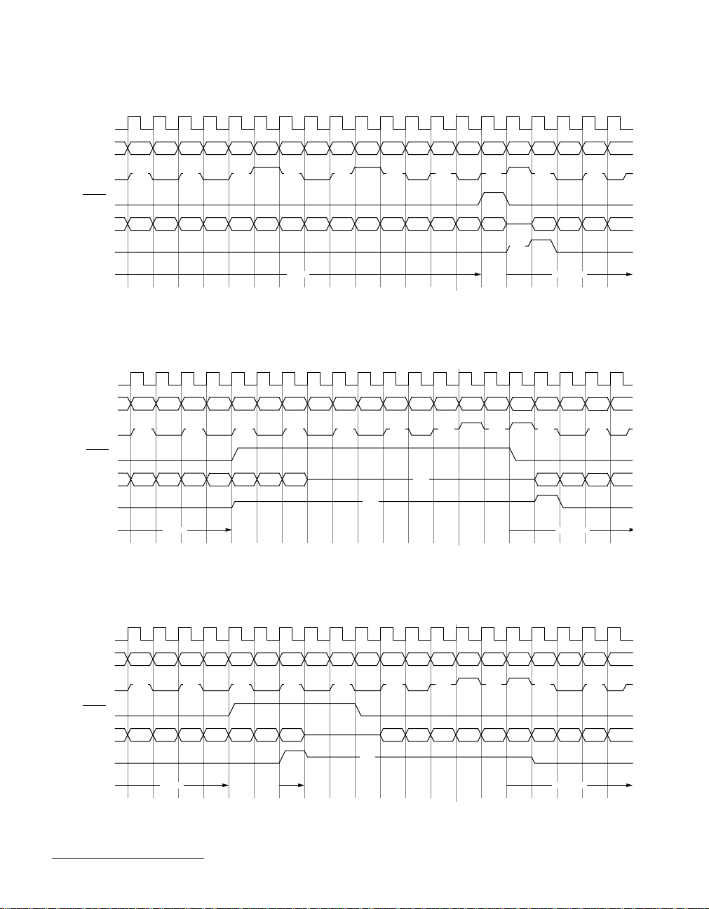
■ ML53301/ML53311 TC-622Pro/Pro+ ■ –––––––––––––––––––––––––––––––––––––––––––––––––––––––––––––
RxCLK
RxADDR[4:0]
RxCLAV
RxENB
RxDATA[15:0]
RxSOC
Cell transmission
RxCLK
RxADDR[4:0]
RxCLAV
RxENB
RxDATA[15:0]
RxSOC
Cell transmission
1 2 3 4 5 6 7 8 9 10 11 12 13 14 15 16 17 18 19 20
N +1 1F N 1F N +3 1F N +2 1F N-3 1F N 1F N +4 1F N +3 1F N -2 1F N -3
Hi-Z N+1 Hi-Z Hi-Z N+4Hi-Z Hi-Z Hi-Z Hi-Z Hi-Z Hi-Z Hi-Z N N+3 N+2 N-3 N N+3 N-2 N-3
P34 P35 P36 P37 P38 P39 P40 P41 P42 P43 P44 P45 P46 P47 H1 H2 H3
to
PHY N PHY N +3
P48
Hi-Z
Figure 20. Polling Phase and Selection Phase at Receive Interface
1 2 3 4 5 6 7 8 9 10 11 12 13 14 15 16 17 18 19 20
N +1 1F N +3 1F N 1F N +2 1F N-1 1F N 1F N +3 1F N +3 1F N -2 1F N -3
Hi-Z N+1 Hi-Z Hi-Z N+3Hi-Z Hi-Z Hi-Z Hi-Z Hi-Z Hi-Z Hi-Z N +3 N N+2 N-1 N N+3 N-2 N-3
P44 P45 P46 P47 H1 H2 H3
to
PHY N PHY N +3
P48 X X H4Hi-Z
Hi-Z
Figure 21. End and Restart of Cell Transmission at Receive Interface
RxCLK
RxADDR[4:0]
RxCLAV
RxENB
RxDATA[15:0]
RxSOC
Cell transmission
1 2 3 4 5 6 7 8 9 10 11 12 13 14 15 16 17 18 19 20
N+1 1F N 1F N 1F N+2 1F N 1F N -1 1F N+3 1F N+3 1F N-2 1F N-3
Hi-Z N+1 Hi-Z Hi-Z N+3Hi-Z Hi-Z Hi-Z Hi-Z Hi-Z Hi-Z Hi-Z N N+3 N+2 N N-1 N+3 N-2 N-3
P44 P45 P46 P47 H2 H3 H4
to
PHY N PHY N+3
Figure 22. Two Unexpected Back-to-Back Cells From the Same PHY Port
24 Oki Semiconductor
P48 X H1 H5 P1 P2 P3 P4 P5
Hi-Z
PHY N
Page 31
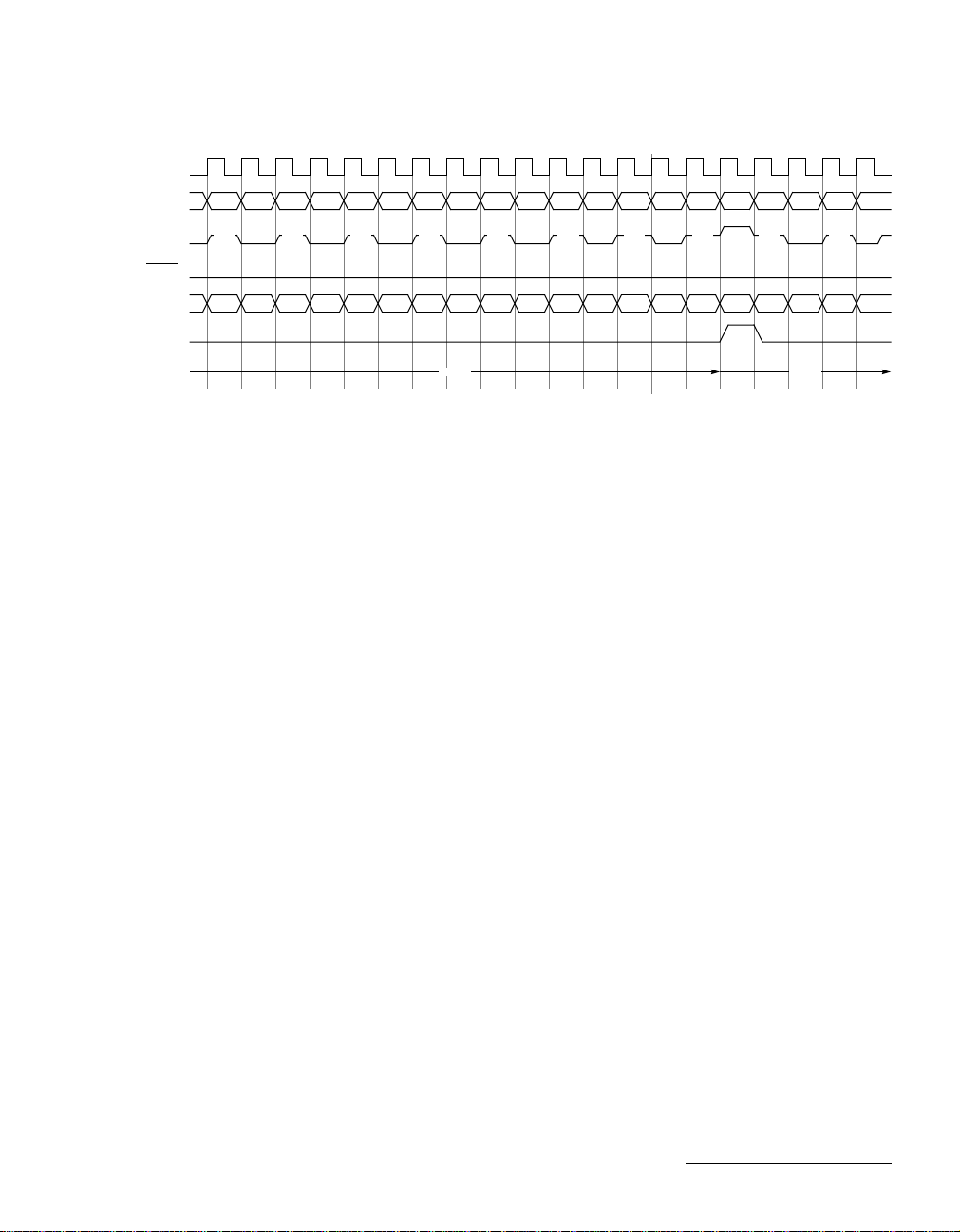
––––––––––––––––––––––––––––––––––––––––––––––––––––––––––––– ■ ML53301/ML53311 TC-622Pro/Pro+ ■
RxCLK
RxADDR[4:0]
RxCLAV
RxENB
RxDATA[15:0]
RxSOC
Cell Transmission
1 2 3 4 5 6 7 8 9 10 11 12 13 14 15 16 17 18 19 20
N+1 1F N 1F N+3 1F N+2 1F N-1 1F N+3 1F N+4 1F N 1F N-2 1F N-3
Hi-Z N+1 Hi-Z Hi-Z N+4Hi-Z Hi-Z Hi-Z Hi-Z Hi-Z Hi-Z Hi-Z N N+3 N+2 N-1 N+3 N N-2 N-3
P34 P35 P36 P37 P44 P45 P46
to
P38 P39 P40 P47 P48 H1 H2 H3 H4P41 P42 P43 H5
PHY N PHY N
Figure 23. Two Subsequent Cells From the Same PHY Port
Receive Cell Processor Interface
Each of the four receive cell processors provides an interface clock to the UTOPIA slave block for synchronizing all interface transfers. The cell processor generates all signals on the rising edge of the internal
RxCellClk signal.
Internal handshake signals are used to control the flow of data between the receive cell processor and the
receive UTOPIA. At the beginning of each cell transfer the receive UTOPIA checks whether an entire cell
can be written to the FIFO. If there is insufficient space in the FIFO to accommodate an entire cell the
receive UTOPIA simply ignores the data and indicates an overrun condition by asserting an internal
Overrun signal.
4.4 PCI Bus Architecture (TC-622Pro)
The ML53301 TC-622Pro incorporates a standard microprocessor with a PCI interface for accessing of onchip registers and control functions. Refer to Section 8 for more information on the ML53301 TC-622Pro
PCI Bus Architecture.
4.5 MPI Bus Architecture (TC-622Pro+)
The ML53311 TC-622Pro+ incorporates a standard microprocessor with a low-cost MPI interface for
accessing of on-chip registers and control functions. Refer to Section 9 for more information on the
ML53311 TC-622Pro+ MPI Bus Architecture.
25Oki Semiconductor
Page 32

■ ML53301/ML53311 TC-622Pro/Pro+ ■ –––––––––––––––––––––––––––––––––––––––––––––––––––––––––––––
5. SIGNAL DESCRIPTIONS
The ML53301 TC-622Pro contains a 32-bit PCI interface. The ML53311 TC-622Pro+ contains a low cost
16-bit MPI interface. Refer to Section 8 for the TC-622Pro signal descriptions. Refer to Section 9 for the
TC-622Pro+ signal descriptions.
6. REGISTERS
Table 3 shows a register map of the TC-622Pro and TC-622Pro+ devices. Each register is then described in
the order that it appears in the table. Throughout the register descriptions in this section, the word ‘set’
means to set the register bit to a logic 1. The word ‘clear’ means to reset the bit to a logic 0.
Refer to Section 8 for more information on accessing these registers using the PCI interface in the TC622Pro. Refer to Section 9 for more information on accessing these registers using the MPI interface in the
TC-622Pro+.
Table 3. Register Organization
Address Width (bits) Register Type
0x00 16 R/W STS-12/12c and SONET/SDH mode selection
0x01 16 R/O Receive B1 error count
0x02 16 R/O Receive B2 error count
0x03 16 R/O Receive B3 error count for SPE 3
0x04 16 R/O Receive B3 error count for SPE 2
0x05 16 R/O Receive B3 error count for SPE 1
0x06 16 R/O Receive B3 error count for SPE 0
0x07 16 R/O Test Cell Analyzer 3 error count
0x08 16 R/O Test Cell Analyzer 2 error count
0x09 16 R/O Test Cell Analyzer 1 error count
0x0A 16 R/O Test Cell Analyzer 0 error count
0x0B 16 R/O Received Line FEBE count
0x0C 16 R/O Received Path FEBE count for SPE 3
0x0D 16 R/O Received Path FEBE count for SPE 2
0x0E 16 R/O Received Path FEBE count for SPE 1
0x0F 16 R/O Received Path FEBE count for SPE 0
0x10 16 R/O Test Cell Generator 3 transmitted cells count
0x11 16 R/O Test Cell Generator 2 transmitted cells count
0x12 16 R/O Test Cell Generator 1 transmitted cells count
0x13 16 R/O Test Cell Generator 0 transmitted cells count
0x14 16 R/O Test Cell Analyzer 3 received cells count
0x15 16 R/O Test Cell Analyzer 2 received cells count
0x16 16 R/O Test Cell Analyzer 1 received cells count
0x17 16 R/O Test Cell Analyzer 0 received cells count
0x18 16 R/O Transmit Cell Processor 3 assigned cells transmitted count
[1]
Description
26 Oki Semiconductor
Page 33

––––––––––––––––––––––––––––––––––––––––––––––––––––––––––––– ■ ML53301/ML53311 TC-622Pro/Pro+ ■
Table 3. Register Organization
Address Width (bits) Register Type
0x19 16 R/O Transmit Cell Processor 2 assigned cells transmitted count
0x1A 16 R/O Transmit Cell Processor 1 assigned cells transmitted count
0x1B 16 R/O Transmit Cell Processor 0 assigned cells transmitted count
0x1C 16 R/O Transmit Cell Processor 3 idle cells transmitted count
0x1D 16 R/O Transmit Cell Processor 2 idle cells transmitted count
0x1E 16 R/O Transmit Cell Processor 1 idle cells transmitted count
0x1F 16 R/O Transmit Cell Processor 0 idle cells transmitted count
0x20 16 R/O Receive Cell Processor 3 assigned cells received count
0x21 16 R/O Receive Cell Processor 2 assigned cells received count
0x22 16 R/O Receive Cell Processor 1 assigned cells received count
0x23 16 R/O Receive Cell Processor 0 assigned cells received count
0x24 16 R/O Receive Cell Processor 3 idle cells received count
0x25 16 R/O Receive Cell Processor 2 idle cells received count
0x26 16 R/O Receive Cell Processor 1 idle cells received count
0x27 16 R/O Receive Cell Processor 0 idle cells received count
0x28 16 R/O Receive Cell Processor 3 discarded cells count
0x29 16 R/O Receive Cell Processor 2 discarded cells count
0x2A 16 R/O Receive Cell Processor 1 discarded cells count
0x2B 16 R/O Receive Cell Processor 0 discarded cells count
0x2C 16 R/O Receive SPE 3 Signal Mismatch count
0x2D 16 R/O Receive SPE 2 Signal Mismatch count
0x2E 16 R/O Receive SPE 1 Signal Mismatch count
0x2F 16 R/O Receive SPE 0 Signal Mismatch count
0x30 16 R/O Receive SPE 3 Pointer
0x31 16 R/O Receive SPE 2 Pointer
0x32 16 R/O Receive SPE 1 Pointer
0x33 16 R/O Receive SPE 0 Pointer
0x34 16 R/O Receive K1 and K2 bytes
0x35 16 R/O Receive alarms register 1
0x36 16 R/O Receive alarms register 2
0x37 16 R/W Test Cell Generator 3 cell header bytes 1 and 2
0x38 16 R/W Test Cell Generator 2 cell header bytes 1 and 2
0x39 16 R/W Test Cell Generator 1 cell header bytes 1 and 2
0x3A 16 R/W Test Cell Generator 0 cell header bytes 1 and 2
0x3B 16 R/W Test Cell Generator 3 cell header bytes 3 and 4
0x3C 16 R/W Test Cell Generator 2 cell header bytes 3 and 4
0x3D 16 R/W Test Cell Generator 1 cell header bytes 3 and 4
0x3E 16 R/W Test Cell Generator 0 cell header bytes 3 and 4
x03F 16 R/W Test Cell Analyzer 3 cell header bytes 1 and 2
[1]
Description
27Oki Semiconductor
Page 34

■ ML53301/ML53311 TC-622Pro/Pro+ ■ –––––––––––––––––––––––––––––––––––––––––––––––––––––––––––––
Table 3. Register Organization
Address Width (bits) Register Type
0x40 16 R/W Test Cell Analyzer 2 cell header bytes 1 and 2
0x41 16 R/W Test Cell Analyzer 1 cell header bytes 1 and 2
0x42 16 R/W Test Cell Analyzer 0 cell header bytes 1 and 2
0x43 16 R/W Test Cell Analyzer 3 cell header bytes 3 and 4
0x44 16 R/W Test Cell Analyzer 2 cell header bytes 3 and 4
0x45 16 R/W Test Cell Analyzer 1 cell header bytes 3 and 4
0x46 16 R/W Test Cell Analyzer 0 cell header bytes 3 and 4
0x47 16 R/W User commands to UTOPIA
0x48 16 R/W UTOPIA 3 Address register
0x49 16 R/W UTOPIA 2 Address register
0x4A 16 R/W UTOPIA 1 Address register
0x4B 16 R/W UTOPIA 0 Address register
0x4C 16 RO Transmit UTOPIA FIFO Status register
0x4D 16 RO Transmit UTOPIA Cell Drop Status register
0x4E 16 RO Reserved
0x4F 16 R/W User commands to Receive Cell Processors
0x50 16 R/W User commands to Transmit Framer
0x51 16 R/W User commands to Transmit Cell Processors
0x52 16 R/W/S Roll-over indications of parity/bit errors
0x53 16 R/W/S Roll-over indications of receiver alarms
0x54 16 R/W/S Roll-over indications of test cell counts
0x55 16 R/W/S Roll-over indications of transmit and receive cell counts
0x56 32 R/W Interrupt Mask register
0x57 32 RO Interrupt Status register
1. R/O = Read Only. R/W = Read/Write. R/W/S = Read/Write/Set
[1]
Description
28 Oki Semiconductor
Page 35

––––––––––––––––––––––––––––––––––––––––––––––––––––––––––––– ■ ML53301/ML53311 TC-622Pro/Pro+ ■
6.1 Frame Mode Selection (default = 0004) Read/Write
Address 15 3 2 1 0
0x00 Unused SR SMT FM
SR Soft Reset Bit 2
The soft reset bit is provided to reset the device logic while retaining the device configuration information. A soft reset may be required after changing device modes.
Soft reset resets all device blocks except the microprocessor interface (i.e. register
bank and PCI/MPI Target block). Soft reset is an active low reset and is activated by
clearing this bit. This SR bit is set by default as indicated in the default value.
SMT SONET/SDH Mode Bit 1
When the SMT bit is cleared the TC-622Pro/Pro+ operates in SDH mode. When the
bit is set the device operates in SONET mode. In SDH mode the C1 and H1 overhead
bytes are slightly different from the SONET overhead bytes.
FM Framing Mode Bit 0
The TC-622Pro/Pro+ devices can be operated in two modes; STS-12 and STS-12c.
Clearing the bit sets the device to STS-12 mode, while setting the bit indicates STS12c mode. In STS-12 mode four independent ATM sources are byte multiplexed in
the transmit direction, and four independent ATM streams are de-multiplexed from
the incoming signal in the receive direction. In STS-12c mode there is only one ATM
stream involved. The other three streams are disabled.
6.2 Receive B1 Error Count (default = 0xFFFC) Read Only
Address 15 0
0x01 Receive B1 Error Count
Receive B1 Error Count Bits 15:0
This register contains the number of B1 (8 bit, BIP, section) parity errors detected in
the received frame. The counter stops counting upon detection of a LOS, LOF, LOC,
or OOF error condition in the incoming signal. When the extraction of the B1 byte
and computation of B1 parity are not reliable (due to any of the error conditions mentioned above), the accumulation is halted. When the counter reaches the maximum
value (65,535) it rolls over to zero. This roll-over is indicated in bit 0 of a separate rollover register located at address 0x52.
6.3 Receive B2 Error Count (default = 0xFFFC) Read Only
Address 15 0
0x02 Receive B2 Error Count
Receive B2 Error Count Bits 15:0
This register contains the number of B2 (96 bit, BIP, line) parity errors detected in the
received frame. The counter stops counting upon detection of a LOF, LOC, or OOF
error condition in the incoming signal. When the extraction of the B2 byte and computation of B2 parity are not reliable (due to any of the error conditions mentioned
above), the accumulation is halted. When the counter reaches the maximum value
(65,535) it rolls over to zero. This roll-over is indicated in bit 1 of a separate roll-over
register located at address 0x52.
29Oki Semiconductor
Page 36

■ ML53301/ML53311 TC-622Pro/Pro+ ■ –––––––––––––––––––––––––––––––––––––––––––––––––––––––––––––
6.4 Receive B3 Error Count 3 (default = 0xFFFC) Read Only
Address 15 0
0x03 Receive B3 Error Count 3
Receive B3 Error Count 3 Bits 15:0
This register contains the number of B3 (8 bit, BIP, path) parity errors detected in the
received SPE-3. The counter stops counting upon detection of LOS, LOF, LOC, LOP3, Path-AIS-3 or OOF in the incoming signal. When the extraction of the B3 byte and
computation of B3 parity are not reliable (under the error conditions mentioned
above), the accumulation is not done. When the count reaches the maximum value
(65,535) it rolls over to zero. This roll-over is indicated in bit 5 of a separate roll-over
register located at address 0x52.
The contents of this register are only valid in STS-12 mode and not in STS-12c mode.
6.5 Receive B3 Error Count 2 (default = 0xFFFC) Read Only
Address 15 0
0x04 Receive B3 Error Count 2
Receive B3 Error Count 2 Bits 15:0
This register contains the number of B3 (8 bit, BIP, path) parity errors detected in the
received SPE-2. The counter stops counting upon detection of a LOS, LOF, LOC,
LOP-2, Path-AIS-2 or OOF error condition in the incoming signal. When the extraction of the B3 byte and computation of B3 parity are not reliable (due to any of the
error conditions mentioned above), the accumulation is halted. When the count
reaches the maximum value (65,535) it rolls over to zero. This roll-over is indicated
in bit 4 of a separate roll-over register located at address 0x52.
The contents of this register are only valid in STS-12 mode and not in STS-12c mode.
30 Oki Semiconductor
Page 37

––––––––––––––––––––––––––––––––––––––––––––––––––––––––––––– ■ ML53301/ML53311 TC-622Pro/Pro+ ■
6.6 Receive B3 Error Count 1 (default = 0xFFFC) Read Only
Address 15 0
0x05 Receive B3 Error Count 1
Receive B3 Error Count 1 Bits 15:0
This register contains the number of B3 (8 bit, BIP, path) parity errors detected in the
received SPE-1. The counter stops counting upon detection of a LOS, LOF, LOC,
LOP-1, Path-AIS-1 or OOF error condition in the incoming signal. When the extraction of the B3 byte and computation of B3 parity are not reliable (due to any of the
error conditions mentioned above), the accumulation is halted. When the count
reaches the maximum value (65,535) it rolls over to zero. This roll-over is indicated
in bit 3 of a separate roll-over register located at address 0x52.
The contents of this register are only valid in STS-12 mode and not in STS-12c mode.
6.7 Receive B3 Error Count 0 (default = 0xFFFC) Read Only
Address 15 0
0x06 Receive B3 Error Count 0
Receive B3 Error Count 0 Bits 15:0
This register contains the number of B3 (8 bit, BIP, path) parity errors detected in the
received SPE-0. The counter stops counting upon detection of a LOS, LOF, LOC,
LOP-0, Path-AIS-0 or OOF error condition in the incoming signal. When the extraction of the B3 byte and computation of B3 parity are not reliable (due to any of the
error conditions mentioned above), the accumulation is halted. When the count
reaches the maximum value (65,535) it rolls over to zero. This roll-over is indicated
in bit 2 of a separate roll-over register located at address 0x52.
The contents of this register are valid in both STS-12 mode and STS-12c mode.
6.8 Test Cell Analyzer 3 Error Count (default = 0xFFFC) Read Only
Address 15 0
0x07 Test Cell Analyzer 3 Error Count
Test Cell Analyzer 3 Error Count Bits 15:0
This register contains the number of bit errors detected in the test cell payload by the
test cell analyzer 3. Whenever receive cell processor 3 detects and gives a test cell, test
cell analyzer 3 detects the number of bit errors present in the payload and accumulates that number in this register. When the count reaches the maximum value
(65,535) it rolls over to zero. This roll-over is indicated in bit 9 of a separate roll-over
register located at address 0x52.
The contents of this register are only valid in STS-12 mode and not in STS-12c mode.
31Oki Semiconductor
Page 38

■ ML53301/ML53311 TC-622Pro/Pro+ ■ –––––––––––––––––––––––––––––––––––––––––––––––––––––––––––––
6.9 Test Cell Analyzer 2 Error Count (default = 0xFFFC) Read Only
Address 15 0
0x08 Test Cell Analyzer 2 Error Count
Test Cell Analyzer 2 Error Count Bits 15:0
This register contains the number of bit errors detected in the test cell payload by the
test cell analyzer 2. Whenever receive cell processor 2 detects and gives a test cell, test
cell analyzer 2 detects the number of bit errors present in the payload and accumulates that number in this register. When the count reaches the maximum value
(65,535) it rolls over to zero. This roll-over is indicated in bit 8 of a separate roll-over
register located at address 0x52.
The contents of this register are only valid in STS-12 mode and not in STS-12c mode.
6.10 Test Cell Analyzer 1 Error Count (default = 0xFFFC) Read Only
Address 15 0
0x09 Test Cell Analyzer 1 Error Count
Test Cell Analyzer 1 Error Count Bits 15:0
This register contains the number of bit errors detected in the test cell payload by the
test cell analyzer 1. Whenever receive cell processor 1 detects and gives a test cell, test
cell analyzer 1 detects the number of bit errors present in the payload and accumulates that number in this register. When the count reaches the maximum value
(65,535) it rolls over to zero. This roll-over is indicated in bit 7 of a separate roll-over
register located at address 0x52.
The contents of this register are only valid in STS-12 mode and not in STS-12c mode.
6.11 Test Cell Analyzer 0 Error Count (default = 0xFFFC) Read Only
Address 15 0
0x0A Test Cell Analyzer 0 Error Count
Test Cell Analyzer 0 Error Count Bits 15:0
This register contains the number of bit errors detected in the test cell payload by the
test cell analyzer 0. Whenever receive cell processor 0 detects and gives a test cell, test
cell analyzer 0 detects the number of bit errors present in the payload and accumulates that number in this register. When the count reaches the maximum value
(65,535) it rolls over to zero. This roll-over is indicated in bit 6 of a separate roll-over
register located at address 0x52.
The contents of this register are valid in both STS-12 mode and STS-12c mode.
32 Oki Semiconductor
Page 39

––––––––––––––––––––––––––––––––––––––––––––––––––––––––––––– ■ ML53301/ML53311 TC-622Pro/Pro+ ■
6.12 Received Line FEBE Accumulator (default = 0xFFFC) Read Only
Address 15 0
0x0B Received Line FEBE accumulator
Received Line FEBE Accumulator Bits 15:0
The received line Far End Block Error (FEBE) value (contained in the third Z2 byte)
is accumulated in this register. The counter stops accumulating upon detection of a
LOS, LOF, LOC, or OOF error condition in the incoming signal. If the value is greater
than 96 then it is considered as zero value and nothing is added to the register. When
the extraction of the Z2 byte is not reliable due to any of the error conditions mentioned above, the accumulation is halted. When the count reaches the maximum value (65,535) it rolls over to zero. This roll-over is indicated in bit 0 of a separate rollover register located at address 0x53.
6.13 Received Path FEBE Accumulator 3 (default = 0xFFFC) Read Only
Address 15 0
0x0C Received Path FEBE accumulator 3
Received Path FEBE Accumulator 3 Bits 15:0
The path FEBE value contained in the G1 byte of the POH (of SPE-3) is accumulated
in this register. If the value is greater than 8, or if any of the following error conditions; LOS, LOF, LOC, LOP-3, P-AIS-3 or OOF, occur in the incoming signal, the accumulation is stopped. When the count reaches a maximum value (65,535) it rolls
over to zero. This roll-over is indicated in bit 0 of a separate roll-over register located
at address 0x53. This roll-over is indicated in bit 8 of a separate roll-over register located at address 0x53.
The contents of this register are valid only in STS-12 mode and not in STS-12c mode.
6.14 Received Path FEBE Accumulator 2 (default = 0xFFFC) Read Only
Address 15 0
0x0D Received Path FEBE accumulator 2
Received Path FEBE Accumulator 2 Bits 15:0
The path FEBE value contained in the G1 byte of the POH (of SPE-2), is accumulated
in this register. If the value is greater than 8, or if any of the following error conditions; LOS, LOF, LOC, LOP-2, P-AIS-2 or OOF, occur in the incoming signal, the accumulation is stopped. When the count reaches a maximum value (65,535) it rolls
over to zero. This roll-over is indicated in bit 7 of a separate roll-over register located
at address 0x53.
The contents of this register are valid only in STS-12 mode and not in STS-12c mode.
33Oki Semiconductor
Page 40

■ ML53301/ML53311 TC-622Pro/Pro+ ■ –––––––––––––––––––––––––––––––––––––––––––––––––––––––––––––
6.15 Received Path FEBE Accumulator 1 (default = 0xFFFC) Read Only
Address 15 0
0x0E Received Path FEBE accumulator 1
Received Path FEBE Accumulator 1 Bits 15:0
The path FEBE value contained in the G1 byte of the POH (of SPE-1), is accumulated
in this register. If the value is greater than 8, or if any of the following error conditions; LOS, LOF, LOC, LOP-1, P-AIS-1 or OOF, occur in the incoming signal, the accumulation is stopped. When the count reaches a maximum value (65,535) it rolls
over to zero. This roll-over is indicated in bit 6 of a separate roll-over register located
at address 0x53.
The contents of this register are valid only in STS-12 mode and not in STS-12c mode.
6.16 Received Path FEBE Accumulator 0 (default = 0xFFFC) Read Only
Address 15 0
0x0F Received Path FEBE accumulator 0
Received Path FEBE Accumulator 0 Bits 15:0
The path FEBE value contained in the G1 byte of the POH (of SPE-0), is accumulated
in this register. If the value is greater than 8, or if any of the following error conditions; LOS, LOF, LOC, LOP-0, P-AIS-0 or OOF, occur in the incoming signal, the accumulation is stopped. When the count reaches a maximum value (65,535) it rolls
over to zero. This roll-over is indicated in bit 5 of a separate roll-over register located
at address 0x53.
The contents of this register are valid in both STS-12 mode and STS-12c mode.
6.17 Test Cell Generator 3 Transmitted Cells Count (default = 0xFFFC) Read Only
Address 15 0
0x10 Test Cell Generator 3 Transmitted Cells Count
Test Cell Generator 3 Transmitted Cells Count Bits 15:0
This register contains the number of test cells inserted by Test Cell Generator 3.
When the test cell transmission is enabled for transmit cell processor 3 and idle cells
are required to meet the correct cell rate adaptation, these cells are generated by the
test cell generator. When this count reaches the maximum value (65,535) it rolls over
to zero. This roll-over is indicated in bit 7 of a separate roll-over register located at
address 0x54.
The contents of this register are valid only in STS-12 mode and not in STS-12c mode.
34 Oki Semiconductor
Page 41

––––––––––––––––––––––––––––––––––––––––––––––––––––––––––––– ■ ML53301/ML53311 TC-622Pro/Pro+ ■
6.18 Test Cell Generator 2 Transmitted Cells Count (default = 0xFFFC) Read Only
Address 15 0
0x11 Test Cell Generator 2 Transmitted Cells Count
Test Cell Generator 2 Transmitted Cells Count Bits 15:0
This register contains the number of test cells inserted by Test Cell Generator 2.
When the test cell transmission is enabled for transmit cell processor 2 and idle cells
are required to meet the correct cell rate adaptation, these cells are generated by the
test cell generator. When this count reaches the maximum value (65,535) it rolls over
to zero. This roll-over is indicated in bit 6 of a separate roll-over register located at
address 0x54.
The contents of this register are valid only in STS-12 mode and not in STS-12c mode.
6.19 Test Cell Generator 1 Transmitted Cells Count (default = 0xFFFC) Read Only
Address 15 0
0x12 Test Cell Generator 1 Transmitted Cells Count
Test Cell Generator 1 Transmitted Cells Count Bits 15:0
This register contains the number of test cells inserted by Test Cell Generator 1.
When the test cell transmission is enabled for transmit cell processor 1 and idle cells
are required to meet the correct cell rate adaptation, these cells are generated by the
test cell generator. When this count reaches the maximum value (65,535) it rolls over
to zero. This roll-over is indicated in bit 5 of a separate roll-over register located at
address 0x54.
The contents of this register are valid only in STS-12 mode and not in STS-12c mode.
6.20 Test Cell Generator 0 Transmitted Cells Count (default = 0xFFFC) Read Only
Address 15 0
0x13 Test Cell Generator 0 Transmitted Cells Count
Test Cell Generator 0 Transmitted Cells Count Bits 15:0
This register contains the number of test cells inserted by Test Cell Generator 0.
When the test cell transmission is enabled for transmit cell processor 0 and idle cells
are required to meet the correct cell rate adaptation, these cells are generated by the
test cell generator. When this count reaches the maximum value (65,535) it rolls over
to zero. This roll-over is indicated in bit 4 of a separate roll-over register located at
address 0x54.
The contents of this register are valid in both STS-12 mode and STS-12c mode.
35Oki Semiconductor
Page 42

■ ML53301/ML53311 TC-622Pro/Pro+ ■ –––––––––––––––––––––––––––––––––––––––––––––––––––––––––––––
6.21 Test C ell Analyzer 3 Received Cells Count (default = 0xFFFC) Read Only
Address 15 0
0x14 Test Cell Analyzer 3 Received Cells Count
Test Cell Analyzer 3 Received Cells Count Bits 15:0
This register contains the number of test cells received by Test Cell Analyzer 3.
Whenever receive cell processor 3 receives a cell with the header matching the test
cell pattern programmed by the user, it passes that cell to the test cell analyzer. When
this count reaches the maximum value (65,535) it rolls over to zero. This roll-over is
indicated in bit 3 of a separate roll-over register located at address 0x54.
The contents of this register are valid only in STS-12 mode and not in STS-12c mode.
6.22 Test Cell Analyzer 2 Received Cells Count (default = 0xFFFC) Read Only
Address 15 0
0x15 Test Cell Analyzer 2 Received Cells Count
Test Cell Analyzer 2 Received Cells Count Bits 15:0
This register contains the number of test cells received by Test Cell Analyzer 2.
Whenever receive cell processor 2 receives a cell with the header matching the test
cell pattern programmed by the user, it passes that cell to the test cell analyzer. When
this count reaches the maximum value (65,535) it rolls over to zero. This roll-over is
indicated in bit 2 of a separate roll-over register located at address 0x54.
The contents of this register are valid only in STS-12 mode and not in STS-12c mode.
6.23 Test Cell Analyzer 1 Received Cells Count (default = 0xFFFC) Read Only
Address 15 0
0x16 Test Cell Analyzer 1 Received Cells Count
Test Cell Analyzer 1 Received Cells Count Bits 15:0
This register contains the number of test cells received by Test Cell Analyzer 1.
Whenever receive cell processor 1 receives a cell with the header matching the test
cell pattern programmed by the user, it passes that cell to the test cell analyzer. When
this count reaches the maximum value (65,535) it rolls over to zero. This roll-over is
indicated in bit 1 of a separate roll-over register located at address 0x54.
The contents of this register are valid only in STS-12 mode and not in STS-12c mode.
6.24 Test Cell Analyzer 0 Received Cells Count (default = 0xFFFC) Read Only
Address 15 0
0x17 Test Cell Analyzer 0 Received Cells Count
Test Cell Analyzer 0 Received Cells Count Bits 15:0
This register contains the number of test cells received by Test Cell Analyzer 0.
Whenever receive cell processor 0 receives a cell with the header matching the test
cell pattern programmed by the user, it passes that cell to the test cell analyzer. When
this count reaches the maximum value (65,535) it rolls over to zero. This roll-over is
indicated in bit 0 of a separate roll-over register located at address 0x54.
The contents of this register are valid in both STS-12 mode and STS-12c mode.
36 Oki Semiconductor
Page 43

––––––––––––––––––––––––––––––––––––––––––––––––––––––––––––– ■ ML53301/ML53311 TC-622Pro/Pro+ ■
6.25 Assigned Cells Transmitted Count 3 (default = 0xFFFC) Read Only
Address 15 0
0x18 Assigned Cells Transmitted Count 3
Assigned Cells Transmitted Count 3 Bits 15:0
This register contains the number of assigned cells transmitted by transmit cell processor 3. These cells are read by the cell processor from the transmit UTOPIA buffer
3. When this count reaches the maximum value (65,535) it rolls over to zero. This rollover is indicated in bit 15 of a separate roll-over register located at address 0x55.
The contents of this register are valid only in STS-12 mode and not in STS-12c mode.
6.26 Assigned Cells Transmitted Count 2 (default = 0xFFFC) Read Only
Address 15 0
0x19 Assigned Cells Transmitted Count 2
Assigned Cells Transmitted Count 2 Bits 15:0
This register contains the number of assigned cells transmitted by transmit cell processor 2. These cells are read by the cell processor from the transmit UTOPIA buffer
2. When this count reaches the maximum value (65,535) it rolls over to zero. This rollover is indicated in bit 14 of a separate roll-over register located at address 0x55.
The contents of this register are valid only in STS-12 mode and not in STS-12c mode.
6.27 Assigned Cells Transmitted Count 1 (default = 0xFFFC) Read Only
Address 15 0
0x1A Assigned Cells Transmitted Count 1
Assigned Cells Transmitted Count 1 Bits 15:0
This register contains the number of assigned cells transmitted by transmit cell processor 1. These cells are read by the cell processor from the transmit UTOPIA buffer
1. When this count reaches the maximum value (65,535) it rolls over to zero. This rollover is indicated in bit 13 of a separate roll-over register located at address 0x55.
The contents of this register are valid only in STS-12 mode and not in STS-12c mode.
6.28 Assigned Cells Transmitted Count 0 (default = 0xFFFC) Read Only
Address 15 0
0x1B Assigned Cells Transmitted Count 0
Assigned Cells Transmitted Count 0 Bits 15:0
This register contains the number of assigned cells transmitted by transmit cell processor 0. These cells are read by the cell processor from the transmit UTOPIA buffer
0. When this count reaches the maximum value (65,535) it rolls over to zero. This rollover is indicated in bit 12 of a separate roll-over register located at address 0x55.
The contents of this register are valid in both STS-12 mode and STS-12c mode.
37Oki Semiconductor
Page 44

■ ML53301/ML53311 TC-622Pro/Pro+ ■ –––––––––––––––––––––––––––––––––––––––––––––––––––––––––––––
6.29 Idle Cells Transmitted Count 3 (default = 0xFFFC) Read Only
Address 15 0
0x1C Idle Cells Transmitted Count 3
Idle Cells Transmitted Count 3 Bits 15:0
This register contains the number of idle cells transmitted by the transmit cell processor 3. When no assigned cells are available in the transmit UTOPIA 3 buffer, and
if the test cell generator is not enabled for this processor, an idle cell is transmitted.
When this count reaches the maximum value (65,535) it rolls over to zero. This rollover is indicated in bit 11 of a separate roll-over register located at address 0x55.
The contents of this register are valid only in STS-12 mode and not in STS-12c mode.
6.30 Idle Cells Transmitted Count 2 (default = 0xFFFC) Read Only
Address 15 0
0x1D Idle Cells Transmitted Count 2
Idle Cells Transmitted Count 2 Bits 15:0
This register contains the number of idle cells transmitted by the transmit cell processor 2. When no assigned cells are available in the transmit UTOPIA 2 buffer, and
if the test cell generator is not enabled for this processor, an idle cell is transmitted.
When this count reaches the maximum value (65,535) it rolls over to zero. This rollover is indicated in bit 10 of a separate roll-over register located at address 0x55.
The contents of this register are valid only in STS-12 mode and not in STS-12c mode.
6.31 Idle Cells Transmitted Count 1 (default = 0xFFFC) Read Only
Address 15 0
0x1E Idle Cells Transmitted Count 1
Idle Cells Transmitted Count 1 Bits 15:0
This register contains the number of idle cells transmitted by the transmit cell processor 1. When no assigned cells are available in the transmit UTOPIA 1 buffer, and
if the test cell generator is not enabled for this processor, an idle cell is transmitted.
When this count reaches the maximum value (65,535) it rolls over to zero. This rollover is indicated in bit 9 of a separate roll-over register located at address 0x55.
The contents of this register are valid only in STS-12 mode and not in STS-12c mode.
38 Oki Semiconductor
Page 45

––––––––––––––––––––––––––––––––––––––––––––––––––––––––––––– ■ ML53301/ML53311 TC-622Pro/Pro+ ■
6.32 Idle Cells Transmitted Count 0 (default = 0xFFFC) Read Only
Address 15 0
0x1F Idle Cells Transmitted Count 0
Idle Cells Transmitted Count 0 Bits 15:0
This register contains the number of idle cells transmitted by the transmit cell processor 0. When no assigned cells are available in the transmit UTOPIA 0 buffer, and
if the test cell generator is not enabled for this processor, an idle cell is transmitted.
When this count reaches the maximum value (65,535) it rolls over to zero. This rollover is indicated in bit 8 of a separate roll-over register located at address 0x55.
The contents of this register are valid in both STS-12 mode and STS-12c mode.
6.33 Assigned Cells Received Count 3 (default = 0xFFFC) Read Only
Address 15 0
0x20 Assigned Cells Received Count 3
Assigned Cells Received Count 3 Bits 15:0
This register contains the number of assigned cells received by receive cell processor
3. When this count reaches the maximum value (65,535) it rolls over to zero. This rollover is indicated in bit 7 of a separate roll-over register located at address 0x55.
The contents of this register are valid only in STS-12 mode and not in STS-12c mode.
6.34 Assigned Cells Received Count 2 (default = 0xFFFC) Read Only
Address 15 0
0x21 Assigned Cells Received Count 2
Assigned Cells Received Count 2 Bits 15:0
This register contains the number of assigned cells received by receive cell processor
2. When this count reaches the maximum value (65,535) it rolls over to zero. This rollover is indicated in bit 6 of a separate roll-over register located at address 0x55.
The contents of this register are valid only in STS-12 mode and not in STS-12c mode.
6.35 Assigned Cells Received Count 1 (default = 0xFFFC) Read Only
Address 15 0
0x22 Assigned Cells Received Count 1
Assigned Cells Received Count 1 Bits 15:0
This register contains the number of assigned cells received by receive cell processor
1. When this count reaches the maximum value (65,535) it rolls over to zero. This rollover is indicated in bit 5 of a separate roll-over register located at address 0x55.
The contents of this register are valid only in STS-12 mode and not in STS-12c mode.
39Oki Semiconductor
Page 46

■ ML53301/ML53311 TC-622Pro/Pro+ ■ –––––––––––––––––––––––––––––––––––––––––––––––––––––––––––––
6.36 Assigned Cells Received Count 0 (default = 0xFFFC) Read Only
Address 15 0
0x23 Assigned Cells Received Count 0
Assigned Cells Received Count 0 Bits 15:0
This register contains the number of assigned cells received by receive cell processor
0. When this count reaches the maximum value (65,535) it rolls over to zero. This rollover is indicated in bit 4 of a separate roll-over register located at address 0x55.
The contents of this register are valid in both STS-12 mode and STS-12c mode.
6.37 Idle Cells Received Count 3 (default = 0xFFFC) Read Only
Address 15 0
0x24 Idle Cells Received Count 3
Idle Cells Received Count 3 Bits 15:0
This register contains the number of idle cells received by receive cell processor 3.
When this count reaches the maximum value (65,535) it rolls over to zero. This rollover is indicated in bit 3 of a separate roll-over register located at address 0x55.
The contents of this register are valid only in STS-12 mode and not in STS-12c mode.
6.38 Idle Cells Received Count 2 (default = 0xFFFC) Read Only
Address 15 0
0x25 Idle Cells Received Count 2
Idle Cells Received Count 2 Bits 15:0
This register contains the number of idle cells received by receive cell processor 2.
When this count reaches the maximum value (65,535) it rolls over to zero. This rollover is indicated in bit 2 of a separate roll-over register located at address 0x55.
The contents of this register are valid only in STS-12 mode and not in STS-12c mode.
6.39 Idle Cells Received Count 1 (default = 0xFFFC) Read Only
Address 15 0
0x26 Idle Cells Received Count 1
Idle Cells Received Count 1 Bits 15:0
This register contains the number of idle cells received by receive cell processor 1.
When this count reaches the maximum value (65,535) it rolls over to zero. This rollover is indicated in bit 1 of a separate roll-over register located at address 0x55.
The contents of this register are valid only in STS-12 mode and not in STS-12c mode.
40 Oki Semiconductor
Page 47

––––––––––––––––––––––––––––––––––––––––––––––––––––––––––––– ■ ML53301/ML53311 TC-622Pro/Pro+ ■
6.40 Idle Cells Received Count 0 (default = 0xFFFC) Read Only
Address 15 0
0x27 Idle Cells Received Count 0
Idle Cells Received Count 0 15:0
This register contains the number of idle cells received by receive cell processor 0.
When this count reaches the maximum value (65,535) it rolls over to zero. This rollover is indicated in bit 0 of a separate roll-over register located at address 0x55.
The contents of this register are valid in both STS-12 mode and STS-12c mode.
6.41 Cell Discard Count 3 (default = 0xFFFC) Read Only
Address 15 0
0x28 Cell Discard Count 3
Cell Discard Count 3 Bits 15:0
This register contains the number of assigned cells discarded by receive cell processor 3. Assigned cells are discarded when the cell processor is in the Sync state and
there are multiple bit errors in the header. This register stops counting when cell delineation is lost. When this count reaches the maximum value (65,535) it rolls over to
zero. This roll-over is indicated in bit 4 of a separate roll-over register located at address 0x53.
The contents of this register are valid only in STS-12 mode and not in STS-12c mode.
6.42 Cell Discard Count 2 (default = 0xFFFC) Read Only
Address 15 0
0x29 Cell Discard Count 2
Cell Discard Count 2 Bits 15:0
This register contains the number of assigned cells discarded by receive cell processor 2. Assigned cells are discarded when the cell processor is in the Sync state and
there are multiple bit errors in the header. This register stops counting when cell delineation is lost. When this count reaches the maximum value (65,535) it rolls over to
zero. This roll-over is indicated in bit 3 of a separate roll-over register located at address 0x53.
The contents of this register are valid only in STS-12 mode and not in STS-12c mode.
41Oki Semiconductor
Page 48

■ ML53301/ML53311 TC-622Pro/Pro+ ■ –––––––––––––––––––––––––––––––––––––––––––––––––––––––––––––
6.43 Cell Discard Count 1 (default = 0xFFFC) Read Only
Address 15 0
0x2A Cell Discard Count 1
Cell Discard Count 1 Bits 15:0
This register contains the number of assigned cells discarded by receive cell processor 1. Assigned cells are discarded when the cell processor is in the Sync state and
there are multiple bit errors in the header. This register stops counting when cell delineation is lost. When this count reaches the maximum value (65,535) it rolls over to
zero. This roll-over is indicated in bit 2 of a separate roll-over register located at address 0x53.
The contents of this register are valid only in STS-12 mode and not in STS-12c mode.
6.44 Cell Discard Count 0 (default = 0xFFFC) Read Only
Address 15 0
0x2B Cell Discard Count 0
Cell Discard Count 0 Bits 15:0
This register contains the number of assigned cells discarded by receive cell processor 0. Assigned cells are discarded when the cell processor is in the Sync state and
there are multiple bit errors in the header. This register stops counting when cell delineation is lost. When this count reaches the maximum value (65,535) it rolls over to
zero. This roll-over is indicated in bit 1 of a separate roll-over register located at address 0x53.
The contents of this register are valid in both STS-12 mode and STS-12c mode.
6.45 Signal Mismatch Count 3 (default = 0x0006) Read Only
Address 15 3 2 0
0x2C Unused SMC3
SMC3 Signal Mismatch Count 3 Bits 2:0
This field contains the number of ATM signal label mismatches detected in the received SPE-3. The ATM label is contained in the C2 overhead byte. When the extraction of the C2 byte is not reliable, as indicated by the detection of a LOS, LOF, LOC,
LOP-3, P_AIS-3, or OOF error condition, the accumulation is stopped. When this
count reaches its maximum value of 0x0007 it rolls over to zero. This roll-over is indicated in bit 12 of a separate roll-over register located at address 0x53.
The contents of this register are valid only in STS-12 mode and not in STS-12c mode.
42 Oki Semiconductor
Page 49

––––––––––––––––––––––––––––––––––––––––––––––––––––––––––––– ■ ML53301/ML53311 TC-622Pro/Pro+ ■
6.46 Signal Mismatch Count 2 (default = 0x0006) Read Only
Address 15 3 2 0
0x2D Unused SMC2
SMC2 Signal Mismatch Count 2 Bits 2:0
This field contains the number of ATM signal label mismatches in the received SPE-
2. The ATM label is contained in the C2 overhead byte. When the extraction of the C2
byte is not reliable, as indicated by the detection of a LOS, LOF, LOC, LOP-2, P_AIS2, or OOF error condition, the accumulation is stopped. When this count reaches its
maximum value of 0x0007 it rolls over to zero. This roll-over is indicated in bit 11 of
a separate roll-over register located at address 0x53.
The contents of this register are valid only in STS-12 mode and not in STS-12c mode.
6.47 Signal Mismatch Count 1 (default = 0x0006) Read Only
Address 15 3 2 0
0x2E Unused SMC1
SMC1 Signal Mismatch Count 1 Bits 2:0
This field contains the number of ATM signal label mismatches in the received SPE-
1. The ATM label is contained in the C2 overhead byte. When the extraction of the C2
byte is not reliable, as indicated by the detection of a LOS, LOF, LOC, LOP-1, P_AIS1, or OOF error condition, the accumulation is stopped. When this count reaches its
maximum value of 0x0007 it rolls over to zero. This roll-over is indicated in bit 10 of
a separate roll-over register located at address 0x53.
The contents of this register are valid only in STS-12 mode and not in STS-12c mode.
6.48 Signal Mismatch Count 0 (default = 0x0006) Read Only
Address 15 3 2 0
0x2F Unused SMC0
SMC0 Signal Mismatch Count 0 Bits 2:0
This field contains the number of ATM signal label mismatches in the received SPE-
0. The ATM label is contained in the C2 overhead byte. When the extraction of the C2
byte is not reliable, as indicated by the detection of a LOS, LOF, LOC, LOP-0, P_AIS0, or OOF error condition, the accumulation is stopped. When this count reaches its
maximum value of 0x0007 it rolls over to zero. This roll-over is indicated in bit 9 of a
separate roll-over register located at address 0x53.
The contents of this register are valid in both STS-12 mode and STS-12c mode.
43Oki Semiconductor
Page 50

■ ML53301/ML53311 TC-622Pro/Pro+ ■ –––––––––––––––––––––––––––––––––––––––––––––––––––––––––––––
6.49 Received Pointer 3 (default = 0x0000) Read Only
Address 15 12 11 10 9 0
0x30 Unused SS Received SPE Pointer 3
SS Stream 3 Pointer Bits 11:10
Stream 3 pointer bits. This field stores bits 3:2 of the H1 byte of the path overhead.
Pointer SPE Pointer 3 Bits 9:0
This field contains the current pointer value used to extract the SPE-3 payload from
the received frames. A decimal value greater than 782 indicates an invalid pointer.
The contents of this register are valid only in STS-12 mode and not in STS-12c mode.
6.50 Received Pointer 2 (default = 0x0000) Read Only
Address 15 12 11 10 9 0
0x31 Unused SS Received SPE Pointer 2
SS Stream 2 Pointer Bits 11:10
Stream 2 pointer bits. This field stores bits 3:2 of the H1 byte of the path overhead.
Pointer SPE Pointer 2 Bits 9:0
This field contains the current pointer value used to extract the SPE-2 payload from
the received frames. A decimal value greater than 782 indicates an invalid pointer.
The contents of this register are valid only in STS-12 mode and not in STS-12c mode.
6.51 Received Pointer 1 (default = 0x0000) Read Only
Address 15 12 11 10 9 0
0x32 Unused SS Received SPE Pointer 1
SS Stream 1 Pointer Bits 11:10
Stream 1 pointer bits. This field stores bits 3:2 of the H1 byte of the path overhead.
Pointer SPE Pointer 1 Bits 9:0
This field contains the current pointer value used to extract the SPE-1 payload from
the received frames. A decimal value greater than 782 indicates an invalid pointer.
The contents of this register are valid only in STS-12 mode and not in STS-12c mode.
44 Oki Semiconductor
Page 51

––––––––––––––––––––––––––––––––––––––––––––––––––––––––––––– ■ ML53301/ML53311 TC-622Pro/Pro+ ■
6.52 Received Pointer 0 (default = 0x0000) Read Only
Address 15 12 11 10 9 0
0x33 Unused SS Received SPE Pointer 0
SS Stream 0 Pointer Bits 11:10
Stream 0 pointer bits. This field stores bits 3:2 of the H1 byte of the path overhead.
Pointer SPE Pointer 0 Bits 9:0
This field contains the current pointer value used to extract the SPE-0 from the received frames. A decimal value greater than 782 indicates an invalid pointer.
The contents of this register are valid in both STS-12 mode and STS-12c mode.
6.53 Received K1 and K2 Bytes (default = 0x0000) Read Only
Address 15 8 7 0
0x34 Received K1 Byte Received K2 Byte
Received K1 Byte Bits 15:8
This field contains the K1 byte of the received frame.
Received K2 Byte Bits 7:0
This field contains the K2 byte of the received frame.
6.54 Receiver Alarms Register 1 (default = 0x0F00) Read Only
Address 15 14 13 12 11 10 9 8 7 6 5 4 3 2 1 0
0x35 LCD3 LCD2 LCD1 LCD0 OCD3 OCD2 OCD1 OCD0 P-RDI3 P-RDI2 P-RDI1 P-RDI0 P-AIS3 P-AIS2 P-AIS1 P-AIS0
LCD3 Loss of Cell Delineation_3 Bit 15
Loss of Cell Delineation defect indication by cell processor 3 for the incoming stream
3. An LCD defect is declared after 4 mS of persistent Out of Cell Delineation (OCD).
The user can monitor this bit and can declare an LCD failure by setting the bit provided for that purpose. The detailed set and reset definitions are given in the Receive
Cell Processor section.
This bit is valid only in STS-12 mode and not in STS-12c mode.
LCD2 Loss of Cell Delineation_2 Bit 14
Loss of Cell Delineation defect indication by cell processor 2 for the incoming stream
2. An LCD defect is declared after 4 mS of persistent Out of Cell Delineation (OCD).
The user can monitor this bit and can declare an LCD failure by setting the bit provided for that purpose. The detailed set and reset definitions are given in the Receive
Cell Processor section.
This bit is valid only in STS-12 mode and not in STS-12c mode.
LCD1 Loss of Cell Delineation_1 Bit 13
Loss of Cell Delineation defect indication by cell processor 1 for the incoming stream
1. An LCD defect is declared after 4 mS of persistent Out of Cell Delineation (OCD).
The user can monitor this bit and can declare an LCD failure by setting the bit provided for that purpose. The detailed set and reset definitions are given in the Receive
Cell Processor section.
This bit is valid only in STS-12 mode and not in STS-12c mode.
45Oki Semiconductor
Page 52

■ ML53301/ML53311 TC-622Pro/Pro+ ■ –––––––––––––––––––––––––––––––––––––––––––––––––––––––––––––
LCD0 Loss of Cell Delineation_0 Bit 12
Loss of Cell Delineation defect indication by cell processor 0 for the incoming stream
0. An LCD defect is declared after 4 mS of persistent Out of Cell Delineation (OCD).
The user can monitor this bit and can declare an LCD failure by setting the bit provided for that purpose. The detailed set and reset definitions are given in the Receive
Cell Processor section.
This bit is valid in both STS-12 mode and STS-12c mode.
OCD3 Out of Cell Delineation_3 Bit 11
Out of Cell Delineation defect indication by cell processor 3 for the incoming stream
3. An OCD error is declared when the cell processor is unable to obtain the correct
HEC bytes of the incoming cells. The detailed set and reset definitions are given in
the Receive Cell Processor section.
This bit is valid only in STS-12 mode and not in STS-12c mode.
OCD2 Out of Cell Delineation_2 Bit 10
Out of Cell Delineation defect indication by cell processor 2 for the incoming stream
2. An OCD error is declared when the cell processor is unable to obtain the correct
HEC bytes of the incoming cells. The detailed set and reset definitions are given in
the Receive Cell Processor section.
This bit is valid only in STS-12 mode and not in STS-12c mode.
OCD1 Out of Cell Delineation_1 Bit 9
Out of Cell Delineation defect indication by cell processor 1 for the incoming stream
1. An OCD error is declared when the cell processor is unable to obtain the correct
HEC bytes of the incoming cells. The detailed set and reset definitions are given in
the Receive Cell Processor section.
This bit is valid only in STS-12 mode and not in STS-12c mode.
OCD0 Out of Cell Delineation_0 Bit 8
Out of Cell Delineation defect indication by cell processor 0 for the incoming stream
0. An OCD error is declared when the cell processor is unable to obtain the correct
HEC bytes of the incoming cells. The detailed set and reset definitions are given in
the Receive Cell Processor section.
This bit is valid in both STS-12 mode and STS-12c mode.
P-RDI3 Path Remote Defect Indication_3 Bit 7
Path Remote Defect Indication bit. The POH processor 3 extracts the G1 byte which
contains a one bit indication of RDI. If it receives continuous P-RDI indications, this
bit is set. The detailed set and reset definitions are given in the Receive Framer section.
This bit is valid only in STS-12 mode and not in STS-12c mode.
P-RDI2 Path Remote Defect Indication_2 Bit 6
Path Remote Defect Indication bit. The POH processor 2 extracts the G1 byte which
contains a one bit indication of RDI. If it receives continuous P-RDI indications, this
bit is set. The detailed set and reset definitions are given in the Receive Framer section.
This bit is valid only in STS-12 mode and not in STS-12c mode.
P-RDI1 Path Remote Defect Indication_1 Bit 5
Path Remote Defect Indication bit. The POH processor 1 extracts the G1 byte which
contains a one bit indication of RDI. If it receives continuous P-RDI indications, this
bit is set. The detailed set and reset definitions are given in the Receive Framer section.
This bit is valid only in STS-12 mode and not in STS-12c mode.
46 Oki Semiconductor
Page 53

––––––––––––––––––––––––––––––––––––––––––––––––––––––––––––– ■ ML53301/ML53311 TC-622Pro/Pro+ ■
P-RDI0 Path Remote Defect Indication_0 Bit 4
Path Remote Defect Indication bit. The POH processor 0 extracts the G1 byte which
contains a one bit indication of RDI. If it receives continuous P-RDI indications, this
bit is set. The detailed set and reset definitions are given in the Receive Framer section.
This bit is valid in both STS-12 mode and STS-12c mode.
P-AIS3 Path Alarm Indication Signal_3 Bit 3
Path Alarm Indication Signal bit. The pointer processor detects the P-AIS error in the
incoming SPE-3 payload and sets this bit. A P-AIS error is indicated by an all 1s pattern in the SPE and pointer bytes. The detailed set and reset definitions are given in
the Receive Framer section.
This bit is valid only in STS-12 mode and not in STS-12c mode.
P-AIS2 Path Alarm Indication Signal_2 Bit 2
Path Alarm Indication Signal bit. The pointer processor detects the P-AIS error in the
incoming SPE-2 payload and sets this bit. A P-AIS error is indicated by an all 1s pattern in the SPE and pointer bytes. The detailed set and reset definitions are given in
the Receive Framer section.
This bit is valid only in STS-12 mode and not in STS-12c mode.
P-AIS1 Path Alarm Indication Signal_1 Bit 1
Path Alarm Indication Signal bit. The pointer processor detects the P-AIS error in the
incoming SPE-1 payload and sets this bit. A P-AIS error is indicated by an all 1s pattern in the SPE and pointer bytes. The detailed set and reset definitions are given in
the Receive Framer section.
This bit is valid only in STS-12 mode and not in STS-12c mode.
P-AIS0 Path Alarm Indication Signal_0 Bit 0
Path Alarm Indication Signal bit. The pointer processor detects the P-AIS error in the
incoming SPE-0 payload and sets this bit. A P-AIS error is indicated by an all 1s pattern in the SPE and pointer bytes. The detailed set and reset definitions are given in
the Receive Framer section.
This bit is valid in both STS-12 mode and STS-12c mode.
6.55 Receiver Alarms Register 2 (default = 0x0F00) Read Only
Address 15 10 9 8 7 6 5 4 3 2 1 0
0x36 Unused LOP3 LOP2 LOP1 LOP0 L-RDI L-AIS LOF OOF LOS LOC
LOP3 Loss of Pointer_3 Bit 9
Stream 3 Loss Of Pointer indication bit. The pointer processor detects the LOP error
condition in the incoming stream 3 and sets this bit. The detailed set and reset definitions are given in the Receive Framer section.
This bit is valid only in STS-12 mode and not in STS-12c mode.
LOP2 Loss of Pointer_2 Bit 8
Stream 2 Loss Of Pointer indication bit. The pointer processor detects the LOP error
condition in the incoming stream 2 and sets this bit. The detailed set and reset definitions are given in the Receive Framer section.
This bit is valid only in STS-12 mode and not in STS-12c mode.
47Oki Semiconductor
Page 54

■ ML53301/ML53311 TC-622Pro/Pro+ ■ –––––––––––––––––––––––––––––––––––––––––––––––––––––––––––––
LOP1 Loss of Pointer_1 Bit 7
Stream 1 Loss Of Pointer indication bit. The pointer processor detects the LOP error
condition in the incoming stream 1 and sets this bit. The detailed set and reset definitions are given in the Receive Framer section.
This bit is valid only in STS-12 mode and not in STS-12c mode.
LOP0 Loss of Pointer_0 Bit 6
Loss Of Pointer indication bit. The pointer processor detects the LOP error condition
in the incoming stream 0 and sets this bit. The detailed set and reset definitions are
given in the Receive Framer section.
This bit is valid in both STS-12 mode and STS-12c mode.
L-RDI Line Remote Defect Indication Bit 5
Line Remote Defect Indication bit. The LOH processor detects the L-RDI error condition in the incoming signal and sets this bit. The K2 byte contains the Line RDI indication. The detailed set and reset definitions are given in the Receive Framer
section.
This bit is valid in both STS-12 mode and STS-12c mode.
L-AIS Line Alarm Indication Signal Bit 4
Line Alarm Indication Signal bit. The LOH processor detects the L-AIS error condition in the incoming signal and sets this bit. The K2 byte contains the Line AIS indication. The detailed set and reset definitions are given in the Receive Framer section.
This bit is valid in both STS-12 mode and STS-12c mode.
LOF Loss of Frame Bit 3
Loss Of Frame indication bit. The Frame Synchronizer block detects the LOF error
condition and sets this bit. Persistent OOF results in the LOF condition. The detailed
set and reset definitions are given in the Receive Framer section.
This bit is valid in both STS-12 mode and STS-12c mode.
OOF Out of Frame Bit 2
Out Of Frame indication bit. The Frame Synchronizer block detects the OOF error
condition when it is not able to detect the framing patterns in the incoming signal.
Data flow is not affected by the OOF condition. The detailed set and reset definitions
are given in the Receive Framer section.
This bit is valid in both STS-12 mode and STS-12c mode.
LOS Loss of Signal Bit 1
Loss Of Signal indication bit. The Frame Synchronizer block detects the LOS error
condition when it gets continuous all-zero data. The TC-622Pro/Pro+ has an external
LOS input. These two LOS indications are logically OR’ed and used for internal purposes, as well as to set and reset this bit. The detailed set and reset definitions are given in the Receive Framer section.
This bit is valid in both STS-12 mode and STS-12c mode.
LOC Loss of Clock Bit 0
Loss Of Clock indication bit. An LOC error is not detected internally but it is an external input to the TC-622Pro. This input is directly used to set and reset this bit.
This bit is valid in both STS-12 mode and STS-12c mode.
48 Oki Semiconductor
Page 55

––––––––––––––––––––––––––––––––––––––––––––––––––––––––––––– ■ ML53301/ML53311 TC-622Pro/Pro+ ■
6.56 Transmit Test Cell 3 Header Bytes 1 and 2 (default = 0x0000) Read/Write
Address 15 8 7 0
0x37 Transmit Test Cell 3 Header Byte 1 Transmit Test Cell 3 Header Byte 2
Transmit Test Cell 3 Header byte 1 Bits 15:8
Contains header byte 1 of Test Cell Generator 3. Transmit cell processor 3 transmits
a test cell in place of an idle cell if this register is enabled. Test cell headers are userprogrammable.
The contents of this field are valid only in STS-12 mode and not in STS-12c mode.
Transmit Test Cell 3 Header byte 2 Bits 7:0
Contains header byte 2 of Test Cell Generator 3. Transmit cell processor 3 transmits
a test cell in place of an idle cell if this register is enabled. Test cell headers are userprogrammable.
The contents of this field are valid only in STS-12 mode and not in STS-12c mode.
6.57 Transmit Test Cell 2 Header Bytes 1 and 2 (default = 0x0000) Read/Write
Address 15 8 7 0
0x38 Transmit Test Cell 2 Header Byte 1 Transmit Test Cell 2 Header Byte 2
Transmit Test Cell 2 Header byte 1 Bits 15:8
Contains header byte 1 of Test Cell Generator 2. Transmit cell processor 2 transmits
a test cell in place of an idle cell if this register is enabled. Test cell headers are userprogrammable.
The contents of this field are valid only in STS-12 mode and not in STS-12c mode.
Transmit Test Cell 2 Header byte 2 Bits 7:0
Contains header byte 2 of Test Cell Generator 2. Transmit cell processor 2 transmits
a test cell in place of an idle cell if this register is enabled. Test cell headers are userprogrammable.
The contents of this field are valid only in STS-12 mode and not in STS-12c mode.
6.58 Transmit Test Cell 1 Header Bytes 1 and 2 (default = 0x0000) Read/Write
Address 15 8 7 0
0x39 Transmit Test Cell 1 Header Byte 1 Transmit Test Cell 1 Header Byte 2
Transmit Test Cell 1 Header byte 1 Bits 15:8
Contains header byte 1 of Test Cell Generator 1. Transmit cell processor 1 transmits
a test cell in place of an idle cell if this register is enabled. Test cell headers are userprogrammable.
The contents of this field are valid only in STS-12 mode and not in STS-12c mode.
Transmit Test Cell 1 Header byte 2 Bits 7:0
Contains header byte 2 of Test Cell Generator 1. Transmit cell processor 1 transmits
a test cell in place of an idle cell if this register is enabled. Test cell headers are userprogrammable.
The contents of this field are valid only in STS-12 mode and not in STS-12c mode.
49Oki Semiconductor
Page 56

■ ML53301/ML53311 TC-622Pro/Pro+ ■ –––––––––––––––––––––––––––––––––––––––––––––––––––––––––––––
6.59 Transmit Test Cell 0 Header Bytes 1 and 2 (default = 0x0000) Read/Write
Address 15 8 7 0
0x3A Transmit Test Cell 0 Header Byte 1 Transmit Test Cell 0 Header Byte 2
Transmit Test Cell 0 Header byte 1 Bits 15:8
Contains header byte 1 of Test Cell Generator 0. Transmit cell processor 0 transmits
a test cell in place of an idle cell if this register is enabled. Test cell headers are userprogrammable.
The contents of this field are valid in both STS-12 mode and STS-12c mode.
Transmit Test Cell 0 Header byte 2 Bits 7:0
Contains header byte 2 of Test Cell Generator 0. Transmit cell processor 0 transmits
a test cell in place of an idle cell if this register is enabled. Test cell headers are userprogrammable.
The contents of this field are valid in both STS-12 mode and STS-12c mode.
6.60 Transmit Test Cell 3 Header Bytes 3 and 4 (default = 0x0000) Read/Write
Address 15 8 7 0
0x3B Transmit Test Cell 3 Header Byte 3 Transmit Test Cell 3 Header Byte 4
Transmit Test Cell 3 Header byte 3 Bits 15:8
Contains header byte 3 of Test Cell Generator 3. Transmit cell processor 3 transmits
a test cell in place of an idle cell if this register is enabled. Test cell headers are userprogrammable.
The contents of this field are valid only in STS-12 mode and not in STS-12c mode.
Transmit Test Cell 3 Header byte 4 Bits 7:0
Contains header byte 4 of Test Cell Generator 3. Transmit cell processor 3 transmits
a test cell in place of an idle cell if this register is enabled. Test cell headers are userprogrammable.
The contents of this field are valid only in STS-12 mode and not in STS-12c mode.
6.61 Transmit Test Cell 2 Header Bytes 3 and 4 (default = 0x0000) Read/Write
Address 15 8 7 0
0x3C Transmit Test Cell 2 Header Byte 3 Transmit Test Cell 2 Header Byte 4
Transmit Test Cell 2 Header byte 3 Bits 15:8
Contains header byte 3 of Test Cell Generator 2. Transmit cell processor 2 transmits
a test cell in place of an idle cell if this register is enabled. Test cell headers are userprogrammable.
The contents of this field are valid only in STS-12 mode and not in STS-12c mode.
Transmit Test Cell 2 Header byte 4 Bits 7:0
Contains header byte 4 of Test Cell Generator 2. Transmit cell processor 2 transmits
a test cell in place of an idle cell if this register is enabled. Test cell headers are userprogrammable.
The contents of this field are valid only in STS-12 mode and not in STS-12c mode.
50 Oki Semiconductor
Page 57

––––––––––––––––––––––––––––––––––––––––––––––––––––––––––––– ■ ML53301/ML53311 TC-622Pro/Pro+ ■
6.62 Transmit Test Cell 1 Header Bytes 3 and 4 (default = 0x0000) Read/Write
Address 15 8 7 0
0x3D Transmit Test Cell 1 Header Byte 3 Transmit Test Cell 1 Header Byte 4
Transmit Test Cell 1 Header byte 3 Bits 15:8
Contains header byte 3 of Test Cell Generator 1. Transmit cell processor 1 transmits
a test cell in place of an idle cell if this register is enabled. Test cell headers are userprogrammable.
The contents of this field are valid only in STS-12 mode and not in STS-12c mode.
Transmit Test Cell 1 Header byte 4 Bits 7:0
Contains header byte 4 of Test Cell Generator 1. Transmit cell processor 1 transmits
a test cell in place of an idle cell if this register is enabled. Test cell headers are userprogrammable.
The contents of this field are valid only in STS-12 mode and not in STS-12c mode.
6.63 Transmit Test Cell 0 Header Bytes 3 and 4 (default = 0x0000) Read/Write
Address 15 8 7 0
0x3E Transmit Test Cell 0 Header Byte 3 Transmit Test Cell 0 Header Byte 4
Transmit Test Cell 0 Header byte 3 Bits 15:8
Contains header byte 3 of Test Cell Generator 0. Transmit cell processor 0 transmits
a test cell in place of an idle cell if this register is enabled. Test cell headers are userprogrammable.
The contents of this field are valid in both STS-12 mode and STS-12c mode.
Transmit Test Cell 0 Header byte 4 Bits 7:0
Contains header byte 4 of Test Cell Generator 0. Transmit cell processor 0 transmits
a test cell in place of an idle cell if this register is enabled. Test cell headers are userprogrammable.
The contents of this field are valid in both STS-12 mode and STS-12c mode.
6.64 Receive Test Cell 3 Header Bytes 1 and 2 (default = 0x0000) Read/Write
Address 15 8 7 0
0x3F Receive Test Cell 3 Header Byte 1 Receive Test Cell 3 Header Byte 2
Receive Test Cell 3 Header byte 1 Bits 15:8
Contains header byte 1 of Test Cell Analyzer 3. The receive cell processor 3 detects a
test cell when it receives a cell with the user programmed header pattern.
The contents of this field are valid only in STS-12 mode and not in STS-12c mode.
Receive Test Cell 3 Header byte 2 Bits 7:0
Contains header byte 2 of Test Cell Analyzer 3. The receive cell processor 3 detects a
test cell when it receives a cell with the user programmed header pattern.
The contents of this field are valid only in STS-12 mode and not in STS-12c mode.
51Oki Semiconductor
Page 58
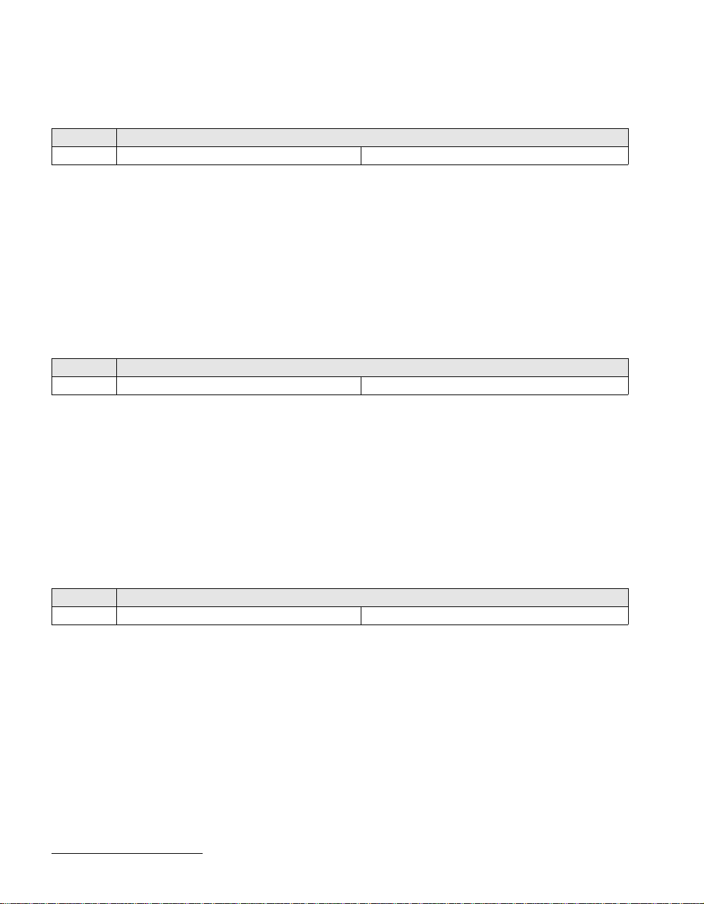
■ ML53301/ML53311 TC-622Pro/Pro+ ■ –––––––––––––––––––––––––––––––––––––––––––––––––––––––––––––
6.65 Receive Test Cell 2 Header Bytes 1 and 2 (default = 0x0000) Read/Write
Address 15 8 7 0
0x40 Receive Test Cell 2 Header Byte 1 Receive Test Cell 2 Header Byte 2
Receive Test Cell 2 Header byte 1 Bits 15:8
Contains header byte 1 of Test Cell Analyzer 2. The receive cell processor 2 detects a
test cell when it receives a cell with the user programmed header pattern.
The contents of this field are valid only in STS-12 mode and not in STS-12c mode.
Receive Test Cell 2 Header byte 2 Bits 7:0
Contains header byte 2 of Test Cell Analyzer 2. The receive cell processor 2 detects a
test cell when it receives a cell with the user programmed header pattern.
The contents of this field are valid only in STS-12 mode and not in STS-12c mode.
6.66 Receive Test Cell 1 Header Bytes 1 and 2 (default = 0x0000) Read/Write
Address 15 8 7 0
0x41 Receive Test Cell 1 Header Byte 1 Receive Test Cell 1 Header Byte 2
Receive Test Cell 1 Header byte 1 Bits 15:8
Contains header byte 1 of Test Cell Analyzer 1. The receive cell processor 1 detects a
test cell when it receives a cell with the user programmed header pattern.
The contents of this field are valid only in STS-12 mode and not in STS-12c mode.
Receive Test Cell 1 Header byte 2 Bits 7:0
Contains header byte 2 of Test Cell Analyzer 1. The receive cell processor 1 detects a
test cell when it receives a cell with the user programmed header pattern.
The contents of this field are valid only in STS-12 mode and not in STS-12c mode.
6.67 Receive Test Cell 0 Header Bytes 1 and 2 (default = 0x0000) Read/Write
Address 15 8 7 0
0x42 Receive Test Cell 0 Header Byte 1 Receive Test Cell 0 Header Byte 2
Receive Test Cell 1 Header byte 1 Bits 15:8
Contains header byte 1 of Test Cell Analyzer 0. The receive cell processor 0 detects a
test cell when it receives a cell with the user programmed header pattern.
The contents of this field are valid in both STS-12 mode and STS-12c mode.
Receive Test Cell 1 Header byte 2 Bits 7:0
Contains header byte 2 of Test Cell Analyzer 0. The receive cell processor 0 detects a
test cell when it receives a cell with the user programmed header pattern.
The contents of this field are valid in both STS-12 mode and STS-12c mode.
52 Oki Semiconductor
Page 59
––––––––––––––––––––––––––––––––––––––––––––––––––––––––––––– ■ ML53301/ML53311 TC-622Pro/Pro+ ■
6.68 Receive Test Cell 3 Header Bytes 3 and 4 (default = 0x0000) Read/Write
Address 15 8 7 0
0x43 Receive Test Cell 3 Header Byte 3 Receive Test Cell 3 Header Byte 4
Receive Test Cell 3 Header byte 3 Bits 15:8
Contains header byte 3 of Test Cell Analyzer 3. The receive cell processor 3 detects a
test cell when it receives a cell with the user programmed header pattern.
The contents of this field are valid only in STS-12 mode and not in STS-12c mode.
Receive Test Cell 3 Header byte 4 Bits 7:0
Contains header byte 4 of Test Cell Analyzer 3. The receive cell processor 3 detects a
test cell when it receives a cell with the user programmed header pattern.
The contents of this field are valid only in STS-12 mode and not in STS-12c mode.
6.69 Receive Test Cell 2 Header Bytes 3 and 4 (default = 0x0000) Read/Write
Address 15 8 7 0
0x44 Receive Test Cell 2 Header Byte 3 Receive Test Cell 2 Header Byte 4
Receive Test Cell 2 Header byte 3 Bits 15:8
Contains header byte 3 of Test Cell Analyzer 2. The receive cell processor 2 detects a
test cell when it receives a cell with the user programmed header pattern.
The contents of this field are valid only in STS-12 mode and not in STS-12c mode.
Receive Test Cell 2 Header byte 4 Bits 7:0
Contains header byte 4 of Test Cell Analyzer 2. The receive cell processor 2 detects a
test cell when it receives a cell with the user programmed header pattern.
The contents of this field are valid only in STS-12 mode and not in STS-12c mode.
6.70 Receive Test Cell 1 Header Bytes 3 and 4 (default = 0x0000) Read/Write
Address 15 8 7 0
0x45 Receive Test Cell 1 Header Byte 3 Receive Test Cell 1 Header Byte 4
Receive Test Cell 1 Header byte 3 Bits 15:8
Contains header byte 3 of Test Cell Analyzer 1. The receive cell processor 1 detects a
test cell when it receives a cell with the user programmed header pattern.
The contents of this field are valid only in STS-12 mode and not in STS-12c mode.
Receive Test Cell 1 Header byte 4 Bits 7:0
Contains header byte 4 of Test Cell Analyzer 1. The receive cell processor 1 detects a
test cell when it receives a cell with the user programmed header pattern.
The contents of this field are valid only in STS-12 mode and not in STS-12c mode.
53Oki Semiconductor
Page 60

■ ML53301/ML53311 TC-622Pro/Pro+ ■ –––––––––––––––––––––––––––––––––––––––––––––––––––––––––––––
6.71 Receive Test Cell 0 Header Bytes 3 and 4 (default = 0x0000) Read/Write
Address 15 8 7 0
0x46 Receive Test Cell 0 Header Byte 3 Receive Test Cell 0 Header Byte 4
Receive Test Cell 0 Header byte 3 Bits 15:8
Contains header byte 3 of Test Cell Analyzer 0. The receive cell processor 0 detects a
test cell when it receives a cell with the user programmed header pattern.
The contents of this field are valid in both STS-12 mode and STS-12c mode.
Receive Test Cell 0 Header byte 4 Bits 7:0
Contains header byte 4 of Test Cell Analyzer 0. The receive cell processor 0 detects a
test cell when it receives a cell with the user programmed header pattern.
The contents of this field are valid in both STS-12 mode and STS-12c mode.
6.72 User Commands To UTOPIA (default = 0x0000) Read/Write
Address 15 8 7 6 5 4 3 2 1 0
0x47 Unused C3 C2 C1 C0 E3 E2 E1 E0
C3 UTOPIA 3 Cell Bit 7
Setting this bit places UTOPIA 3 in 52-byte mode. Clearing the bit places the UTOPIA
3 in 54-byte mode.
This bit is valid only in STS12 mode and not in STS12c mode.
C2 UTOPIA 2 Cell Bit 6
Setting this bit places UTOPIA 2 in 52-byte mode. Clearing the bit places the UTOPIA
2 in 54-byte mode.
This bit is valid only in STS12 mode and not in STS12c mode.
C1 UTOPIA 1 Cell Bit 5
Setting this bit places UTOPIA 1 in 52-byte mode. Clearing the bit places the UTOPIA
1 in 54-byte mode.
This bit is valid only in STS12 mode and not in STS12c mode.
C0 UTOPIA 0 Cell Bit 4
Setting this bit places UTOPIA 0 in 52-byte mode. Clearing the bit places the UTOPIA
0 in 54-byte mode.
This bit is valid in both STS12 mode and STS12c mode.
E3 UTOPIA Error 3 Cell Bit 3
If this bit is set, transmit UTOPIA 3 drops a cell on parity error in incoming cell data
from the master UTOPIA.
This bit is valid only in STS12 mode and not in STS12c mode.
E2 UTOPIA Error 2 Cell Bit 2
If this bit is set, transmit UTOPIA 2 drops a cell on parity error in incoming cell data
from the master UTOPIA.
This bit is valid only in STS12 mode and not in STS12c mode.
E1 UTOPIA Error 1 Cell Bit 1
If this bit is set, transmit UTOPIA 1 drops a cell on parity error in incoming cell data
from the master UTOPIA.
This bit is valid only in STS12 mode and not in STS12c mode.
54 Oki Semiconductor
Page 61
––––––––––––––––––––––––––––––––––––––––––––––––––––––––––––– ■ ML53301/ML53311 TC-622Pro/Pro+ ■
E0 UTOPIA Error 0 Cell Bit 0
If this bit is set, transmit UTOPIA 0 drops a cell on parity error in incoming cell data
from the master UTOPIA.
This bit is valid in both STS12 mode and STS12c mode.
6.73 UTOPIA 3 Address Register (default = 0x0063) Read/Write
Address 15 10 9 5 4 0
0x48 Unused TxAddr3 RxAddr3
TxAddr3 UTOPIA 3 Transmit Address [9:5] Bits 9:5
Contains the 5 bit UTOPIA 3 Transmit Address. Default for this field 0x03.
RxAddr3 UTOPIA 3 Receive Address [4:0] Bits 4:0
Contains the 5 bit UTOPIA 3 Receive Address. Default for this field 0x03.
The contents of this register are valid only in STS12 mode and not in STS12c mode.
6.74 UTOPIA 2 Address Register (default = 0x0042) Read/Write
Address 15 10 9 5 4 0
0x49 Unused TxAddr2 RxAddr2
TxAddr2 UTOPIA 2 Transmit Address [9:5] Bits 9:5
Contains the 5 bit UTOPIA 2 Transmit Address. Default for this field 0x02.
RxAddr2 UTOPIA 2 Receive Address [4:0] Bits 4:0
Contains the 5 bit UTOPIA 2 Receive Address. Default for this field 0x02.
The contents of this register are valid only in STS12 mode and not in STS12c mode.
6.75 UTOPIA 1 Address Register (default = 0x0021) Read/Write
Address 15 10 9 5 4 0
0x4A Unused TxAddr1 RxAddr1
TxAddr1 UTOPIA 1 Transmit Address [9:5] Bits 9:5
Contains the 5 bit UTOPIA 1 Transmit Address. Default for this field 0x01.
RxAddr1 UTOPIA 1 Receive Address [4:0] Bits 4:0
Contains the 5 bit UTOPIA 1 Receive Address. Default for this field 0x01.
The contents of this register are valid only in STS12 mode and not in STS12c mode.
55Oki Semiconductor
Page 62
■ ML53301/ML53311 TC-622Pro/Pro+ ■ –––––––––––––––––––––––––––––––––––––––––––––––––––––––––––––
6.76 UTOPIA 0 Address Register (default = 0x0000) Read/Write
Address 15 10 9 5 4 0
0x4B Unused TxAddr0 RxAddr0
TxAddr0 UTOPIA 0 Transmit Address [9:5] Bits 9:5
Contains the 5 bit UTOPIA 0 Transmit Address. Default for this field 0x00.
RxAddr0 UTOPIA 0 Receive Address [4:0] Bits 4:0
Contains the 5 bit UTOPIA 0 Receive Address. Default for this field 0x00.
The contents of this register are valid in both STS12 mode and STS12c mode.
6.77 TxUTOPIA FIFO Status Register (default = 0x0000) Read Only
Address 15 4 3 2 1 0
0x4C Unused U3TE U2TE U1TE U0TE
U3TE UTOPIA 3 Transmit Error Bit 3
This bit is set to indicate that a parity error has been detected on the incoming cell
data for UTOPIA 3.
This bit is valid only in STS12 mode and not in STS12c mode.
U2TE UTOPIA 2 Transmit Error Bit 2
This bit is set to indicate that a parity error has been detected on the incoming cell
data for UTOPIA 2.
This bit is valid only in STS12 mode and not in STS12c mode.
U1TE UTOPIA 1 Transmit Error Bit 1
This bit is set to indicate that a parity error has been detected on the incoming cell
data for UTOPIA 1.
This bit is valid only in STS12 mode and not in STS12c mode.
U0TE UTOPIA 0 Transmit Error Bit 0
This bit is set to indicate that a parity error has been detected on the incoming cell
data for UTOPIA 0.
This bit is valid in both STS12 mode and STS12c mode.
6.78 TxUTOPIA Cell Drop Status Register (default = 0x0000) Read Only
Address 15 8 7 6 5 4 3 2 1 0
0x4D Unused U3CA U2CA U1CA U0CA U3PE U2PE U1PE U0PE
U3CA UTOPIA 3 Change of Cell Alignment Bit 7
This bit is set when the UTOPIA 3 port has a change of cell alignment.
This bit is valid only in STS12 mode and not in STS12c mode.
U2CA UTOPIA 2 Change of Cell Alignment Bit 6
This bit is set when the UTOPIA 2 port has a change of cell alignment.
This bit is valid only in STS12 mode and not in STS12c mode.
56 Oki Semiconductor
Page 63
––––––––––––––––––––––––––––––––––––––––––––––––––––––––––––– ■ ML53301/ML53311 TC-622Pro/Pro+ ■
U1CA UTOPIA 1 Change of Cell Alignment Bit 5
This bit is set when the UTOPIA 1 port has a change of cell alignment.
This bit is valid only in STS12 mode and not in STS12c mode.
U0CA UTOPIA 0 Change of Cell Alignment Bit 4
This bit is set when the UTOPIA 0 port has a change of cell alignment.
This bit is valid in both STS12 mode and STS12c mode.
U3PE UTOPIA 3 Transmit Parity Error Cell Dropped Bit 3
This bit is set when the UTOPIA 3 port has dropped a transmit parity error cell.
This bit is valid only in STS12 mode and not in STS12c mode.
U2PE UTOPIA 2 Transmit Parity Error Cell Dropped Bit 2
This bit is set when the UTOPIA 2 port has dropped a transmit parity error cell.
This bit is valid only in STS12 mode and not in STS12c mode.
U1PE UTOPIA 1 Transmit Parity Error Cell Dropped Bit 1
This bit is set when the UTOPIA 1 port has dropped a transmit parity error cell.
This bit is valid only in STS12 mode and not in STS12c mode.
U0PE UTOPIA 0 Transmit Parity Error Cell Dropped Bit 0
This bit is set when the UTOPIA 0 port has dropped a transmit parity error cell.
This bit is valid in both STS12 mode and STS12c mode.
Reserved For Future Use (default = 0x0000) Read Only
Address 15 0
0x4E Unused
6.79 Receive Cell Processor User Commands (default = 0x000F) Read/Write
Address 15 8 7 6 5 4 3 2 1 0
0x4F Unused LCD3 LCD2 LCD1 LCD0 HEC3 HEC2 HEC1 HEC0
LCD3 Loss of Cell Delineation_3 Bit 7
This bit is checked by receive cell processor 3 in the LCD_Defect_Verify state. The user
should monitor the LCD defect period and set this bit at the appropriate time if necessary. If an LCD failure is declared, the cell processor does not come out of the
LCD_Defect_Verify state, even if it is receiving proper HEC bytes, unless the LCD failure is reset.
This bit is only valid in STS-12 mode and not in STS-12c mode.
LCD2 Loss of Cell Delineation_2 Bit 6
This bit is checked by receive cell processor 2 in the LCD_Defect_Verify state. The user
should monitor the LCD defect period and set this bit at the appropriate time if necessary. If an LCD failure is declared, the cell processor does not come out of the
LCD_Defect_Verify state, even if it is receiving proper HEC bytes, unless the LCD failure is reset.
This bit is only valid in STS-12 mode and not in STS-12c mode.
57Oki Semiconductor
Page 64

■ ML53301/ML53311 TC-622Pro/Pro+ ■ –––––––––––––––––––––––––––––––––––––––––––––––––––––––––––––
LCD1 Loss of Cell Delineation_1 Bit 5
This bit is checked by receive cell processor 1 in the LCD_Defect_Verify state. The user
should monitor the LCD defect period and set this bit at the appropriate time if necessary. If an LCD failure is declared, the cell processor does not come out of the
LCD_Defect_Verify state, even if it is receiving proper HEC bytes, unless the LCD failure is reset.
This bit is only valid in STS-12 mode and not in STS-12c mode.
LCD0 Loss of Cell Delineation_0 Bit 4
This bit is checked by receive cell processor 0 in the LCD_Defect_Verify state. The user
should monitor the LCD defect period and set this bit at the appropriate time if necessary. If an LCD failure is declared, the cell processor does not come out of the
LCD_Defect_Verify state, even if it is receiving proper HEC bytes, unless the LCD failure is reset.
This bit is valid in both STS-12 mode and STS-12c mode.
HEC3 Header Error Correction Enable_3 Bit 3
This bit is checked by receive cell processor 3 in the Sync_Correction state. If this bit is
set, single-bit header errors are corrected and given out. If the HEC3 bit is cleared,
cells with single-bit errors are discarded.
This bit is only valid in STS-12 mode and not in STS-12c mode.
HEC2 Header Error Correction Enable_2 Bit 2
This bit is checked by receive cell processor 2 in the Sync_Correction state. If this bit is
set, single-bit header errors are corrected and given out. If the HEC2 bit is cleared,
cells with single-bit errors are discarded.
This bit is only valid in STS-12 mode and not in STS-12c mode.
HEC1 Header Error Correction Enable_1 Bit 1
This bit is checked by receive cell processor 1 in the Sync_Correction state. If this bit is
set, single-bit header errors are corrected and given out. If the HEC1 bit is cleared,
cells with single-bit errors are discarded.
This bit is only valid in STS-12 mode and not in STS-12c mode.
HEC0 Header Error Correction Enable_0 Bit 0
This bit is checked by receive cell processor 0 in the Sync_Correction state. If this bit is
set, single-bit header errors are corrected and given out. If the HEC0 bit is cleared,
cells with single-bit errors are discarded.
This bit is valid in both STS-12 mode and STS-12c mode.
6.80 Transmit Framer User Commands (default = 0x0000) Read/Write
Address 15 10 9 8 7 6 5 4 3 2 1 0
0x50 Unused PAIS3 PAIS2 PAIS1 PAIS0 PRDI3 PRDI2 PRDI1 PRDI0 LAIS LRDI
PAIS3 Path Alarm Indication Signal_3 Bit 9
When the PAIS3 bit is set, a pattern of all ones is transmitted over Synchronous Payload Envelope 3 (SPE3) and its corresponding pointer bytes. The transmission of all
ones occurs as soon as the transmit framer receives the command.
This bit is only valid in STS-12 mode and not in STS-12c mode.
58 Oki Semiconductor
Page 65

––––––––––––––––––––––––––––––––––––––––––––––––––––––––––––– ■ ML53301/ML53311 TC-622Pro/Pro+ ■
PAIS2 Path Alarm Indication Signal_2 Bit 8
When the PAIS2 bit is set, a pattern of all ones is transmitted over Synchronous Payload Envelope 2 (SPE2) and its corresponding pointer bytes. The transmission of all
ones occurs as soon as the transmit framer receives the command.
This bit is only valid in STS-12 mode and not in STS-12c mode.
PAIS1 Path Alarm Indication Signal_1 Bit 7
When the PAIS1 bit is set, a pattern of all ones is transmitted over Synchronous Payload Envelope 1 (SPE1) and its corresponding pointer bytes. The transmission of all
ones occurs as soon as the transmit framer receives the command.
This bit is only valid in STS-12 mode and not in STS-12c mode.
PAIS0 Path Alarm Indication Signal_0 Bit 6
When the PAIS0 bit is set, a pattern of all ones is transmitted over Synchronous Payload Envelope 0 (SPE0) and its corresponding pointer bytes. The transmission of all
ones occurs as soon as the transmit framer receives the command.
This bit is valid in both STS-12 mode and STS-12c mode.
PRDI3 Path Remote Defect Indication_3 Bit 5
When the PRDI3 bit is set, a Path Remote Defect Indication is transmitted in Synchronous Payload Envelope 3 (SPE3). The G1 byte in the path overhead (POH) has one
bit reserved for P-RDI transmission. The P-RDI indication is transmitted once per
frame. The transmit framer checks this bit just before the G1 location.
This bit is only valid in STS-12 mode and not in STS-12c mode.
PRDI2 Path Remote Defect Indication_2 Bit 4
When the PRDI2 bit is set, a Path Remote Defect Indication is transmitted in Synchronous Payload Envelope 2 (SPE2). The G1 byte in the path overhead (POH) has one
bit reserved for P-RDI transmission. The P-RDI indication is transmitted once per
frame. The transmit framer checks this bit just before the G1 location.
This bit is only valid in STS-12 mode and not in STS-12c mode.
PRDI1 Path Remote Defect Indication_1 Bit 3
When the PRDI1 bit is set, a Path Remote Defect Indication is transmitted in Synchronous Payload Envelope 1 (SPE1). The G1 byte in the path overhead (POH) has one
bit reserved for P-RDI transmission. The P-RDI indication is transmitted once per
frame. The transmit framer checks this bit just before the G1 location.
This bit is only valid in STS-12 mode and not in STS-12c mode.
PRDI0 Path Remote Defect Indication_0 Bit 2
When the PRDI0 bit is set, a Path Remote Defect Indication is transmitted in Synchronous Payload Envelope 0 (SPE3). The G1 byte in the path overhead (POH) has one
bit reserved for P-RDI transmission. The P-RDI indication is transmitted once per
frame. The transmit framer checks this bit just before the G1 location.
This bit is valid in both STS-12 mode and STS-12c mode.
LAIS Line Alarm Indication Signal Bit 1
The K2 byte in the line overhead (LOH) of each frame has three bits reserved for line
AIS transmission. When this bit is set, a value of 111b is transmitted on these bits in
the K2 byte. This indication is transmitted once per frame. The transmit framer
checks this bit just before the K2 location.
This bit is valid in both STS-12 mode and STS-12c mode.
LRDI Line Remote Defect Indication Bit 0
The K2 byte in the line overhead (LOH) of each frame has three bits reserved for line
RDI transmission. When this bit is set, a value of 110b is transmitted on these bits in
59Oki Semiconductor
Page 66

■ ML53301/ML53311 TC-622Pro/Pro+ ■ –––––––––––––––––––––––––––––––––––––––––––––––––––––––––––––
the K2 byte. This indication is transmitted once per frame. The transmit framer
checks this bit just before the K2 location.
This bit is valid in both STS-12 mode and STS-12c mode.
6.81 Transmit Cell Processor User Commands (default = 0x00F0) Read/Write
Address 15 8 7 6 5 4 3 2 1 0
0x51 Unused GFC3 GFC2 GFC1 GFC0 TCE3 TCE2 TCE1 TCE0
GFC3 Generic Flow Control Enable_3 Bit 7
This bit is used for flow control by transmit cell processor 3. If this bit is set, and if
there is GFC feedback from receive cell processor 3, an assigned cell is not read from
transmit UTOPIA buffer 3, even if a cell is available. Transmit cell processor 3 continues sending idle cells (or test cells if they are enabled) if there is GFC feedback
from receive cell processor 3. If this bit is cleared, receive flow control is disabled.
This bit is only valid in STS-12 mode and not in STS-12c mode.
GFC2 Generic Flow Control Enable_2 Bit 6
This bit is used for flow control by transmit cell processor 2. If this bit is set, and if
there is GFC feedback from receive cell processor 2, an assigned cell is not read from
transmit UTOPIA buffer 2, even if a cell is available. Transmit cell processor 2 continues sending idle cells (or test cells if they are enabled) if there is GFC feedback
from receive cell processor 2. If this bit is cleared, then receive flow control is disabled.
This bit is only valid in STS-12 mode and not in STS-12c mode.
GFC1 Generic Flow Control Enable_1 Bit 5
This bit is used for flow control by transmit cell processor 1. If this bit is set, and if
there is GFC feedback from receive cell processor 1, an assigned cell is not read from
transmit UTOPIA buffer 1, even if a cell is available. Transmit cell processor 1 continues sending idle cells (or test cells if they are enabled) if there is GFC feedback
from receive cell processor 1. If this bit is cleared, then receive flow control is disabled.
This bit is only valid in STS-12 mode and not in STS-12c mode.
GFC0 Generic Flow Control Enable_0 Bit 4
This bit is used for flow control by transmit cell processor 0. If this bit is set, and if
there is GFC feedback from receive cell processor 0, an assigned cell is not read from
transmit UTOPIA buffer 0, even if a cell is available. Transmit cell processor 0 continues sending idle cells (or test cells if they are enabled) if there is GFC feedback
from receive cell processor 0.
This bit is valid in both STS-12 mode and STS-12c mode.
TCE3 Test Cell Enable_3 Bit 3
This bit is used by transmit cell processor 3 to determine which cells (test or idle) to
use for cell rate adaptation. If this bit is set, the cell processor transmits the test cells
generated by test cell generator 3 whenever there are no assigned cells to transmit. If
the bit is cleared, normal idle cells are used for cell rate adaptation.
This bit is only valid in STS-12 mode and not in STS-12c mode.
TCE2 Test Cell Enable_2 Bit 2
This bit is used by transmit cell processor 2 to determine which cells (test or idle) to
use for cell rate adaptation. If this bit is set, the cell processor transmits the test cells
60 Oki Semiconductor
Page 67

––––––––––––––––––––––––––––––––––––––––––––––––––––––––––––– ■ ML53301/ML53311 TC-622Pro/Pro+ ■
generated by test cell generator 2 whenever there are no assigned cells to transmit. If
the bit is cleared, normal idle cells are used for cell rate adaptation.
This bit is only valid in STS-12 mode and not in STS-12c mode.
TCE1 Test Cell Enable_1 Bit 1
This bit is used by transmit cell processor 1 to determine which cells (test or idle) to
use for cell rate adaptation. If this bit is set, the cell processor transmits the test cells
generated by test cell generator 1 whenever there are no assigned cells to transmit. If
the bit is cleared, normal idle cells are used for cell rate adaptation.
This bit is only valid in STS-12 mode and not in STS-12c mode.
TCE0 Test Cell Enable_0 Bit 0
This bit is used by transmit cell processor 0 to determine which cells (test or idle) to
use for cell rate adaptation. If this bit is set, the cell processor transmits the test cells
generated by test cell generator 0 whenever there are no assigned cells to transmit. If
the bit is cleared, normal idle cells are used for cell rate adaptation.
This bit is valid in both STS-12 mode and STS-12c mode.
6.82 Parity Error Roll-Over (default = 0x0000) Read/Write/Set
Address 15 10 9 8 7 6 5 4 3 2 1 0
0x52 Unused TC3ER TC2ER TC1ER TC0ER SPE3 SPE2 SPE1 SPE0 B2ERR B1ERR
TC3ER Test Cell Analyzer 3 Error Count Bit 9
This bit provides a roll-over indication for the test cell analyzer 3 error count register
located at address 0x07. When a roll-over occurs this bit is set and the user must explicitly reset it after reading it.
This bit is only valid in STS-12 mode and not in STS-12c mode.
TC2ER Test Cell Analyzer 2 Error Count Bit 8
This bit provides a roll-over indication for the test cell analyzer 2 error count register
located at address 0x08. When a roll-over occurs this bit is set and the user must explicitly reset it after reading it.
This bit is only valid in STS-12 mode and not in STS-12c mode.
TC1ER Test Cell Analyzer 1 Error Count Bit 7
This bit provides a roll-over indication for the test cell analyzer 1 error count register
located at address 0x09. When a roll-over occurs this bit is set and the user must explicitly reset it after reading it.
This bit is only valid in STS-12 mode and not in STS-12c mode.
TC0ER Test Cell Analyzer 0 Error Count Bit 6
This bit provides a roll-over indication for the test cell analyzer 0 error count register
located at address 0x0A. When a roll-over occurs this bit is set and the user must explicitly reset it after reading it.
This bit is valid in both STS-12 mode and STS-12c mode.
SPE3 B3 Parity Error Count for SPE3 Bit 5
This bit provides a roll-over indication of the receive B3 parity error count for SPE3.
This register is located at address 0x03. When a roll-over occurs this bit is set and the
user must explicitly reset it after reading it.
This bit is only valid in STS-12 mode and not in STS-12c mode.
61Oki Semiconductor
Page 68

■ ML53301/ML53311 TC-622Pro/Pro+ ■ –––––––––––––––––––––––––––––––––––––––––––––––––––––––––––––
SPE2 B3 Parity Error Count for SPE2 Bit 4
This bit provides a roll-over indication of the receive B3 parity error count for SPE2.
This register is located at address 0x04. When a roll-over occurs this bit is set and the
user must explicitly reset it after reading it.
This bit is only valid in STS-12 mode and not in STS-12c mode.
SPE1 B3 Parity Error Count for SPE1 Bit 3
This bit provides a roll-over indication of the receive B3 parity error count for SPE1.
This register is located at address 0x05. When a roll-over occurs this bit is set and the
user must explicitly reset it after reading it.
This bit is only valid in STS-12 mode and not in STS-12c mode.
SPE0 B3 Parity Error Count for SPE0 Bit 2
This bit provides a roll-over indication of the receive B3 parity error count for SPE0.
This register is located at address 0x06. When a roll-over occurs this bit is set and the
user must explicitly reset it after reading it.
This bit is valid in both STS-12 mode and STS-12c mode.
B2ERR B2 Parity Error Count Bit 1
This bit provides a roll-over indication of the receive B2 parity error count register
located at address 0x02. When a roll-over occurs this bit is set and the user must explicitly reset it after reading it.
This bit is valid in both STS-12 mode and STS-12c mode.
B1ERR B1 Parity Error Count Bit 0
This bit provides a roll-over indication of the receive B2 parity error count register
located at address 0x01. When a roll-over occurs this bit is set and the user must explicitly reset it after reading it.
This bit is valid in both STS-12 mode and STS-12c mode.
6.83 Receiver Alarm Roll-Over (default = 0x0000) Read/Write/Set
Address 15 13 12 11 10 9 8 7 6 5 4 3 2 1 0
0x53 Unused SLM3 SLM2 SLM1 SLM0 PA3 PA2 PA1 PA0 CD3 CD2 CD1 CD0 LRO
SLM3 Signal Label Mismatch_3 Bit 12
This bit provides a roll-over indication of the receive signal label mismatch count for
SPE3. This register is located at address 0x2C. When a roll-over occurs this bit is set
and the user must explicitly reset it after reading it.
This bit is only valid in STS-12 mode and not in STS-12c mode.
SLM2 Signal Label Mismatch_2 Bit 11
This bit provides a roll-over indication of the receive signal label mismatch count for
SPE2. This register is located at address 0x2D. When a roll-over occurs this bit is set
and the user must explicitly reset it after reading it.
This bit is only valid in STS-12 mode and not in STS-12c mode.
SLM1 Signal Label Mismatch_1 Bit 10
This bit provides a roll-over indication of the receive signal label mismatch count for
SPE1. This register is located at address 0x2E. When a roll-over occurs this bit is set
and the user must explicitly reset it after reading it.
This bit is only valid in STS-12 mode and not in STS-12c mode.
62 Oki Semiconductor
Page 69

––––––––––––––––––––––––––––––––––––––––––––––––––––––––––––– ■ ML53301/ML53311 TC-622Pro/Pro+ ■
SLM0 Signal Label Mismatch_0 Bit 9
This bit provides a roll-over indication of the receive signal label mismatch count for
SPE0. This register is located at address 0x2F. When a roll-over occurs this bit is set
and the user must explicitly reset it after reading it.
This bit is valid in both STS-12 mode and STS-12c mode.
PA3 Path-FEBE Accumulator_3 Bit 8
This bit provides a roll-over indication of the receive path-FEBE (Far End Block Error) accumulator for SPE3. This register is located at address 0x0C. When a roll-over
occurs this bit is set and the user must explicitly reset it after reading it.
This bit is only valid in STS-12 mode and not in STS-12c mode.
PA2 Path-FEBE Accumulator_2 Bit 7
This bit provides a roll-over indication of the receive path-FEBE (Far End Block Error) accumulator for SPE2. This register is located at address 0x0D. When a roll-over
occurs this bit is set and the user must explicitly reset it after reading it.
This bit is only valid in STS-12 mode and not in STS-12c mode.
PA1 Path-FEBE Accumulator_1 Bit 6
This bit provides a roll-over indication of the receive path-FEBE (Far End Block Error) accumulator for SPE1. This register is located at address 0x0E. When a roll-over
occurs this bit is set and the user must explicitly reset it after reading it.
This bit is only valid in STS-12 mode and not in STS-12c mode.
PA0 Path-FEBE Accumulator_0 Bit 5
This bit provides a roll-over indication of the receive path-FEBE (Far End Block Error) accumulator for SPE0. This register is located at address 0x0F. When a roll-over
occurs this bit is set and the user must explicitly reset it after reading it.
This bit is valid in both STS-12 mode and STS-12c mode.
CD3 Cell Discard Count_3 Bit 4
This bit provides a roll-over indication of the receive cell processor 3 discard count
register located at address 0x28. When a roll-over occurs this bit is set and the user
must explicitly reset it after reading it.
This bit is only valid in STS-12 mode and not in STS-12c mode.
CD2 Cell Discard Count_2 Bit 3
This bit provides a roll-over indication of the receive cell processor 2 discard count
register located at address 0x29. When a roll-over occurs this bit is set and the user
must explicitly reset it after reading it.
This bit is only valid in STS-12 mode and not in STS-12c mode.
CD1 Cell Discard Count_1 Bit 2
This bit provides a roll-over indication of the receive cell processor 1 discard count
register located at address 0x2A. When a roll-over occurs this bit is set and the user
must explicitly reset it after reading it.
This bit is only valid in STS-12 mode and not in STS-12c mode.
CD0 Cell Discard Count_0 Bit 1
This bit provides a roll-over indication of the receive cell processor 0 discard count
register located at address 0x2B. When a roll-over occurs this bit is set and the user
must explicitly reset it after reading it.
This bit is valid in both STS-12 mode and STS-12c mode.
63Oki Semiconductor
Page 70

■ ML53301/ML53311 TC-622Pro/Pro+ ■ –––––––––––––––––––––––––––––––––––––––––––––––––––––––––––––
LRO Line-FEBE Roll-Over Bit 0
This bit provides a roll-over indication of the receive line-FEBE count register located
at address 0x0B. When a roll-over occurs this bit is set and the user must explicitly
reset it after reading it.
This bit is valid in both STS-12 mode and STS-12c mode.
6.84 Test Cell Count Roll-over (default = 0x0000) Read/Write/Set
Address 15 8 7 6 5 4 3 2 1 0
0x54 Unused TCG3 TCG2 TCG1 TCG0 TCA3 TCA2 TCA1 TCA0
TCG3 Test Cell Generator_3 Roll-over Bit 7
This bit provides a roll-over indication of the test cell generator 3 transmitted count
register located at address 0x10. When a roll-over occurs this bit is set and the user
must explicitly reset it after reading it.
This bit is only valid in STS-12 mode and not in STS-12c mode.
TCG2 Test Cell Generator_2 Roll-over Bit 6
This bit provides a roll-over indication of the test cell generator 2 transmitted count
register located at address 0x11. When a roll-over occurs this bit is set and the user
must explicitly reset it after reading it.
This bit is only valid in STS-12 mode and not in STS-12c mode.
TCG1 Test Cell Generator_1 Roll-over Bit 5
This bit provides a roll-over indication of the test cell generator 1 transmitted count
register located at address 0x12. When a roll-over occurs this bit is set and the user
must explicitly reset it after reading it.
This bit is only valid in STS-12 mode and not in STS-12c mode.
TCG0 Test Cell Generator_0 Roll-over Bit 4
This bit provides a roll-over indication of the test cell generator 0 transmitted count
register located at address 0x13. When a roll-over occurs this bit is set and the user
must explicitly reset it after reading it.
This bit is valid in both STS-12 mode and STS-12c mode.
TCA3 Test Cell Analyzer_3 Roll-over Bit 3
This bit provides a roll-over indication of the test cell analyzer 3 received count register located at address 0x14. When a roll-over occurs this bit is set and the user must
explicitly reset it after reading it.
This bit is only valid in STS-12 mode and not in STS-12c mode.
TCA2 Test Cell Analyzer_2 Roll-over Bit 2
This bit provides a roll-over indication of the test cell analyzer 2 received count register located at address 0x15. When a roll-over occurs this bit is set and the user must
explicitly reset it after reading it.
This bit is only valid in STS-12 mode and not in STS-12c mode.
TCA1 Test Cell Analyzer_1 Roll-over Bit 1
This bit provides a roll-over indication of the test cell analyzer 1 received count register located at address 0x16. When a roll-over occurs this bit is set and the user must
explicitly reset it after reading it.
This bit is only valid in STS-12 mode and not in STS-12c mode.
64 Oki Semiconductor
Page 71

––––––––––––––––––––––––––––––––––––––––––––––––––––––––––––– ■ ML53301/ML53311 TC-622Pro/Pro+ ■
TCA0 Test Cell Analyzer_0 Roll-over Bit 0
This bit provides a roll-over indication of the test cell analyzer 0 received count register located at address 0x17. When a roll-over occurs this bit is set and the user must
explicitly reset it after reading it.
This bit is valid in both STS-12 mode and STS-12c mode.
6.85 Transmit/Receive Count Roll-over (default = 0x0000) Read/Write/Set
Address 15 14 13 12 11 10 9 8 7 6 5 4 3 2 1 0
0x55 TA3 TA2 TA1 TA0 TU3 TU2 TU1 TU0 RA3 RA2 RA1 RA0 RU3 RU2 RU1 RU0
TA3 Transmit Cell Processor 3 Assigned Cell Count Bit 15
This bit provides a roll-over indication of the transmit cell processor 3 assigned cell
transmitted count register located at address 0x18. When a roll-over occurs this bit is
set and the user must explicitly reset it after reading it.
This bit is only valid in STS-12 mode and not in STS-12c mode.
TA2 Transmit Cell Processor 2 Assigned Cell Count Bit 14
This bit provides a roll-over indication of the transmit cell processor 2 assigned cell
transmitted count register located at address 0x19. When a roll-over occurs this bit is
set and the user must explicitly reset it after reading it.
This bit is only valid in STS-12 mode and not in STS-12c mode.
TA1 Transmit Cell Processor 1 Assigned Cell Count Bit 13
This bit provides a roll-over indication of the transmit cell processor 1 assigned cell
transmitted count register located at address 0x1A. When a roll-over occurs this bit
is set and the user must explicitly reset it after reading it.
This bit is only valid in STS-12 mode and not in STS-12c mode.
TA0 Transmit Cell Processor 0 Assigned Cell Count Bit 12
This bit provides a roll-over indication of the transmit cell processor 0 assigned cell
transmitted count register located at address 0x1B. When a roll-over occurs this bit is
set and the user must explicitly reset it after reading it.
This bit is valid in both STS-12 mode and STS-12c mode.
TU3 Transmit Cell Processor 3 Idle Cell Count Bit 11
This bit provides a roll-over indication of the transmit cell processor 3 idle cell transmitted count register located at address 0x1C. When a roll-over occurs this bit is set
and the user must explicitly reset it after reading it.
This bit is only valid in STS-12 mode and not in STS-12c mode.
TU2 Transmit Cell Processor 2 Idle Cell Count Bit 10
This bit provides a roll-over indication of the transmit cell processor 2 idle cell transmitted count register located at address 0x1D. When a roll-over occurs this bit is set
and the user must explicitly reset it after reading it.
This bit is only valid in STS-12 mode and not in STS-12c mode.
TU1 Transmit Cell Processor 1 Idle Cell Count Bit 9
This bit provides a roll-over indication of the transmit cell processor 1 idle cell transmitted count register located at address 0x1E. When a roll-over occurs this bit is set
and the user must explicitly reset it after reading it.
This bit is only valid in STS-12 mode and not in STS-12c mode.
65Oki Semiconductor
Page 72

■ ML53301/ML53311 TC-622Pro/Pro+ ■ –––––––––––––––––––––––––––––––––––––––––––––––––––––––––––––
TU0 Transmit Cell Processor 0 Idle Cell Count Bit 8
This bit provides a roll-over indication of the transmit cell processor 0 idle cell transmitted count register located at address 0x1F. When a roll-over occurs this bit is set
and the user must explicitly reset it after reading it.
This bit is valid in both STS-12 mode and STS-12c mode.
RA3 Receive Cell Processor 3 Assigned Cell Count Bit 7
This bit provides a roll-over indication of the receive cell processor 3 assigned cell received count register located at address 0x20. When a roll-over occurs this bit is set
and the user must explicitly reset it after reading it.
This bit is only valid in STS-12 mode and not in STS-12c mode.
RA2 Receive Cell Processor 2 Assigned Cell Count Bit 6
This bit provides a roll-over indication of the receive cell processor 2 assigned cell received count register located at address 0x21. When a roll-over occurs this bit is set
and the user must explicitly reset it after reading it.
This bit is only valid in STS-12 mode and not in STS-12c mode.
RA1 Receive Cell Processor 1 Assigned Cell Count Bit 5
This bit provides a roll-over indication of the receive cell processor 1 assigned cell received count register located at address 0x22. When a roll-over occurs this bit is set
and the user must explicitly reset it after reading it.
This bit is only valid in STS-12 mode and not in STS-12c mode.
RA0 Receive Cell Processor 0 Assigned Cell Count Bit 4
This bit provides a roll-over indication of the receive cell processor 0 assigned cell received count register located at address 0x23. When a roll-over occurs this bit is set
and the user must explicitly reset it after reading it.
This bit is valid in both STS-12 mode and STS-12c mode.
RU3 Receive Cell Processor 3 Idle Cell Count Bit 3
This bit provides a roll-over indication of the receive cell processor 3 idle cell received count register located at address 0x24. When a roll-over occurs this bit is set
and the user must explicitly reset it after reading it.
This bit is only valid in STS-12 mode and not in STS-12c mode.
RU2 Receive Cell Processor 2 Idle Cell Count Bit 2
This bit provides a roll-over indication of the receive cell processor 2 idle cell received count register located at address 0x25. When a roll-over occurs this bit is set
and the user must explicitly reset it after reading it.
This bit is only valid in STS-12 mode and not in STS-12c mode.
RU1 Receive Cell Processor 1 Idle Cell Count Bit 1
This bit provides a roll-over indication of the receive cell processor 1 idle cell received count register located at address 0x26. When a roll-over occurs this bit is set
and the user must explicitly reset it after reading it.
This bit is only valid in STS-12 mode and not in STS-12c mode.
RU0 Receive Cell Processor 0 Idle Cell Count Bit 0
This bit provides a roll-over indication of the receive cell processor 0 idle cell received count register located at address 0x27. When a roll-over occurs this bit is set
and the user must explicitly reset it after reading it.
This bit is valid in both STS-12 mode and STS-12c mode.
66 Oki Semiconductor
Page 73

––––––––––––––––––––––––––––––––––––––––––––––––––––––––––––– ■ ML53301/ML53311 TC-622Pro/Pro+ ■
6.86 Interrupt Mask Register (default = 0x0000) Read/Write
Address 31 16 15 14 13 12 11 10 9 8 7 6 5 4 3 2 1 0
0x56 Unused APE DPE R3O R2O R1O R0O LRIE LSIE L3RI L2RI L1RI L0RI L3SI L2SI L1SI L0SI
APE Address Parity Error Enable Bit 15
Setting this bit enables interrupts on address parity errors. Clearing the bit masks this
interrupt. Note that APE is a PCI bit specific to the ML53301 TC-622Pro.
This bit is valid in both STS12 mode and STS12c mode.
DPE Data Parity Error Enable Bit 14
Setting this bit enables interrupts on data parity errors. Clearing the bit masks this
interrupt. Note that DPE is a PCI bit specific to the ML53301 TC-622Pro.
This bit is valid in both STS12 mode and STS12c mode.
R3O Receive UTOPIA 3 Overrun Enable Bit 13
Setting this bit allows an interrupt to be generated when the receive UTOPIA 3 port
FIFO is overrun. Clearing the bit masks this interrupt.
This bit is only valid in STS12 mode and not in STS12c mode.
R2O Receive UTOPIA 2 Overrun Enable Bit 12
Setting this bit allows an interrupt to be generated when the receive UTOPIA 2 port
FIFO is overrun. Clearing the bit masks this interrupt.
This bit is only valid in STS12 mode and not in STS12c mode.
R1O Receive UTOPIA 1 Overrun Enable Bit 11
Setting this bit allows an interrupt to be generated when the receive UTOPIA 1 port
FIFO is overrun. Clearing the bit masks this interrupt.
This bit is only valid in STS12 mode and not in STS12c mode.
R0O Receive UTOPIA 0 Overrun Enable Bit 10
Setting this bit allows an interrupt to be generated when the receive UTOPIA 0 port
FIFO is overrun. Clearing the bit masks this interrupt.
This bit is valid in both STS12 mode and STS12c mode.
LRIE Loss of Frame Reset Interrupt Enable Bit 9
Setting this bit allows an interrupt to be generated when the Loss of Frame (LOF)
state machine enters the reset state. Clearing the bit masks this interrupt.
This bit is valid in both STS12 mode and STS12c mode.
LSIE Loss of Frame Set Interrupt Enable Bit 8
Setting this bit allows an interrupt to be generated when the Loss of Frame (LOF)
state machine enters the set state. Clearing the bit masks this interrupt.
This bit is valid in both STS12 mode and STS12c mode.
L3RI Loss of Cell Delineation 3 Reset Interrupt Enable Bit 7
Setting this bit allows an interrupt to be generated when the Loss of Cell Delineation
(LCD) state machine for cell processor 3 enters the reset state. Clearing the bit masks
this interrupt.
This bit is only valid in STS12 mode and not in STS12c mode.
L2RI Loss of Cell Delineation 2 Reset Interrupt Enable Bit 6
Setting this bit allows an interrupt to be generated when the Loss of Cell Delineation
(LCD) state machine for cell processor 2 enters the reset state. Clearing the bit masks
67Oki Semiconductor
Page 74

■ ML53301/ML53311 TC-622Pro/Pro+ ■ –––––––––––––––––––––––––––––––––––––––––––––––––––––––––––––
this interrupt.
This bit is only valid in STS12 mode and not in STS12c mode.
L1RI Loss of Cell Delineation 1 Reset Interrupt Enable Bit 5
Setting this bit allows an interrupt to be generated when the Loss of Cell Delineation
(LCD) state machine for cell processor 1 enters the reset state. Clearing the bit masks
this interrupt.
This bit is only valid in STS12 mode and not in STS12c mode.
L0RI Loss of Cell Delineation 0 Reset Interrupt Enable Bit 4
Setting this bit allows an interrupt to be generated when the Loss of Cell Delineation
(LCD) state machine for cell processor 0 enters the reset state. Clearing the bit masks
this interrupt.
This bit is valid in both STS12 mode and STS12c mode.
L3SI Loss of Cell Delineation 3 Set Interrupt Enable Bit 3
Setting this bit allows an interrupt to be generated when the Loss of Cell Delineation
(LCD) state machine for cell processor 3 enters the set state. Clearing the bit masks
this interrupt.
This bit is only valid in STS12 mode and not in STS12c mode.
L2SI Loss of Cell Delineation 2 Set Interrupt Enable Bit 2
Setting this bit allows an interrupt to be generated when the Loss of Cell Delineation
(LCD) state machine for cell processor 2 enters the set state. Clearing the bit masks
this interrupt.
This bit is only valid in STS12 mode and not in STS12c mode.
L1SI Loss of Cell Delineation 1 Set Interrupt Enable Bit 1
Setting this bit allows an interrupt to be generated when the Loss of Cell Delineation
(LCD) state machine for cell processor 1 enters the set state. Clearing the bit masks
this interrupt.
This bit is only valid in STS12 mode and not in STS12c mode.
L0SI Loss of Cell Delineation 0 Set Interrupt Enable Bit 0
Setting this bit allows an interrupt to be generated when the Loss of Cell Delineation
(LCD) state machine for cell processor 0 enters the set state. Clearing the bit masks
this interrupt.
This bit is valid in both STS12 mode and STS12c mode.
6.87 Interrupt Status Register (default = 0x0000) Read/Write
Address 31 16 15 14 13 12 11 10 9 8 7 6 5 4 3 2 1 0
0x57 Unused APE DPE R3O R2O R1O R0O LRIE LSIE L3RI L2RI L1RI L0RI L3SI L2SI L1SI L0SI
APE Address Parity Error Bit 15
This bit is set on a PCI address parity error if bit 15 of the Interrupt Mask Register is
set.
This bit is valid in both STS12 mode and STS12c mode.
DPE Data Parity Error Bit 14
This bit is set on a PCI data parity error if bit 14 of the Interrupt Mask Register is set.
This bit is valid in both STS12 mode and STS12c mode.
68 Oki Semiconductor
Page 75

––––––––––––––––––––––––––––––––––––––––––––––––––––––––––––– ■ ML53301/ML53311 TC-622Pro/Pro+ ■
R3O Receive UTOPIA 3 Overrun Bit 13
This bit is set when the receive UTOPIA 3 port FIFO is overrun. Bit 13 of the Interrupt
Mask register must be set for this bit to generate an interrupt.
This bit is only valid in STS12 mode and not in STS12c mode.
R2O Receive UTOPIA 2 Overrun Bit 12
This bit is set when the receive UTOPIA 2 port FIFO is overrun. Bit 12 of the Interrupt
Mask register must be set for this bit to generate an interrupt.
This bit is only valid in STS12 mode and not in STS12c mode.
R1O Receive UTOPIA 1 Overrun Bit 11
This bit is set when the receive UTOPIA 1 port FIFO is overrun. Bit 11 of the Interrupt
Mask register must be set for this bit to generate an interrupt.
This bit is only valid in STS12 mode and not in STS12c mode.
R0O Receive UTOPIA 0 Overrun Bit 10
This bit is set when the receive UTOPIA 0 port FIFO is overrun. Bit 10 of the Interrupt
Mask register must be set for this bit to generate an interrupt.
This bit is valid in both STS12 mode and STS12c mode.
LRIE Loss of Frame Reset Interrupt Bit 9
This bit is set when the Loss of Frame (LOF) state machine enters the reset state. Bit
9 of the Interrupt Mask register must be set for this bit to generate an interrupt.
This bit is valid in both STS12 mode and STS12c mode.
LSIE Loss of Frame Set Interrupt Bit 8
This bit is set when the Loss of Frame (LOF) state machine enters the set state. Bit 8
of the Interrupt Mask register must be set for this bit to generate an interrupt.
This bit is valid in both STS12 mode and STS12c mode.
L3RI Loss of Cell Delineation 3 Reset Interrupt Bit 7
This bit is set when the Loss of Cell Delineation (LCD) state machine for cell processor 3 enters the reset state. Bit 7 of the Interrupt Mask register must be set for this bit
to generate an interrupt.
This bit is only valid in STS12 mode and not in STS12c mode.
L2RI Loss of Cell Delineation 2 Reset Interrupt Bit 6
This bit is set when the Loss of Cell Delineation (LCD) state machine for cell processor 2 enters the reset state. Bit 6 of the Interrupt Mask register must be set for this bit
to generate an interrupt.
This bit is only valid in STS12 mode and not in STS12c mode.
L1RI Loss of Cell Delineation 1 Reset Interrupt Bit 5
This bit is set when the Loss of Cell Delineation (LCD) state machine for cell processor 1 enters the reset state. Bit 5 of the Interrupt Mask register must be set for this bit
to generate an interrupt.
This bit is only valid in STS12 mode and not in STS12c mode.
L0RI Loss of Cell Delineation 0 Reset Interrupt Bit 4
This bit is set when the Loss of Cell Delineation (LCD) state machine for cell processor 0 enters the reset state. Bit 4 of the Interrupt Mask register must be set for this bit
to generate an interrupt.
This bit is valid in both STS12 mode and STS12c mode.
L3SI Loss of Cell Delineation 3 Set Interrupt Bit 3
This bit is set when the Loss of Cell Delineation (LCD) state machine for cell proces-
69Oki Semiconductor
Page 76

■ ML53301/ML53311 TC-622Pro/Pro+ ■ –––––––––––––––––––––––––––––––––––––––––––––––––––––––––––––
sor 3 enters the set state. Bit 3 of the Interrupt Mask register must be set for this bit to
be recognized.
This bit is only valid in STS12 mode and not in STS12c mode.
L2SI Loss of Cell Delineation 2 Set Interrupt Bit 2
This bit is set when the Loss of Cell Delineation (LCD) state machine for cell processor 2 enters the set state. Bit 2 of the Interrupt Mask register must be set for this bit to
generate an interrupt.
This bit is only valid in STS12 mode and not in STS12c mode.
L1SI Loss of Cell Delineation 1 Set Interrupt Bit 1
This bit is set when the Loss of Cell Delineation (LCD) state machine for cell processor 1 enters the set state. Bit 1 of the Interrupt Mask register must be set for this bit to
generate an interrupt.
This bit is only valid in STS12 mode and not in STS12c mode.
L0SI Loss of Cell Delineation 0 Set Interrupt Bit 0
This bit is set when the Loss of Cell Delineation (LCD) state machine for cell processor 0 enters the set state. Bit 0 of the Interrupt Mask register must be set for this bit to
generate an interrupt.
This bit is valid in both STS12 mode and STS12c mode.
70 Oki Semiconductor
Page 77
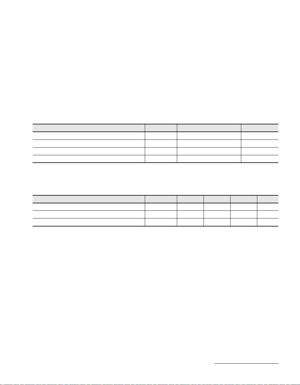
––––––––––––––––––––––––––––––––––––––––––––––––––––––––––––– ■ ML53301/ML53311 TC-622Pro/Pro+ ■
7. TC-622PRO/PRO+ SPECIFICATIONS
This section contains electrical and mechanical specifications common to both the ML53301 TC-622Pro
and ML53311 TC-622Pro+ devices and is divided into the following categories:
• Section 7.1, "Maximum Ratings and Operating Conditions"
• Section 7.2, "DC Characteristics"
• Section 7.3, "AC Specifications"
• Section 7.4, "Mechanical Specifications"
7.1 Maximum Ratings and Operating Conditions
Table 4. Absolute Maximum Ratings
Parameter Symbol Value Unit
Power supply range V
Short circuit output current I
Power dissipation P
Storage temperature T
1. Permanent device damage may occur if the Absolute Maximum Ratings are exceeded. Exposure to absolute maximum rating conditions for extended periods
may affect device reliability.
[1]
CC
OS
STG
-0.5 to +4.0 V
TBD mA
D
TBD W
-55 to+155 °C
Table 5. Recommended Operating Conditions
Parameter Symbol Min. Typ
Recommended Supply Voltage V
Recommended operating temperature T
Supply Current I
1. Voltage with respect to ground unless otherwise specified.
2. Typical figures are at 25°C and are for design aid only; not guaranteed and not subject to production testing.
CC
OP
CC
3.14 3.3 3.46 V
0 — +70 °C
— — 500 mA
[1], [2]
Max. Units
71Oki Semiconductor
Page 78

■ ML53301/ML53311 TC-622Pro/Pro+ ■ –––––––––––––––––––––––––––––––––––––––––––––––––––––––––––––
7.2 DC Characteristics
Table 6. DC Electrical Characteristics (T
Parameter Symbol Conditions Min Typ
Input low voltage
Input high voltage
Output low voltage V
Output low voltage V
Output high voltage V
Output high voltage V
Output rise Time (CMOS) — C
Output rise time (TTL) — — — 2 8 ns
Output fall Time (CMOS) — C
Output fall time (TTL) — — — 2 8 ns
1. Typical figures are at 25°C and are for design aid only; not guaranteed and not subject to production testing.
2. Limited functional test patterns are performed at these input levels. The majority of functional tests are performed at levels of 0 V and 3.3 V.
[2]
[2]
= 0° to 70°C, VCC = 3.3 V ±5%)
A
V
IL
V
IH
OL
OL
OH
OH
— — — 0.8 V
— 2.0 — — V
IOL = 1.6 mA — — 0.4 V
IOL < 10 mA — — 10 %V
IOH = 40 mA 2.4 — — V
IOH < 10 mA 90 — — %V
= 50 pF — 3 8 ns
LOAD
= 50 pF — 3 8 ns
LOAD
[1]
Max Units
CC
CC
7.3 AC Specifications
This section defines the AC timing parameters for the following operations:
• ATM Layer Transmit
• ATM Layer Receive
• Line-Side Transmit
• Line-Side Receive
72 Oki Semiconductor
Page 79
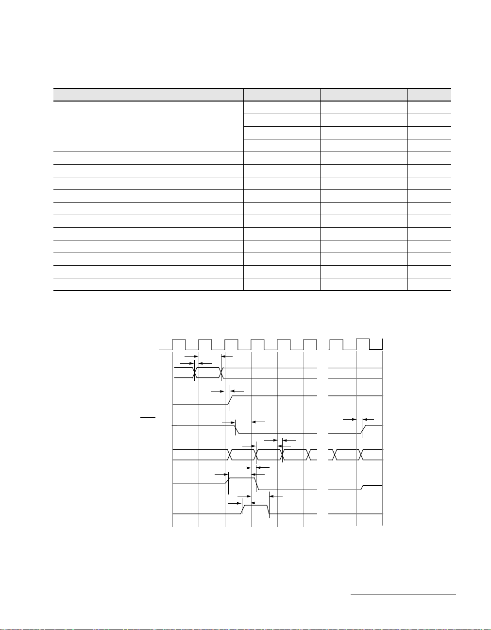
––––––––––––––––––––––––––––––––––––––––––––––––––––––––––––– ■ ML53301/ML53311 TC-622Pro/Pro+ ■
7.3.1 ATM Layer Transmit Table 7. ATM Layer Transmit Timing
Parameter Symbol Min Max Units (ns)
TxCLK General Information frequency -- 50 MHz
duty cycle 40 60 %
peak-to-peak jitter -- .5 %
rise/fall time -- 2 nS
Transmit address setup to TxCLK high t
Transmit address hold from TxCLK high t
TxCLAV output delay from TxCLK high t
Transmit enable setup to TxCLK high t
Transmit enable hold from TxCLK high t
Transmit data setup to TxCLK high t
Transmit data hold from TxCLK high t
Transmit start of cell setup to TxCLK high t
Transmit start of cell hold from TxCLK high t
Transmit parity setup to TxCLK high t
Transmit parity hold from TxCLK high t
STADR
HTADR
HTCLV
STEN
HTEN
STXD
HTXD
STSC
HTXD
STPAR
HTPAR
1.5 nS
3.0 nS
9.0 nS
1.0 nS
3.0 nS
1.0 nS
1.5 nS
1.0 nS
1.0 nS
1.0 nS
1.0 nS
TxCLK
TxADDR[4:0]
TxCLAV
TxENB
TxDATA[15:0]
TxSOC
TxPRTY
t
t
STEN
t
STPAR
t
HTADR
STXD
t
HTCLV
H1 H2 H3
t
HTSC
t
HTPAR
X
t
STADR
X
3-state
t
Addr
STSC
Figure 24. ATM Layer Transmit Timing
t
HTXD
P48
t
3-state
HTEN
73Oki Semiconductor
Page 80

■ ML53301/ML53311 TC-622Pro/Pro+ ■ –––––––––––––––––––––––––––––––––––––––––––––––––––––––––––––
7.3.2 ATM Layer Receive Table 8. ATM Layer Receive Timing
Parameter Symbol Min Max Units (ns)
RxCLK General Information frequency -- 50 MHz
duty cycle 40 60 %
peak-to-peak jitter -- .5 %
rise/fall time -- 2 nS
Receive address setup to RxCLK high t
Receive address hold from RxCLK high t
Receive Clav hold from RxCLK high t
Receive enable setup to RxCLK high t
Receive enable hold from RxCLK high t
Receive data hold from RxCLK high t
Receive start of cell hold from RxCLK high t
Receive parity hold from RxCLK high t
SRADR
HRADR
HRCLV
SREN
HREN
SRXD
HRSC
HRPAR
0.5 nS
2.0 nS
8.0 nS
1.0 nS
3.0 nS
5.0 nS
6.0 nS
7.0 nS
RxCLK
RxADDR[4:0]
RxCLAV
RxENB
RxDATA[15:0]
RxSOC
RxPRTY
t
t
SRADR
X
3-state
t
HRCLV
Addr
HRADR
t
SREN
t
SRXD
H1 H2 H3
t
HRSC
t
HRPAR
Figure 25. ATM Layer Receive Timing
t
HRXD
X
t
HREN
P48
74 Oki Semiconductor
Page 81

––––––––––––––––––––––––––––––––––––––––––––––––––––––––––––– ■ ML53301/ML53311 TC-622Pro/Pro+ ■
7.3.3 Line-Side Transmit Table 9. Line-Side Transmit Timing
Parameter Symbol Min Max Units (ns)
TxBYTECLK General Information frequency -- 77.76 MHz
frequency tolerance -100 +100 ppm
duty cycle 40 60 %
Transmit line data hold from TxBYTECLK high t
Transmit frame hold from TxBYTECLK high t
HTLD
HTFRM
3.6 4.0 nS
14 nS
TxBYTECLK
TxLINEDATA[15:0] Valid
TxFRAME
1 2 3 4 5 6 7
t
HTLD
t
HTFRM
Figure 26. Line-Side Transmit Timing
7.3.4 Line-Side Receive Table 10. Line-Side Receive Timing
Parameter Symbol Min Max Units (ns)
RxBYTECLK General Information frequency -- 77.76 MHz
frequency tolerance -100 +100 ppm
duty cycle 40 60 %
Receive line data setup to RxBYTECLK high t
Receive line data hold from RxBYTECLK high t
Receive frame hold from RxBYTECLK high t
RxBYTECLK
RxLINEDATA[15:0]
RxFRAME
1 2 3 4 5 6 7
t
SRLD
HRFRM
t
HTFRM
SRLD
HRLD
t
HRLD
1.5 nS
4.0 nS
14 nS
Figure 27. Line-Side Receive Timing
75Oki Semiconductor
Page 82

■ ML53301/ML53311 TC-622Pro/Pro+ ■ –––––––––––––––––––––––––––––––––––––––––––––––––––––––––––––
7.4 Mechanical Specifications
Figure 28 shows a package drawing of the 176 pin Plastic LQFP package used in both the ML53301 TC622Pro and ML53311 TC-622Pro+ devices.
26.0 ± 0.2
1.7 max
133
24.0 ± 0.1
176
1.25 typ
1.4 ± 0.05
132
1
0.5 0.22 ± 0.05
89
88
45
44
0.17 ± 0.05
*All measurements are in millimeters.
76 Oki Semiconductor
Figure 28. TC-622Pro/Pro+ Package Drawing
Page 83

––––––––––––––––––––––––––––––––––––––––––––––––––––––––––––– ■ ML53301/ML53311 TC-622Pro/Pro+ ■
8. ML53301 TC-622PRO PCI BUS INTERFACE AND SPECIFICATIONS
This section contains material specific to the ML53301 TC-622Pro and includes the following subsections:
• Section 8.1, "PCI Bus Architectural Overview"
• Section 8.2, "PCI Bus Transactions"
• Section 8.3, "TC-622Pro Signal Descriptions"
• Section 8.4, "PCI Bus AC Specifications"
For MPI bus interface and specification information specific to the ML53311 TC-622Pro+ device, refer to
Section 9.
8.1 PCI Bus Architectural Overview
The TC-622Pro provides a PCI interface for accessing the register array. Registers are mapped to PCI
memory space and can reside within an 8-kbyte space anywhere in memory. Each register requires 4
bytes of address space. Bits [31:9] contain the base address. Bits [8:2] form the register offset. Bit [31] and
bits [1:0] are always zero. Refer to Section 6 for a listing of registers and corresponding offset address values. Figure 29 shows how the PCI bus is partitioned during a register access.
31 30 9 8 2 1 0
0 Base Address Offset Address 00
Figure 29. PCI Address Partitioning During Register Accesses
Figure 30 shows a block diagram of the PCI module. Refer to the main block diagram in Figure 2 for the
relative location of the PCI module in the TC-622Pro.
PCI_INTA
Internal
Signals
PCIIntrReq
RegReady
RegData
RegAddr
RegWrite
RegRead
Interrupt
Control
Register
Control
Data parity error
Address parity error
Target Data
Target Address
Target Control
Swap
Data Out
Parity
Control
Swap
Target
Control
Figure 30. TC-622Pro PCI Architecture Block Diagram
The PCI architecture in Figure 30 contains the following blocks:
• Target Control
• Register Read/Write Control
• Interrupt Control
Swap
Data In
PCI_PAR
PCI_AD[31:0]
PCI_C/BE[3:0]
PCI BUS
PCI_FRAME
PCI_IRDY
PCI_DEVSEL
PCI_LOCK
PCI_TRDY
PCI_STOP
77Oki Semiconductor
Page 84

■ ML53301/ML53311 TC-622Pro/Pro+ ■ –––––––––––––––––––––––––––––––––––––––––––––––––––––––––––––
• Parity Control
• Byte Swap Control
8.1.1 Target Control
The Target block in Figure 30 interfaces with the PCI bus and generates the register control signals. To
access a register, the host drives the PCI_FRAME signal along with PCI_AD[31:0] and PCI_C/BE[3:0].
The target block decodes the address and command signals to determine the location of the register and
the type of operation. This information is passed to the Register Control block. The Target then waits for
the Register Control block to assert its ready signal. The Target then asserts PCI_
TRDY to inform the host
that it is ready for the requested information.
8.1.2 Register Read/Write Control
The Register Control block provides the interface between the Target Control block and the TC-622Pro
registers. The Register Control block accepts the decoded PCI address and command signals from the Tar-
get Control block, then waits for the assertion of an internal RegReady signal. The assertion of this signal
indicates that the requested internal register has been enabled and that the transaction can occur.
8.1.3 Interrupt Control
The Interrupt Control block receives the interrupts from the TC-622Pro and the Parity Control block. Bits of
a register inside the Interrupt Control block are set as interrupts are generated from the various modules
in the TC-622Pro. When a bit is set the Interrupt Control block issues a general interrupt by asserting the
PCI_INTA
signal on the PCI bus. The host responds by reading the interrupt register and then resets the
appropriate bits.
8.1.4 Parity Control
The Parity Control block calculates even parity over the address, data, command, and byte enable busses
for transactions on the PCI bus. Parity generation is required by all PCI agents. In the case of an address
or data parity error, an address or data parity interrupt is generated and passed to the Interrupt Control
block.
The PCI master drives the PCI_PAR signal for address and data write cycles and the Target drives the
PAR signal during read cycles. When address is driven the PCI_PAR signal is valid one clock after
address is driven. When data is driven the PCI_PAR signal is valid one clock after either PCI_
asserted on write transactions, or PCI_
TRDY is asserted on read transactions.
IRDY is
8.1.5 Byte Swap Control
The Byte Swap Control block receives an address from the PCI bus and swaps the address bytes depend-
ing on the requirements of the target.
8.1.6 Register Types
Each internal register is 16-bits wide and is connected to the Register Control block data bus. Seven bits
of address are used to select a particular register. An address decoder generates the register enable signals. There are five register types in the TC-622Pro:
• Read-only
• Read/Write
78 Oki Semiconductor
Page 85

––––––––––––––––––––––––––––––––––––––––––––––––––––––––––––– ■ ML53301/ML53311 TC-622Pro/Pro+ ■
• Read/Write/Set
• Interrupt
• Interrupt Mask
Table 11 shows how the registers are accessed in the TC-622Pro.
Table 11. Accessing the TC-622Pro Registers
Register Type TC-622Pro Access Host Access
Read-only Write-only Read-only
Read/Write Read-only Read/Write
Read/Write/Set Write-only Read/Write
Interrupt Read/Write ---
Interrupt Mask Read/Write ---
Read-only Registers
These registers contain status information for the TC-622Pro. The host can only read these registers and
the TC-622Pro can only write them. When a register has been selected by the address decoder and the
internal RegRead signal is active, the register drives data onto the bus.
Read/Write Registers
These registers contain configuration information for the TC-622Pro. The host can read or write these
registers. The TC-622Pro can only read them. The falling edge of an internal RegWrite signal is used to
latch data into the register selected by the address decoder. When a register is selected and the internal
RegRead signal is active, the register drives data onto the bus.
Read/Write/Set Registers
These registers monitor the performance of the TC-622Pro and contain counters, timers, and accumulator
functions. Register bits are set by signals from the various TC-622Pro modules and are read by the host.
After reading the bits, the host must reset them by writing to that register.
Interrupt Register
The interrupt register contains interrupt status information for the TC-622Pro. The OCD, Loss of Cell
Delineation (LCD), Loss of Frame (LOF), and Out of Frame (OOF) lines are used to generate the interrupt. The register bits are set when these signals are asserted by the corresponding state machines. The
interrupt register bits are used to assert the PCI_INTA
signal on the PCI bus. Whenever the interrupt is
generated the corresponding bit in the register is reset by the Interrupt Control block.
Interrupt Mask Register
The interrupt mask register contains the interrupt mask status bits of the TC-622Pro. If an interrupt mask
bit is set, the corresponding interrupt is masked from generating an interrupt. This register is controlled
by the Interrupt Control block.
79Oki Semiconductor
Page 86

■ ML53301/ML53311 TC-622Pro/Pro+ ■ –––––––––––––––––––––––––––––––––––––––––––––––––––––––––––––
8.2 PCI Bus Transactions
Figure 31 and Figure 32 show the basic read and write transactions on the PCI bus.
PCI Bus Signals
PCI Bus Signals
PCI_CLK
PCI_AD[31:0]
PCI_FRAME
PCI_IRDY
PCI_DEVSEL
PCI_TRDY
PCICLK
PCI_AD[31:0]
PCI_FRAME
PCI_IRDY
PCI_DEVSEL
PCI_TRDY
1 2 3 4 5 6 7 8 9 10
Data 1 Data 2Addr
Figure 31. PCI Read Transaction
1 2 3 4 5 6 7 8 9 10
Addr
Data 1
Data 2
80 Oki Semiconductor
Figure 32. PCI Write Transaction
Page 87

––––––––––––––––––––––––––––––––––––––––––––––––––––––––––––– ■ ML53301/ML53311 TC-622Pro/Pro+ ■
8.3 TC-622Pro Signal Descriptions
This section provides the pin descriptions for the ML53301 TC-622Pro device. The pin descriptions are
divided into four tables for the transmit interface, receive interface, PCI interface, and general signals.
Alphabetical and numerical pin listings are also provided.
Figure 33 shows a diagram of the TC-622Pro signal groupings.
Transmit Interface
Receive Interface
TxLINEDATA[7:0]
TxCLK
TxENB
TxADDR[4:0]
TxDATA[15:0]
TxSOC
TxPRTY
TxCLAV
TxFRAME
RxBYTECLK
RxLINEDATA[7:0]
RxLINELOC
RxLINELOS
RxLOF
RxLCD[3:0]
RxCLK
RxENB
RxADDR[4:0]
RxDATA[15:0]
RxSOC
RxPRTY
RxCLAV
RxFRAME
PCI_CLKTxBYTECLK
PCI_RST
PCI_AD[31:0]
PCI_C/BE[3:0]
PCI_PAR
PCI_FRAME
PCI_IRDY
PCI_TRDY
PCI_STOP
PCI_LOCK
PCI_IDSEL
PCI_DEVSEL
PCI_SERR
PCI_PERR
PCI_INTA
TEST_HOLD
TEST_SE
TEST_SI[12:1]
TEST_SO[12:1]
RESET
Figure 33. ML53301 TC-622PRO Logic Symbol
PCI Interface
Test Interface
Configuration
Interface
81Oki Semiconductor
Page 88

■ ML53301/ML53311 TC-622Pro/Pro+ ■ –––––––––––––––––––––––––––––––––––––––––––––––––––––––––––––
Table 12. TC-622PRO Transmit Interface Signals
Pin Name Pin Type Description
Transmit UTOPIA Interface
TxADDR[4:0] I 5-bit transmit UTOPIA port address. These pins are used to address up to a maximum of 32
TxCLAV O This signal is driven by the UTOPIA to the ATM layer device and indicates that one or more buffer
TxCLK I 50 MHz clock for the transmit UTOPIA. This clock is used to transfer data between the UTOPIA and
TxDATA[15:0] I 16-bit transmit UTOPIA data bus. This unidirectional bus is driven by the ATM layer device to the
TxENB
TxPRTY I Parity for the incoming data from the ATM layer device.
TxSOC I During a transmit operation, this signal is asserted for one clock by the ATM layer device at the start
Transmit Line Interface
TxBYTECLK I Transmit byte clock. This signal is used to transfer data between the transmit framer and the
TxFRAME O A one transmit byte pulse for every frame transmitted to the external parallel-to-serial converter.
TxLINEDATA[7:0] O This 8-bit data value is driven by the transmit framer and connects to an external parallel-to-serial
I Transmit UTOPIA enable. TxENB is asserted by the ATM layer device whenever valid data is on
transmit ports. The TC-622Pro contains 4 transmit ports.
spaces are available.
the ATM layer device.
TC-622Pro during a transmit operation.
the bus. When TxENB
of a cell transmission.
external parallel-to-serial converter. The clock operates at 77.76 MHz (622.08/8)
converter.
is deasserted the data bus is tri-stated.
82 Oki Semiconductor
Page 89

––––––––––––––––––––––––––––––––––––––––––––––––––––––––––––– ■ ML53301/ML53311 TC-622Pro/Pro+ ■
Table 13. TC-622PRO Receive Interface Signals
Pin Name Pin Type Description
Receive UTOPIA Interface
RxADDR[4:0] I 5-bit transmit receive UTOPIA port address. These pins are used to address up to a maximum of
RxCLAV O This signal is driven by the receive UTOPIA to the ATM layer device and indicates that one or more
RxCLK I 50 MHz clock for the receive UTOPIA. This clock is used to transfer data between the receive
RxDATA[15:0] O 16-bit receive UTOPIA data bus. This unidirectional bus is used by the TC-622Pro to drive data to
RxENB
RxPRTY O This signal is driven by the TC-622Pro and is the parity for the outgoing data to the ATM layer
RxSOC O During a receive operation this signal is asserted by the TC-622Pro for one clock to indicate the
Receive Line Interface
RxBYTECLK I Receive byte clock. This signal is used to transfer data between the external parallel-to-serial
RxFRAME O A one receive byte pulse for every frame received from the serial-to-parallel converter.
RxLCD[3:0] O Indicates a loss of cell delineation. This signal is asserted when cell delineation has not been
RxLINEDATA[7:0] I This 8-bit data value is driven by the external parallel-to-serial converter and connects to the receive
RxLINELOC I Assertion of this signal indicates a loss of clock from the external recovery module.
RxLINELOS I Assertion of this signal indicates a loss of signal from the external recovery module.
RxLOF O Indicates a loss of framing. This alarm signal is asserted when the receive framer is not able to
I Receive UTOPIA enable. RxENB is asserted by the ATM layer device whenever valid data is on
32 receive ports. The TC-622Pro contains 4 receive ports.
buffer spaces are available.
UTOPIA and the ATM layer device.
the ATM layer device during a receive operation.
the bus. When RxENB
device.
start of a cell transmission.
converter and the receive framer. The clock operates at 77.76 MHz (622.08/8)
achieved for more than 4 mS. In the presence of an LOS, LOF, or LOC alarm this signal is not
asserted.
framer.
transition to the SYNC state for more than 3 mS. The signal is deasserted 1 mS after the receive
framer enters the SYNC state.
is deasserted the data bus is tri-stated.
83Oki Semiconductor
Page 90
■ ML53301/ML53311 TC-622Pro/Pro+ ■ –––––––––––––––––––––––––––––––––––––––––––––––––––––––––––––
Table 14. TC-622Pro PCI Interface Signals
Pin Name Pin Type Description
PCI_AD[31:0] I/O Multiplexed PCI address and data bus. During a bus operation, address is driven for one clock,
PCI_C/BE[3]
PCI_C/BE[2]
PCI_C/BE[1]
PCI_C/BE[0]
PCI_DEVSEL/TEST_SO12 I/O Device select. When an address is driven by the host, this signal is driven by the TC-622Pro to
PCI_IDSEL/TEST_SI12 I Initialization device select. This signal functions as an initialization select signal for the PCI device
PCI_INTA
PCI_IRDY
PCI_LOCK
PCI_PAR/TEST_SO11 I/O This signal is driven by the host during a write operation and by the TC-622Pro during a read
PCI_PERR
PCI_SERR
PCI_STOP
PCI_TRDY
/TEST_SI6
/TEST_SI7
/TEST_SI8
/TEST_SI9
PCI_CLK I 33 MHz PCI clock. All PCI bus signals except PCI_RST
PCI_FRAME
/TEST_SO10 O TC-622Pro interrupt. This signal is asserted by the TC-622Pro to request an interrupt from the host.
/TEST_SI11 I Initiator ready signal. This signal is asserted by the current master to indicate its ability to complete
/TEST_SI10 I This signal is asserted by the host to indicate an atomic transfer operation between the host and
/TEST_SO7 O Parity error indication. This signal is asserted by the TC-622Pro to indicate a data parity error during
PCI_RST
/TEST_SO8 O System error indication. PCI_SERR is asserted by the TC-622Pro to indicate that an address parity
/TEST_SO6 O Transaction Stop Request. PCI_STOP is asserted by the TC-622Pro to request the host to stop the
/TEST_SO9 O Target ready indication. PCI_TRDY is asserted by the TC-622Pro to indicate its ability to complete
I This 4-bit bus multiplexes the PCI bus commands and byte enables. Command information is
I The cycle frame is driven by the host to indicate the beginning and duration of an operation. This
I PCI Reset. PCI_RST is driven by the host and is used to initialize PCI-specific registers,
followed by data. On a read operation data is driven by the TC-622Pro. On a write operation data
is driven by the host. This bus can be tri-stated.
driven by the host at the same time as address is driven on PCI_AD[31:0]. Byte enable information
is driven along with data.
The PCI_C/BE[3]
The PCI_C/BE[2]
The PCI_C/BE[1]
The PCI_C/BE[0]
The test scan signals are used during manufacturing test and do not effect the normal operation of
the byte enables.
the rising edge of this clock.
indicate that the address has been decoded. As an input, this signal indicates whether the device
has been selected. This signal is shared with test scan output 12.
signal is asserted while data is being transferred and deasserted when the data transfer has been
completed.
configuration registers. PCI_IDSEL is an input to the TC-622Pro and can be used as a chip select
during a PCI register access. This signal is shared with test scan input 12.
PCI_INTA
test scan output 10.
the current data phase of a transaction. This signal is shared with test scan input 11.
the TC-622Pro is in progress. This signal is shared with test scan input 10.
operation. PCI_PAR represents even parity across the PCI_AD[31:0] and PCI_C/BE[3:0]
This signal has the same timing as PCI_AD[31:0] but is delayed by one clock. PCI_PAR can be tristated. This signal is shared with test scan output 11.
the data transfer. Parity error are reported on all PCI transactions except special cycles. This signal
is shared with test scan output 7.
sequencers, and signals.
error has been detected. This signal is shared with test scan output 8.
current transaction. This signal is shared with test scan output 6.
the current data phase of a transaction. This signal is shared with test scan output 9.
signal is shared with test scan input 6.
signal is shared with test scan input 7.
signal is shared with test scan input 8.
signal is shared with test scan input 9.
and PCI_INTA are driven or sampled on
is level-sensitive and is tri-stated when PCI_RST is asserted. This signal is shared with
signals.
84 Oki Semiconductor
Page 91

––––––––––––––––––––––––––––––––––––––––––––––––––––––––––––– ■ ML53301/ML53311 TC-622Pro/Pro+ ■
Table 15. TC-622PRO Configuration Interface Signals
Pin Name Pin Type Description
RESET
I Asynchronous reset signal for the TC-622Pro. Assertion of this signal resets all internal flip-flops.
Table 16. TC-622PRO Test interface Signals
Pin Name Pin Type Description
TEST_HOLD I Used for test scan purposes during manufacturing. This pin should be tied to ground.
TEST_SE I Used for test scan purposes during manufacturing. This pin should be tied to ground.
TEST_SI[12:1] I Used for test scan purposes during manufacturing. These pins should be tied to ground.
TEST_SO[12:1] O Used for test scan purposes during manufacturing. These pins should be left unconnected.
85Oki Semiconductor
Page 92

■ ML53301/ML53311 TC-622Pro/Pro+ ■ –––––––––––––––––––––––––––––––––––––––––––––––––––––––––––––
Table 17. TC-622PRO Alphabetical Pin List
Pin Name Pin Pin Name Pin Pin Name Pin Pin Name Pin Pin Name Pin
PCI_CLK 31 PCI_C/BE[2]
NC 37 PCI_C/BE[3
PCI_AD[0] 46 PCI_DEVSEL
PCI_AD[1] 47 PCI_FRAME
PCI_AD[2] 49 PCI_IDSEL/TEST_SI12 33 RxFRAME 3 TxCLAV 83 VDD 99
PCI_AD[3] 50 PCI_INTA
PCI_AD[4] 52 PCI_IRDY
PCI_AD[5] 53 PCI_LOCK
PCI_AD[6] 55 PCI_PAR/TEST_SO11 38 RxLCD[3] 9 TxDATA[2] 136 VDDC 73
PCI_AD[7] 56 PCI_PERR
PCI_AD[8] 58 PCI_SERR
PCI_AD[9] 59 PCI_STOP
PCI_AD[10] 61 PCI_TRDY
PCI_AD[11] 62 RESET
PCI_AD[12] 64 PCI_RST
PCI_AD[13] 65 RxADDR[0] 21 RxLINEDATA[6] 17 TxDATA[9] 143 VSS 48
PCI_AD[14] 66 RxADDR[1] 22 RxLINEDATA[7] 18 TxDATA[10] 144 VSS 54
PCI_AD[15] 68 RxADDR[2] 23 RxLINELOC 19 TxDATA[11] 145 VSS 57
PCI_AD[16] 70 RxADDR[3] 24 RxLINELOS 20 TxDATA[12] 146 VSS 63
PCI_AD[17] 89 RxADDR[4] 25 RxLOF 5 TxDATA[13] 147 VSS 67
PCI_AD[18] 91 RxBYTECLK 153 RxPRTY 27 TxDATA[14] 148 VSS 72
PCI_AD[19] 92 RxCLAV 28 RxSOC 26 TxDATA[15] 149 VSS 77
PCI_AD[20] 94 RxCLK 117 TEST_HOLD 71 Tx_ENB
PCI_AD[21] 95 RxDATA[0] 112 TEST_SE 157 TxFRAME 4 VSS 101
PCI_AD[22] 97 RxDATA[1] 113 TEST_SI1 132 TxLINEDATA[0] 164 VSS 106
PCI_AD[23] 98 RxDATA[2] 114 TEST_SI2 131 TxLINEDATA[1] 165 VSS 116
PCI_AD[24] 100 RxDATA[3] 115 TEST_SI3 156 TxLINEDATA[2] 166 VSS 124
PCI_AD[25] 102 RxDATA[4] 118 TEST_SI4 155 TxLINEDATA[3] 167 VSS 151
PCI_AD[26] 103 RxDATA[5] 119 TEST_SI5 154 TxLINEDATA[4] 168 VSSC 81
PCI_AD[27] 105 RxDATA[6] 120 TEST_SO1 163 TxLINEDATA[5] 169 VSSC 96
PCI_AD[28] 107 RxDATA[7] 121 TEST_SO2 162 TxLINEDATA[6] 170 VSSC 158
PCI_AD[29] 108 RxDATA[8] 122 TEST_SO3 161 TxLINEDATA[7] 171 VSSC 176
PCI_AD[30] 110 RxDATA[9] 123 TEST_SO4 160 TxPRTY 78
PCI_AD[31] 111 RxDATA[10] 125 TEST_SO5 159 TxSOC 79
PCI_C/BE[0]
PCI_C/BE[1]
/TEST_SI9 39 RxDATA[11] 126 TxADDR[0] 88 VDD 34
/TEST_SI8 41 RxDATA[12] 127 TxADDR[1] 87 VDD 43
/TEST_SI7 42 RxDATA[13] 128 TxADDR[2] 86 VDD 51
]/TEST_SI6 44 RxDATA[14] 129 TxADDR[3] 85 VDD 60
/TEST_SO12 76 RxDATA[15] 130 TxADDR[4] 84 VDD 69
36 RxENB 29 TxBYTECLK 150 VDD 90
/TEST_SO10 173 RxLCD[0] 6 TxCLK 82 VDD 104
/TEST_SI11 35 RxLCD[1] 7 TxDATA[0] 134 VDD 152
/TEST_SI10 174 RxLCD[2] 8 TxDATA[1] 135 VDDC 2
/TEST_SO7 74 RxLINEDATA[0] 11 TxDATA[3] 137 VDDC 109
/TEST_SO8 75 RxLINEDATA[1] 12 TxDATA[4] 138 VDDC 133
/TEST_SO6 175 RxLINEDATA[2] 13 TxDATA[5] 139 VDDC 172
/TEST_SO9 40 RxLINEDATA[3] 14 TxDATA[6] 140 VSS 10
1 RxLINEDATA[4] 15 TxDATA[7] 141 VSS 32
30 RxLINEDATA[5] 16 TxDATA[8] 142 VSS 45
80 VSS 93
86 Oki Semiconductor
Page 93

––––––––––––––––––––––––––––––––––––––––––––––––––––––––––––– ■ ML53301/ML53311 TC-622Pro/Pro+ ■
Table 18. TC-622PRO Numerical Pin List
Pin Pin Name Pin Pin Name Pin Pin Name Pin Pin Name Pin Pin Name
1 RESET 37 NC 73 VDDC 109 VDDC 145 TxDATA[11]
2 VDDC 38 PCI_PAR/TEST_SO11 74 PCI_PERR
3 RxFRAME 39 PCI_C/BE[0]
4 TxFRAME 40 PCI_TRDY
5 RxLOF 41 PCI_C/BE[1]
6 RxLCD[0] 42 PCI_C/BE[2]
7 RxLCD[1] 43 VDD 79 TxSOC 115 RxDATA[3] 151 VSS
8 RxLCD[2] 44 PCI_C/BE[3]
9 RxLCD[3] 45 VSS 81 VSSC 117 RxCLK 153 RxBYTECLK
10 VSS 46 PCI_AD[0] 82 TxCLK 118 RxDATA[4] 154 TEST_SI5
11 RxLINEDATA[0] 47 PCI_AD[1] 83 TxCLAV 119 RxDATA[5] 155 TEST_SI4
12 RxLINEDATA[1] 48 VSS 84 TxADDR[4] 120 RxDATA[6] 156 TEST_SI3
13 RxLINEDATA[2] 49 PCI_AD[2] 85 TxADDR[3] 121 RxDATA[7] 157 TEST_SE
14 RxLINEDATA[3] 50 PCI_AD[3] 86 TxADDR[2] 122 RxDATA[8] 158 VSSC
15 RxLINEDATA[4] 51 VDD 87 TxADDR[1] 123 RxDATA[9] 159 TEST_SO5
16 RxLINEDATA[5] 52 PCI_AD[4] 88 TxADDR[0] 124 VSS 160 TEST_SO4
17 RxLINEDATA[6] 53 PCI_AD[5] 89 PCI_AD[17] 125 RxDATA[10] 161 TEST_SO3
18 RxLINEDATA[7] 54 VSS 90 VDD 126 RxDATA[11] 162 TEST_SO2
19 RxLINELOC 55 PCI_AD[6] 91 PCI_AD[18] 127 RxDATA[12] 163 TEST_SO1
20 RxLINELOS 56 PCI_AD[7] 92 PCI_AD[19] 128 RxDATA[13] 164 TxLINEDATA[0]
21 RxADDR[0] 57 VSS 93 VSS 129 RxDATA[14] 165 TxLINEDATA[1]
22 RxADDR[1] 58 PCI_AD[8] 94 PCI_AD[20] 130 RxDATA[15] 166 TxLINEDATA[2]
23 RxADDR[2] 59 PCI_AD[9] 95 PCI_AD[21] 131 TEST_SI2 167 TxLINEDATA[3]
24 RxADDR[3] 60 VDD 96 VSSC 132 TEST_SI1 168 TxLINEDATA[4]
25 RxADDR[4] 61 PCI_AD[10] 97 PCI_AD[22] 133 VDDC 169 TxLINEDATA[5]
26 RxSOC 62 PCI_AD[11] 98 PCI_AD[23] 134 TxDATA[0] 170 TxLINEDATA[6]
27 RxPRTY 63 VSS 99 VDD 135 TxDATA[1] 171 TxLINEDATA[7]
28 RxCLAV 64 PCI_AD[12] 100 PCI_AD[24] 136 TxDATA[2] 172 VDDC
29 RxENB 65 PCI_AD[13] 101 VSS 137 TxDATA[3] 173 PCI_INTA
30 PCI_RST
31 PCI_CLK 67 VSS 103 PCI_AD[26] 139 TxDATA[5] 175 PCI_STOP
32 VSS 68 PCI_AD[15] 104 VDD 140 TxDATA[6] 176 VSSC
33 PCI_IDSEL/TEST_SI12 69 VDD 105 PCI_AD[27] 141 TxDATA[7]
34 VDD 70 PCI_AD[16] 106 VSS 142 TxDATA[8]
35 PCI_IRDY
36 PCI_FRAME
/TEST_SI11 71 TEST_HOLD 107 PCI_AD[28] 143 TxDATA[9]
66 PCI_AD[14] 102 PCI_AD[25] 138 TxDATA[4] 174 PCI_LOCK/TEST_SI10
72 VSS 108 PCI_AD[29] 144 TxDATA[10]
/TEST_SI9 75 PCI_SERR/TEST_SO8 111 PCI_AD[31] 147 TxDATA[13]
/TEST_SO9 76 PCI_DEVSEL/TEST_SO12 112 RxDATA[0] 148 TxDATA[14]
/TEST_SI8 77 VSS 113 RxDATA[1] 149 TxDATA[15]
/TEST_SI7 78 TxPRTY 114 RxDATA[2] 150 TxBYTECLK
/TEST_SI6 80 Tx_ENB 116 VSS 152 VDD
/TEST_SO7 110 PCI_AD[30] 146 TxDATA[12]
/TEST_SO10
/TEST_SO6
87Oki Semiconductor
Page 94

■ ML53301/ML53311 TC-622Pro/Pro+ ■ –––––––––––––––––––––––––––––––––––––––––––––––––––––––––––––
8.4 PCI Bus AC Specifications
8.4.1 PCI Bus Register Write Table 19. PCI Bus Register Write Timing
Parameter Symbol Min Max Units (ns)
PCI_CLK clock frequency PCI
PCI_IDSEL to PCI clock setup time PCI
PCI clock to PCI_IDSEL hold time PCI
PCI_C/BE[3:0]
PCI clock to PCI_C/BE[3:0]
PCI_AD[31:0] to PCI clock setup time PCI
PCI clock to PCI_AD[31:0] hold time (input) PCI
PCI_FRAME
PCI clock to PCI_FRAME
PCI_IRDY to PCI clock setup time PCI
PCI clock to PCI_IRDY
PCI clock to PCI_DEVSEL
PCI clock to PCI_PERR
PCI clock to PCI_SERR
PCI clock to PCI_TRDY
PCI_PAR (input) to PCI clock setup time PCI
PCI clock to PCI_PAR (input) hold time PCI
PCI clock to PCI_PAR output delay PCI
1. All output delays assume loading of 50 pF.
to PCI clock setup time PCI
hold time PCI
to PCI clock setup time PCI
hold time PCI
hold time PCI
output delay PCI
output delay PCI
output delay PCI
output delay PCI
[1]
CLKFR
IDSU
IDHLD
CBESU
CBEHLD
ADSU
ADHLDI
FRMSU
FRMHLD
IRDYSU
IRDYHLD
CLKDVSL
CLKPERR
CLKSERR
CLKTRDY
PARSU
PARHLD
CLKPAR
0 MHz 33 MHz nS
1.0 1.9 nS
4.1 5.1 nS
0.3 1.5 nS
1.3 3.6 nS
1.5 6.5 nS
3.7 8.8 nS
2.3 8.7 nS
4.5 10.8 nS
2.3 8.7 nS
4.4 11 nS
5.2 15.7 nS
3.98 7.75 nS
nS
5.0 10.9 nS
0.8 3.9 nS
2.6 2.4 nS
4.3 8.2 nS
88 Oki Semiconductor
Page 95
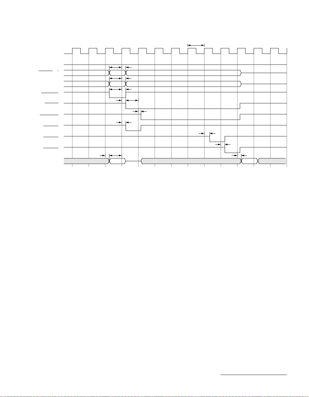
––––––––––––––––––––––––––––––––––––––––––––––––––––––––––––– ■ ML53301/ML53311 TC-622Pro/Pro+ ■
PCI
PCI_CLK
CLFKR
PCI_IDSEL
PCI_C/BE[3:0]
PCI_AD[31:0]
PCI_FRAME
PCI_IRDY
PCI_DEVSEL
PCI_PERR
PCI_SERR
PCI_TRDY
PCI_PAR
PCI
CLKDVSL
PCI
PARHLD
PCI
PCI
PCI
CBEHLD
ADHLD
FRMHLD
PCI
IRDYHLD
Valid Write Data
PCI
CLKSERR
PCI
PARSU
PCI
PCI
CBESU
Valid
PCI
ADSU
Valid
FRMSU
PCI
IRDYSU
PCI
CLKPERR
Valid Valid
Figure 34. PCI Bus Register Write Timing Diagram
PCI
CLKTRDY
PCI
CLKPAR
89Oki Semiconductor
Page 96

■ ML53301/ML53311 TC-622Pro/Pro+ ■ –––––––––––––––––––––––––––––––––––––––––––––––––––––––––––––
8.4.2 PCI Bus Register Read Table 20. PCI Bus Register Read Timing
Parameter Symbol Min Max Units
PCI_CLK clock frequency PCI
PCI_IDSEL to PCI clock setup time PCI
PCI clock to PCI_IDSEL hold time PCI
PCI_C/BE[3:0]
PCI clock to PCI_C/BE[3:0]
PCI_AD[31:0] to PCI clock setup time PCI
PCI clock to PCI_AD[31:0] hold time PCI
PCI clock to read data valid delay PCI
PCI_FRAME
PCI clock to PCI_FRAME
PCI_IRDY to PCI clock setup time PCI
PCI clock to PCI_IRDY
PCI clock to PCI_DEVSEL
PCI clock to PCI_TRDY
PCI_PAR to PCI clock input setup time PCI
PCI clock to PCI_PAR input hold time PCI
PCI clock to PCI_PAR output delay PCI
PCI clock to PCI_STOP
PCI clock to PCI_INTA
1. All output delays assume loading of 50 pF.
to PCI clock setup time PCI
hold time PCI
to PCI clock setup time PCI
hold time PCI
hold time PCI
output delay PCI
output delay PCI
output delay PCI
output delay PCI
[1]
CLKFR
IDSU
IDHLD
CBESU
CBEHLD
ADSU
ADHLD
DTOUT
FRMSU
FRMHLD
IRDYSU
IRDYHLD
CLKDVSL
CLKTRDY
PARSU
PARHLD
CLKPAR
STOP
INTA
0 MHz 33 MHz nS
1.0 1.9 nS
4.1 5.1 nS
0.3 1.5 nS
1.3 3.6 nS
1.5 6.5 nS
1.3 3.6 nS
4 PCI_CLK + 4 ns 8 PCI_CLK + 13 ns nS
2.3 8.7 nS
4.5 10.8 nS
2.3 8.7 nS
4.4 11.0 nS
5.2 15.7 nS
5.0 10.9 nS
0.8 3.9 nS
2.6 2.4 nS
4.3 8.2 nS
5.4 10.9 nS
23.8 27.5 nS
90 Oki Semiconductor
Page 97

––––––––––––––––––––––––––––––––––––––––––––––––––––––––––––– ■ ML53301/ML53311 TC-622Pro/Pro+ ■
PCI_CLK
PCI_IDSEL
PCI_C/BE[3:0] Valid
PCI_AD[31:0] Valid
PCI_FRAME
PCI_IRDY
PCI_DEVSEL
PCI_PERR
PCI_SERR
PCI_TRDY
PCI_PAR Valid
PCI
PCI
PCI
PCI
PARSU
CBESU
ADSU
FRMSU
PCI
PCI
CLKPERR
IRDYSU
PCI
PCI
PCI
PCI
PCI
CLKDVSL
PARHLD
CBEHLD
ADHLD
FRMHLD
PCI
IRDYHLD
Invalid
PCI
CLKSERR
PCI
CLKTRDY
PCI
Valid
CLKPAR
Valid
Figure 35. PCI Bus Register Read Timing Diagram
8.4.3 PCI Bus Configuration Write
The timing parameters in Figure 36 are the same as for the PCI Bus Register Write. Refer to Table 19 for
timing information.
PCI_CLK
PCI_IDSEL
PCI_C/BE[3:0]
PCI_AD[31:0]
PCI_FRAME
PCI_IRDY
PCI_DEVSEL
PCI_TRDY
PCI_STOP
Figure 36. PCI Configuration Write Timing Diagram
91Oki Semiconductor
Page 98

■ ML53301/ML53311 TC-622Pro/Pro+ ■ –––––––––––––––––––––––––––––––––––––––––––––––––––––––––––––
8.4.4 PCI Bus Configuration Read
The timing parameters in Figure 37 are the same as for the PCI Bus Register Read. Refer to Table 20 for
timing information.
PCI_CLK
PCI_IDSEL
PCI_C/BE[3:0]
PCI_AD[31:0]
PCI_FRAME
PCI_IRDY
PCI_DEVSEL
PCI_TRDY
PCI_STOP
Figure 37. PCI Configuration Read Timing Diagram
92 Oki Semiconductor
Page 99

––––––––––––––––––––––––––––––––––––––––––––––––––––––––––––– ■ ML53301/ML53311 TC-622Pro/Pro+ ■
9. ML53311 TC-622PRO+ MPI BUS INTERFACE AND SPECIFICATIONS
This section contains material specific to the ML53311 TC-622Pro+ and includes the following subsections:
• Section 9.1, "MPI Bus Architectural Overview"
• Section 9.2, "MPI Bus Transactions"
• Section 9.3, "TC-622Pro+ Signal Descriptions"
• Section 9.4, "MPI Bus AC Specifications"
For PCI bus interface and specification information specific to the ML53301 TC-622Pro device, refer to
Section 8.
9.1 MPI Bus Architectural Overview
The TC-622Pro+ provides a microprocessor interface (MPI) bus for accessing the register array. The MPI
bus is intended for use in low-cost applications where a full PCI interface is not required. In the TC622Pro+ registers are accessed directly by driving the required address onto the bus. No memory mapping of registers is required. This differs from the TC-622Pro where all registers are memory-mapped to
a specific 8-kbyte space and accessed through the PCI bus. In MPI mode the registers are not memory
mapped and are accessed directly using a separate 7-bit address bus.
In the TC-622Pro+ an MPI bus memory access is initiated by driving the address onto MPI_ADDR[6:0].
The host drives data to the TC-622Pro+ on a write operation. The TC-622Pro+ drives data to the host during a read operation. The host asserts the MPI_R/W
these signals are in their proper state, the host asserts MPI_CS
All 16-bit MPI interface signals are asynchronous to the CPU clock.
Figure 38 shows the TC-622Pro+ bus format during a register access. Note that the address bus is physically separate from the data bus, rather than multiplexed as in the TC-622Pro. Each address on
MPI_ADDR[6:0] corresponds to a 16-bit value. All TC-622Pro+ registers are 16-bits wide except for the
32-bit Interrupt and Interrupt Mask registers whose upper 16 bits are unused.
signal to indicate a read or write operation. Once
to initiate the TC-622Pro+ register access.
15 0
MPI_DATA[15:0]
MPI_ADDR[6:0]
7
0
Register Address
Register Data
Figure 38. Addressing the TC-622Pro+ Registers Via the 16-bit MPI Interface
9.2 MPI Bus Transactions
This section discusses the MPI bus transaction timings during a register read and a register write.
9.2.1 MPI Bus Register Read
When the host requests a 16-bit read, the TC-622Pro+ fetches all 16 bits of register data, latches the data
into the MPI Data Path block, and drives it onto the bus. The MPI_RDY
622Pro+ to indicate when valid register data is available on MPI_DATA[15:0]. The TC-622Pro+ deasserts
MPI_RDY
622Pro+ asserts MPI_RDY
by default at the start of the transaction to indicate that data is not yet available. The TC-
whenever valid data is driven onto the bus.
signal is driven by the TC-
93Oki Semiconductor
Page 100

■ ML53301/ML53311 TC-622Pro/Pro+ ■ –––––––––––––––––––––––––––––––––––––––––––––––––––––––––––––
Although externally the MPI_CS signal is asserted asynchronous to the CPU clock, it is synchronized
with the CPU clock internally. The setup and hold times for MPI_DATA[15:0] and MPI_R/W
to the falling edge of MPI_CS
.
are relative
Figure 39 shows a timing diagram of a 16-bit register read operation. A numbered sequence following the
diagram describes the transaction flow on a clock-by-clock basis. The numbers reference each clock in the
diagram.
MPI_CLK
MPI_ADDR[6:0]
MPI_DATA[15:0]
MPI_R/W
MPI_CS
MPI_RDY
1234567
Valid
xxxxxxx
Sampled active by the TC-622Pro+
Valid
Invalid
Figure 39. TC-622Pro+ 16-Bit Register Read
1. In clock 1 the host drives address onto MPI_ADDR[6:0] and the MPI_R/W
read operation. The host then asserts the MPI_CS
2. In clock 2 the host continues to drive MPI_CS
signal to enable the TC-622Pro+ register array.
. The TC-622Pro+ samples MPI_CS active at the rising
signal high to indicate a
edge of clock 2 and latches the address and control information into the MPI data path block. Note
that a minimum of two clocks is required between the time that MPI_CS
622Pro+ and the time that data is valid on the bus. The host can continue to drive the MPI_R/W
is sampled active by the TC-
signal throughout the read transaction, although they are only required to be driven for one clock. Once
a cycle has completed, the TC-622Pro+ always reverts the data bus to input mode (default for write
cycles). Therefore, when the TC-622Pro+ samples MPI_CS
asserted at the rising edge of clock 2, the
remainder of clock 2 is used for bus turnaround.
3. In clock 3 the host continues to drive the MPI_CS, MPI_ADDR[6:0], and MPI_R/W signals. The TC622Pro+ drives valid data onto the bus in clock 3.
4. In clock 4 the TC-622Pro+ asserts the MPI_RDY signal to indicate that valid data is on the bus. The
host continues to drive the MPI_ADDR[6:0], MPI_CS
and MPI_R/W signals until MPI_RDY is sam-
pled asserted at the rising edge of clock 5.
5. Once the host has sampled MPI_RDY asserted, the host latches data and stops driving the
MPI_ADDR[6:0] and MPI_R/W
response to the deassertion of MPI_CS
MPI_RDY
.
signals and deasserts MPI_CS, indicating the end of the cycle. In
by the host, the TC-622Pro+ asynchronously deasserts
9.2.2 MPI Bus Register Write
When the host requests a 16-bit write, the TC-622Pro+ latches the address, control, and incoming data
into the MPI Data Path block. By default the TC-622Pro+ deasserts MPI_RDY
tion to indicate that data is not yet available. The TC-622Pro+ asserts MPI_RDY
at the start of any transac-
during a write operation
to indicate that it has accepted the data on MPI_DATA[15:0].
94 Oki Semiconductor
 Loading...