

ML2612 FAMILY DATASHEET
ML2612 FAMILY DATASHEET
(DIGEST)
Version 3
Revised on 31-Oct-07
Version: 3
1

ML2612 FAMILY DATASHEET
Contents
Contents...................................................................................................................................................................................................2
General Description.................................................................................................................................................................................3
Features ...................................................................................................................................................................................................3
Block Diagram ........................................................................................................................................................................................5
Application Example ...............................................................................................................................................................................6
Pin Layout ...............................................................................................................................................................................................8
Pin Description......................................................................................................................................................................................10
Absolute Maximum Ratings..................................................................................................................................................................12
Recommended Operating Condition .....................................................................................................................................................12
Electrical Characteristics.......................................................................................................................................................................13
DC Characteristics ............................................................................................................................................................................13
Power Consumption..........................................................................................................................................................................14
AC Characteristics ............................................................................................................................................................................15
Clock......................................................................................................................................................................... 15
Reset .........................................................................................................................................................................15
2 wire serial interface................................................................................................................................................ 16
3 wire serial interface................................................................................................................................................ 17
SAI (Slave) ............................................................................................................................................................... 18
SAI (Master)............................................................................................................................................................. 19
Digital Microphone Interface.................................................................................................................................... 20
Power Supply Sequence....................................................................................................................................................................21
Analog Characteristics ......................................................................................................................................................................23
Digital Filter Characteristics .............................................................................................................................................................25
Revision history....................................................................................................................................................................................26
Version: 3
2

ML2612 FAMILY DATASHEET
General Description
The ML2612 family is a low power small size monaural CODEC with in-built speaker amplifier, ideally suited for
portable playback and recording applications. The microphone interface (1bit digital) supports MEMS (silicon) digital
microphones for low noise recording systems. For digital signal processing, the ML2612 uses high-pass filters and a
5-band programmable equalizer including 5 channel notch filter to enable flexible sound processing.
Features
1) CPU Interface
2 modes support
1-1) 2 wire serial interface
1-2) 3 wire serial interface
2) Serial Audio Interface (SAI)
- Sampling frequency: 8k, 11.025k, 12k, 16k, 22.05k, 24k, 32k, 44.1k, 48k Hz
-Master/Slave selectable
- SAI_LRCLK transfer mode/Frame sync. Transfer mode selectable
- Channel data length: 16bit
- SAI_LRCLK positive/negative selectable
- 1bit delay/Left Justified selectable
- MSB first/LSB first selectable
- SAI_BCLK frequency
Master mode: 32fs/64fs selectable
Slave mode : ~128fs
3) Digital Signal Processing
- High pass filter for wind noise reduction
- 5 band programmable equalizer(5 channel programmable notch filter)
4) Microphone input
- Programmable gain amplifier: -12~+35.25dB( 0.75dB/step )
- Gain boost amplifier: 0dB、+9.75dB、+19.5dB、+29.25dB
- ALC Function
- MEMS (silicon) microphone digital interface
5) ADC、DAC
- 16bit Compact ADC、DAC
6) Speaker amplifier
- BTL Speaker amplifier
- Can be use as line output- Lin input 1 channel mixing capability
- Pop noise reduction function
7) Clock
- 11.2896~54MHz
- 256fs / 512fs / 1024fs
8) Power supply voltage
- LVDD : 1.65~2.75V
- HVDD: 2.7~3.6V
9) Package
Size: 4.0mm×4.0mm 0.5mm pitch 24pin QFN
2.0mm×2.5mm 0.5mm pitch 20pin WCSP
Version: 3
3
10) Product Line up
Part # Package CPU I/F MIC I/F
ML2612GD QFN 2 / 3-wire
ML2614HB WCSP 3-wire Analog MIC I/F
ML2616HB WCSP 3-wire Digital MIC I/F
selectable
ML2612 FAMILY DATASHEET
Analog/Digital
selectable
Version: 3
4
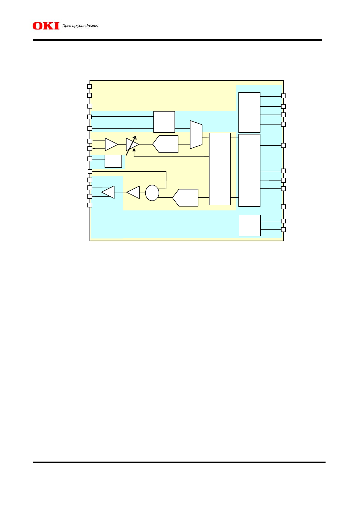
Block Diagram
LVDD
VMID
LGND
MDSCLKO(2612/6)
MDIN(2612/6)
MIN+(ML2612/4)
MIN-(ML2612/4)
MICBIAS
LIN
HVDD
SPOUT+
SPOUT-
HGND
BIAS
PGA
Digital
Mic I/F
+
ADC
DAC
SEL
ML2612 FAMILY DATASHEET
IFSEL(2612)
S3_SCLK/S2_SCLK
S3_SDATA/S2_SDATA
S3_CSB/MCLKO
SAI_SDOUT
SAI_SDIN
SAI_BCLK
SAI_LRCLK
RESETB(2612)
ALC
Prg
Filter
/
EQ
CPU
I/F
.
Audio
I/F
PLL
MCLKI
PLLC
Version: 3
5

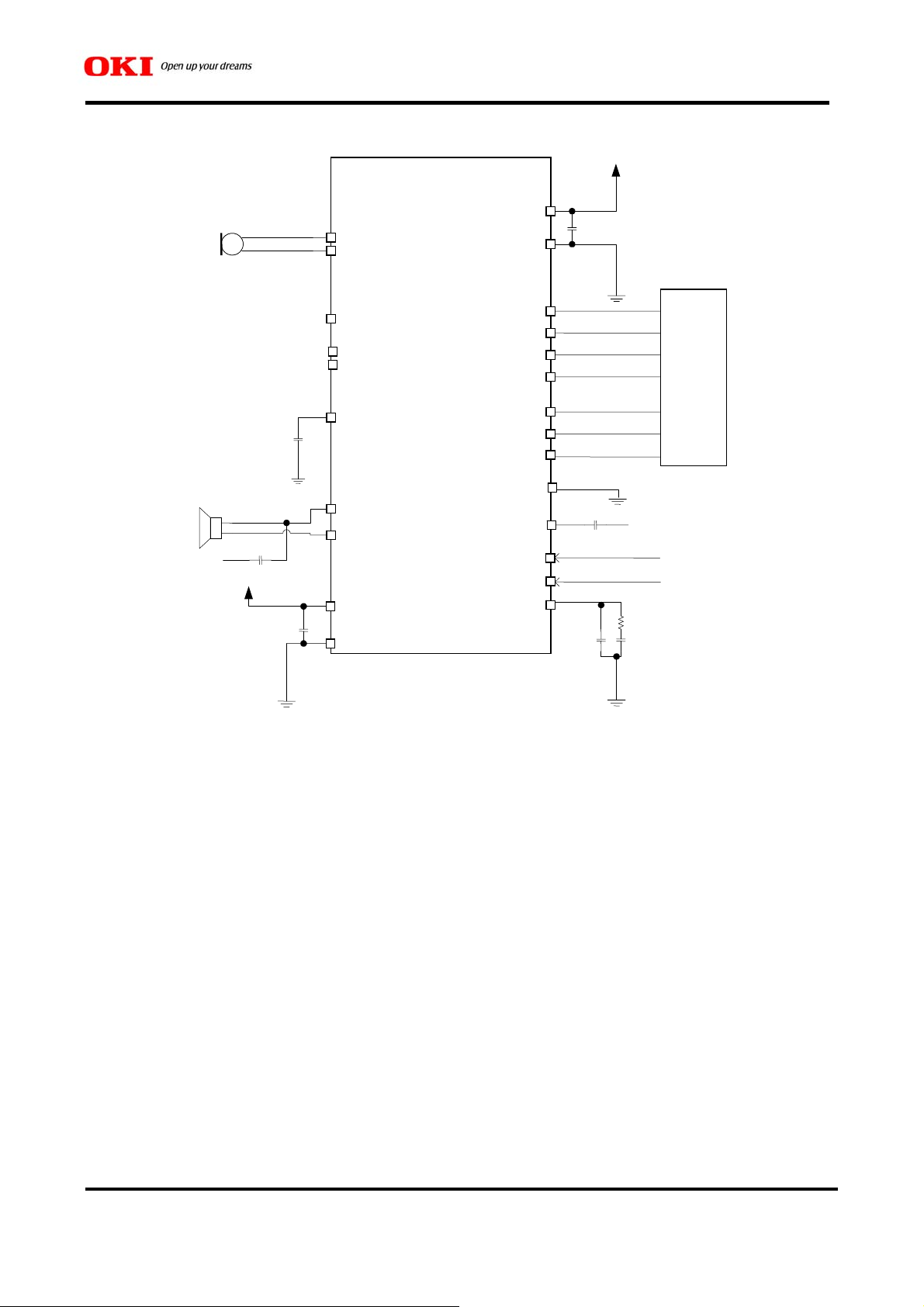
Application Example
open
ML2612
MDSCLKO
MDIN
LVDD
LGND
ML2612 FAMILY DATASHEET
MICBIAS
SAI_LRCLK
SAI_BCLK
MINMIN+
VMID
SAI_SDOUT
SAI_SDIN
S2_SDATA
CPU
DSP
S2_SCLK
MCLKO
SPOUT+
IFSEL
LIN Line In
(2-wire Select)
SPOUT-
RESETB
Line Out
HVDD
MCLKI
PLLC
HGND
Version: 3
6
●Application example for MEMS microphone with SDM
LVDD
LGND
SAI_LRCLK
SAI_BCLK
SAI_SDOUT
SAI_SDIN
S3_SDATA
S3_SCLK
S3_CSB
IFSEL
LIN
RESETB
MCLKI
PLLC
MEMS-MIC
with SDM
open
open
Line Out
ML2612
MDSCLKO
MDIN
MICBIAS
MIN+
MIN-
VMID
SPOUT+
SPOUT-
HVDD
HGND
ML2612 FAMILY DATASHEET
CPU
DSP
)
Line In
Version: 3
7
Pin Layout
ML2612GD (24Pin QFN)
Top View
ML2612 FAMILY DATASHEET
SAI_SDIN
S3_SDATA/S2_SDATA
LVDD
LGND
MDSCLKO
MIN+
SAI_SDOUT
S3_SCLK/S2_SCLK
IFSEL
RESETB
SAI_LRCLK
18 17 16 15 14 13
19
20
21
22
23
24
1 2 3 4 5 6
SAI_BCLK
MCLKI
12
S3_CSB/MCLKO
11
PLLC
10
MICBIAS
9
SPOUT-
8
SPOUT+
7
MIN-
VMID
LIN
HVDD
MDIN
HGND
Version: 3
8
ML2614HB (20Pin WCSP)
Bottom View
ML2612 FAMILY DATASHEET
SAI_SDIN S3_SCLK SAI_LRCLK MCLKI
S3_SDATA SAI_SDOUT SAI_BCLK PLLC
LVDD LIN S3_CSB MICBIAS
LGND MIN- HGND SPOUT-
MIN+ VMID HVDD SPOUT+
D C B A
ML2616HB (20Pin WCSP)
Bottom View
SAI_SDIN S3_SCLK SAI_LRCLK MCLKI
S3_SDATA SAI_SDOUT SAI_BCLK PLLC
LVDD LIN S3_CSB MICBIAS
LGND MDIN HGND SPOUT-
MDSCLKO VMID HVDD SPOUT+
5
4
3
2
1
5
4
3
2
1
D C B A
Version: 3
9

ML2612 FAMILY DATASHEET
Pin Description
Pin No.
QFN WCSP
Common terminals for all family products
8 A2 SPOUT- O HVDD Speaker – output Hi-Z Open
7 A1 SPOUT+ O HVDD Speaker + output Hi-Z Open
12 A5 MCLKI I HVDD Master clock input (input) 10 A4 PLLC O HVDD Capacitor and resistor connect pin for PLL stable
Pin Name IO Power Description Reset
state
HGND Open
operation. Please set following circuit near by pins as
possible.
PLLC pin
Unused
pin
3 C1 VMID O LVDD Capacitor connect pin for Analog reference voltage.
Please connect 1.0µF capacitor between this pin and
LGND.
9 A3 MICBIAS O HVDD Microphone bias voltage output. Please connect
2.2µF capacitor between this pin and HGND.
14 B5 SAI_LRCLK IO HVDD SAI LR clock input (input) 13 B4 SAI_BCLK IO HVDD SAI bit clock input/output (input) 19 D5 SAI_SDIN I HVDD SAI serial data input (input) 18 C4 SAI_SDOUT O HVDD SAI serial data output L 21 D3 LVDD P - Low voltage power supply.
Please connect bypass capacitor between this pin and
LGND.
22 D2 LGND P - Low voltage ground - -
5 B1 HVDD P - High voltage power supply.
Please connect bypass capacitor between this pin and
HGND.
6 B2 HGND P - High voltage ground - -
4 C3 LIN I LVDD Lin input Hi-Z Open
Terminals depends on product
ML2612GD has all terminals. Some pins are limited according with WCSP products.
2 C2 MIN- I LVDD Analog microphone - input
Apply for ML2612GD and ML2614HB
24 D1 MIN+ I LVDD Analog microphone + input
Apply for ML2612GD and ML2614HB
1 C2 MDIN I HVDD Digital microphone input
Apply for ML2612GD and ML2616HB
23 D1 MDSCLKO O HVDD Digital microphone data synchronous clock output
Apply for ML2612GD, and ML2616HB
16 N/A IFSEL I HVDD Control interface mode select
L: 3 wire serial interface H: 2 wire serial interface
Apply for ML2612GD
20 D4 S3_SDATA
/S2_SDATA
IO HVDD 3 or 2 wire serial interface data IO. When 3 wire
serial is selected, output interface becomes CMOS
type. When 2 wire serial is selected, output interface
becomes open drain type. Please use this pin with
external pull-up resister when 2 wire serial is
selected. If this pin is used with external pull-up
resistor, it possibly gets noise from power. Therefore
tamper noise design is required in the noisy
environment.
LGND -
HGND Open
- -
- -
Hi-Z Open
Hi-Z Open
(input) Open
L Open
(input) -
(input) -
Version: 3
10

17 C5 S3_SCLK
/S2_SCLK
I HVDD 3 or 2 wire serial interface clock IO. If this pin is
used with external pull-up resistor, it possibly gets
noise from power. Therefore tamper noise design is
required in the noisy environment.
11 B3 S3_CSB
/MCLKO
IO HVDD When IFSEL=L, chip select input for 3 wire serial
interface. When IFSEL=H,256fs clock output.
15 N/A RESETB I HVDD Active-low reset input.
Apply for ML2612GD
ML2612 FAMILY DATASHEET
(input) -
(input)/L
(input) -
-/ Open
Version: 3
11

ML2612 FAMILY DATASHEET
Absolute Maximum Ratings
Parameter Symbol Condition Rating Unit
LVDD Supply Voltage LVDD ― -0.3~3.5 V
HVDD Supply Voltage HVDD ― -0.3~4.5 V
Input Voltage Vin ―
Storage Temperature
Tstg ―
-0.3~VDD+0.3
-55~+125
V
°C
Power Dissipation*1
Output Current1
Output Current2
Note) Do not short the output pin to another output pin, power supply pin or GND pin.
(Output pin includes an IO pin which is in output mode)*1Please reffer to the.
Pd Ta=25°C 500 mW
IOSP SPOUT+/- pin -560~+560 mA
IOO Except SPOUT+/- -8 ~ +8 mA
Recommended Operating Condition
Parameter Symbol Condition Rating Unit
LVDD Supply Voltage LVDD
HVDD Supply Voltage HVDD
Operating Temperature
LVDD≦HVDD
LVDD≦HVDD
Top ― -20~+85 °C
1.65~2.75 V
2.7~3.6 V
Version: 3
12

ML2612 FAMILY DATASHEET
Electrical Characteristics
DC Characteristics
(LVDD=1.65~2.75V, HVDD=2.7~3.6V, Ta=-20~+85°C)
Parameter Symbol Condition Min. Typ. Max. Unit Related Pin
“H” Input Voltage VIH HGND=0V HVDD×0.8 ― VDD V
“L” Input Voltage
“H” Output Voltage
“L” Output Voltage 1
“L” Output Voltage2 VOL2
“H” Input leakage current IIH VIH=HVDD ― ― 10 µA
“L” Input leakage current IIL VIL=HGND -10 ― ― µA
Operating Current1
LVDD
Operating Current1
HVDD
Operating Current2
LVDD
Operating Current2
HVDD
Standby Current1 IDDS1 -20~25°C ― ― 5 µA
Standby Current2 IDDS2 -20~50°C ― ― 15 µA
Standby Current3 IDDS3 -20~85°C ― ― 75 µA
Note) Please reffer to the followingpage describing tpical current value.
Note) Standby current is total value for all power supply currents.
VIL HGND=0V 0 ― HVDD×0.2 V
VOH IOH=-1mA HVDD×0.85 ― ― V
VOL1 IOL=1mA ― ― HVDD×0.15 V
IOL=3mA,
HVDD>2V
HVDD<2V
IDDO1L ― ― 9 mA
IDDO1H
IDDO2L ― ― 13 mA
IDDO2H
Playback
no Load
Sin1kHz-Full
Scale output
Record
Sin1kHz-Full
Scale input
― ―
― ― 9 mA
― ― 6 mA
0.4
VDD×0.2
V
All Digital
Input
All Digital
Input
Except
S2_DATA
Except
S2_DATA
S2_DATA
All Digital
Input
All Digital
Input
Version: 3
13
ML2612 FAMILY DATASHEET
Power Consumption
The following table shows typical operating current under the following conditions
(LVDD=1.8V, HVDD=3.0V, Ta=25°C, no-load, no-signal, PLL off)
Operating Condition Symbol LVDD(mA) HVDD(mA) TOTAL(mW)
8ΩBTL Speaker playback (48kHz-Sampling)
Line output playback (48kHz-Sampling) IDDO2 2.1 1.4 7.98
Line input8ΩBTL speaker output(Clock stopped)
Line input Line output(Clock stopped) IDDO4 0.5 0.5 2.40
Analog Mic I/F recording (48kHz-Sampling) IDDO5 5.2 0.7 11.46
Digital Mic I/F recording(48kHz-Sampling) IDDO6 1.7 0.4 4.26
Note) MCLKI=12.288MHz(256fs), SAI – Master, 3wire Serial IF
Recording condition: ALC and HPF1 are enabled. HPF2 and 5band-Programmable Equalizer are disabled.
Playback condition: Playback Limiter and 5band-Programmable Equalizer are disabled.
Operating Condition Symbol LVDD(mA) HVDD(mA) TOTAL(mW)
8ΩBTL Speaker playback (48kHz-Sampling)
Line output playback(48kHz-Sampling) IDDO2 3.4 0.9 11.20
Line input8ΩBTL speaker output(Clock stopped)
Line input Line output(Clock stopped) IDDO4 0.8 0.5 3.50
Analog Mic I/F recording (48kHz-Sampling) IDDO5 7.4 0.7 20.60
Digital Mic I/F recording(48kHz-Sampling) IDDO6 2.4 0.4 7.20
Note) MCLKI=12.288MHz(256fs), SAI – Master, 3wire Serial IF
Recording condition: ALC and HPF1 are enabled. HPF2 and 5band-Programmable Equalizer are disabled.
Playback condition: Playback Limiter and 5band-Programmable Equalizer are disabled.
Operating Condition Symbol LVDD(mA) HVDD(mA) TOTAL(mW)
8ΩBTL Speaker playback (48kHz-Sampling)
Line output playback (48kHz-Sampling) IDDO2 2.7 2.4 12.06
Line input8ΩBTL speaker output(Clock stopped)
Line input Line output(Clock stopped) IDDO4 0.5 0.5 2.40
Analog Mic I/F recording (48kHz-Sampling) IDDO5 5.9 2.1 16.92
Digital Mic I/F recording(48kHz-Sampling) IDDO6 2.4 1.9 10.02
Note) MCLKI=27MHz, SAI – Master, 3wire Serial IF
Recording condition: ALC and HPF1 are enabled. HPF2 and 5band-Programmable Equalizer are disabled.
Playback condition: Playback Limiter and 5band-Programmable Equalizer are disabled.
Operating Condition Symbol LVDD(mA) HVDD(mA) TOTAL(mW)
8ΩBTL Speaker playback (48kHz-Sampling)
Line output playback(48kHz-Sampling) IDDO2 4.2 2.4 17.70
Line input8ΩBTL speaker output(Clock stopped)
Line input Line output(Clock stopped) IDDO4 0.8 0.5 3.50
Analog Mic I/F recording (48kHz-Sampling) IDDO5 8.2 2.1 26.80
Digital Mic I/F recording(48kHz-Sampling) IDDO6 3.2 2.9 13.70
Note) MCLKI=27MHz, SAI – Master, 3wire Serial IF
Recording condition: ALC and HPF1 are enabled. HPF2 and 5band-Programmable Equalizer are disabled.
Playback condition: Playback Limiter and 5band-Programmable Equalizer are disabled.
Standby Current typical value is follows
Parameter Symbol Condition Current value Unit
Standby Current1 IDDST1 25°C 1 µA
Standby Current2 IDDST2 50°C 3 µA
Standby Current3 IDDST3 85°C 15 µA
Note) Pop noise reduction bias resistor of SPOUT+ is off state
IDDO1 2.4 2.1 10.62
IDDO3 0.7 1.7 6.36
(LVDD=2.5V, HVDD=3.0V, Ta=25°C, no-load, no-signal, PLL off)
IDDO1 3.8 2.1 15.80
IDDO3 1.2 1.7 8.10
(LVDD=1.8V, HVDD=3.0V, Ta=25°C, no-load, no-signal, PLL on)
IDDO1 2.9 3.5 15.72
IDDO3 0.7 1.7 6.36
(LVDD=2.5V, HVDD=3.0V, Ta=25°C, no-load, no-signal, PLL on)
IDDO1 4.6 3.5 22.00
IDDO3 1.2 1.7 8.10
(LVDD=2.75V, HVDD=3.6V)
Version: 3
14

ML2612 FAMILY DATASHEET
AC Characteristics
Clock
PLL not used
(LVDD=1.65~2.75V, HVDD=2.7~3.6V, Ta=-20~+85°C)
Parameter Symbol Min Max. Unit
MCLKI Frequency fC 2.048 49.152 MHz
MCLKI Period tC 1/fC 1/fC ns
MCLKI “H” Length tCH tC*0.4 ― ns
MCLKI “L” Length tCL tC*0.4 ― ns
PLL used (SAI Master)
(LVDD=1.65~2.75V, HVDD=2.7~3.6V, Ta=-20~+85°C)
Parameter Symbol Min Max. Unit
MCLKI Frequency fC 11.2896 54 MHz
MCLKI Period tC 1/fC 1/fC ns
MCLKI “H” Length tCH
MCLKI “L” Length tCL
Note) SAI Slave can be operated without MCLKI input because internal clock is generated from SAI_LRCLK
tC*0.4
tC*0.4
― ns
― ns
Reset
MCLKI
t
, fC
C
tCH t
CL
(LVDD=1.65~2.75V, HVDD=2.7~3.6V, Ta=-20~+85°C)
Parameter Symbol Min Max. Unit
RESETB pulse width t
RESETB
5 ― µs
W_RST
t
WRST
Version: 3
15

2 wire serial interface
Parameter
ML2612 FAMILY DATASHEET
(LVDD=1.65~2.75V, HVDD=2.7~3.6V, Ta=-20~+85°C, CL=30pF)
Symbol
Standard mode Fast mode
Min Max. Min Max.
Unit
S2_SCLK Frequency
S2_SCLK "L" Length
S2_SCLK "H" Length
Hold time under Repeat [Start] Condition
Setup Time under Repeat[Start] Condition
Data Hold Time t
Data Setup Time t
Setup Time under [Stop] Condition
S2_SDATA
t
LOW
S2_SCLK
t
HD:STA
t
HD:DAT
t
SU:DAT
t
t
HD:STA
t
SU:STA
HD:DAT
SU:DAT
t
SU:STO
t
HIGH
f
SCL
t
LOW
HIGH
―
4.7
4.0
4.0 ― 0.6 ― µs
4.0 ― 0.6 ― µs
0
250
4.0 ― 0.6 ― µs
SU:STA
100
― 400 kHz
― 1.3 ― µs
― 0.6 ― µs
3.45 0 0.9 µs
― 100 ― ns
t
HD:STA
t
SU:STO
t
Version: 3
16

3 wire serial interface
Parameter Symbol Min Max. Unit
ML2612 FAMILY DATASHEET
(LVDD=1.65~2.75V, HVDD=2.7~3.6V, Ta=-20~+85°C, CL=30pF)
SCLK Low to Chip Select enable t
Chip Select enable to SCLK Low t
Chip Select enable to SCLK High t
SCLK High to Chip Select enable t
100 ― ns
SLCL
100 ― ns
CLSL
100 ― ns
CLSH
100 ― ns
SHCL
SCLK High Pulse Width tSH 50 ― ns
SCLK Low Pulse Width tSL 50 ― ns
Input Data Hold time t
Input Data Setup time t
SCLK last edge to Chip Select disable t
30 ― ns
IDH
30 ―
IDS
100 ― ns
CHS2
ns
Chip Select High Pulse Width tCH 100 ― ns
Output Data Valid t
― 40
ODV
ns
ns
Chip Select High to Data Transition t
― 40
CHDTS
Two kinds of timing is supported depends on the S3_SCLK pin level at data transfer start.Read or Write is
selected by LSB logic of INDEX.
S3_CSB
S3_SCLK
(Low start)
S3_SCLK
(High start)
S3_SDATA
t
SLCL
t
SHCL
t
CLSH
t
CLSL
123 4 5 6 7 8 9 10111213141516
t
t
SH
1 2 3 4 5 6 7 8 9 10111213141516
t
IDS
MSB LSB MSB LSB
t
IDH
t
SL
SL
t
SH
t
CHS2
Write(Input)
S3_SDATA
Read(Output)
INDEX Write data
MSB LSB
t
ODV
Read data
t
CHDTS
t
CH
Version: 3
17

SAI (Slave)
K
K
ML2612 FAMILY DATASHEET
(LVDD=1.65~2.75V, HVDD=2.7~3.6V, Ta=-20~+85°C, CL=30pF)
Parameter Symbol Min Max. Unit
*1t
SAI_BCLK Period t
SAI_BCLK “H” Length t
SAI_BCLK “L” Length t
SAI_LRCLK Hold Time t
SAI_LRCLK Setup Time t
SAI_SDOUT Delay Time t
SAI_SDIN Setup Time t
SAI_SDIN Hold Time t
is the delay time from later one of SAI_BCLK transition and SAI_LRCLK transition.
D_SDO
― 128fs Hz
C_BCLK
HW_BCLK
LW_BCLK
H_LRCLK
SU_LRCLK
D_SDO
73 ― ns
73 ― ns
20 ― ns
20 ― ns
*1
20 ― ns
SU_SDI
20 ― ns
H_SDI
―
SAI_LRCLK
t
SAI_BCLK
SAI_SDOUT
H_LRCLK
t
SU_LRCLK
HW_BCLK
t
C_BCLK
50 ns
t
LW_BCLK
t
SAI_LRCLK
SAI_BCLK
SAI_SDIN
t
D_SDO
t
SU_SDI
t
H_LRCL
SAI Transmit
t
H_SDI
SAI Receive
t
SU_LRCLK
t
HW_BCLK
C_BCL
t
LW_BCLK
t
Version: 3
18

SAI (Master)
K
ML2612 FAMILY DATASHEET
(LVDD=1.65~2.75V, HVDD=2.7~3.6V, Ta=-20~+85°C, CL=30pF)
Parameter Symbol Min Max. Unit
SAI_BCLK Period t
SAI_BCLK “H” Length t
SAI_BCLK “L” Length t
SAI_LRCLK Delay Time t
SAI_SDOUT Delay Time t
SAI_SDIN Setup Time t
SAI_SDIN Hold Time t
― 64fs Hz
C_BCLK
HW_BCLK
LW_BCLK
D_LRCLK
146 ― ns
146 ― ns
― 20 ns
― 20 ns
D_SDO
50 ― ns
SU_SDI
0 ― ns
H_SDI
SAI_LRCLK
t
C_BCLK
t
LW_BCLK
t
SAI_BCLK
SAI_SDOUT
t
D_LRCLK
HW_BCLK
SAI_LRCLK
SAI_BCLK
SAI_SDIN
t
D_SDO
t
D_LRCLK
t
SU_SDI
SAI Transmit
SAI Receive
t
C_BCL
t
H_SDI
HW_BCLK
t
LW_BCLK
t
Version: 3
19

Digital Microphone Interface
Parameter Symbol Min Max. Unit
ML2612 FAMILY DATASHEET
(LVDD=1.65~2.75V, HVDD=2.7~3.6V, Ta=-20~+85°C)
MDSCLKO Period t
MDSCLKO “H” Length t
MDSCLKO “L” Length t
MDIN Setup Time t
MDIN Hold Time t
C_MDSCLKO
HW_ MDSCLKO
LW_ MDSCLKO
SU_MDIN
H_MDIN
― 64fs Hz
146 ― ns
146 ― ns
50 ― ns
0 ― ns
ML2612GD and ML2616HB support 64fs 1 bit digital audio data transfer. Please input 1 bit digital audio data
synchronized with MDCLKO 64fs into MDIN.
MDSCLKO
MDIN
t
SU_MDIN
t
C_MDSCLKO
t
H_MDIN
LW_ MDSCLKO
t
HW_ MDSCLKO
t
Version: 3
20

r
y
ML2612 FAMILY DATASHEET
Power Supply Sequence
Please power on/off the LSI with all kind of power at the same time. Each power supply should power up/down in
50ms.Also keep all power supply in the ON state or the OFF state. Please avoide partial ON or partial OFF status.
All of the LSI circuit is initialized by power on reset when power on. To be a certain operation of Power On Reset,
Please start VDD level from 0V(GND level).
After power on, this LSI can be controled from the time passed Reset Time(t
All of the pins status are Hi-Z during Power On Reset.
Parameter Symbol Min Typ Max Unit
PON_RST
).
Power On Delay Time t
Power Off Delay Time t
Power Up Time t
Reset Time after Power On t
0 — 50 ms
VDD_ON
0 — 50 ms
VDD_OFF
— — 10 ms
VDD_UP
— — 150 ms
PON_RST
Powe
Suppl
Other
Power
Supply
PowerSupply*0.9
t
VDD_ON
PowerSupply*0.9
PowerSupply*0.1
PowerSupply*0.1
t
VDD_OFF
Version: 3
21

Higher voltage of 1.6V or
PowerSupply*0.9
ML2612 FAMILY DATASHEET
Power
Supply
0V
●ML2612 pin state
SAI_LRCLK/SAI_BCLK/
SAI_SDOUT/SAI_SDIN
S3_SDATA
●Host CPU internal state
●Host CPU pin state
S3_CSB
S3_SDATA
tVDD_UP
Inhibit register access
Unknown
Initialize
※1
※1
※1
Please shut dwn Pwer Supply from LSI power down
state.
There are no limitation for control timing and power
wave form.
tPON_RST
Software reset
Unknown Activate (depends on register setting)
Activate
After ML2612 power up it activates at “H” input to S3_CSB
Normal operation
After ML2612power up it output “H”
Software reset
It output “L” until ML2612 power is up.
Active
Power up control Control
Activate after software reset
SAI_SDOUT/SAI_LRCLK/
SAI_BCLK/SAI_SDIN
Active
※1 Input or PullUP or PullDown
Version: 3
22

ML2612 FAMILY DATASHEET
Analog Characteristics
The following specification is only guarantied when specification is optimized by using ML2612 family Trimming
Registers.
(LVDD=1.65~2.75V, HVDD=2.7~3.6V, Ta=-20~+85°C)
Parameter
Line Input
Full Scale Input Signal Level V
Input Resistance R
Mic Input
Full Scale Input Signal Level
(for ADC 0dB Input at 0dB Gain)
Input Resistance MIN- R
Input Resistance MIN+ R
Line OUT(SPOUT+, with 10kΩ /50pF load)
Full Scale Output Signal Level
(for 0dB Input at 0dB Gain)
Analog Reference Level(VMID-pin)
Analog Reference Voltage V
Microphone Bias(MICBIAS-pin)
Output Voltage
Vmic<HVDD*0.85
Output Current I
Symbol
V
V
LIN
LINFS
― 15 20 25
LIN
MINFS
Condition
MIN- ― ―
Min
Typ
― ―
MIN+ ― ―
PGA Volume = +35.25dB 0.6 1.5
MIN-
―
MIN+
PGA Volume = 0dB
PGA Volume = -12dB
―
―
66.3 88.4 111.5
44.2
70.7 88.4
LOUTFS
―
REF
V
MIC
MIC
DAC to Line OUT
Lin to Line OUT
IMIC =1mA, VBCON=0
Vmic<HVDD*0.85
IMIC =1mA, VBCON=1
Vmic<HVDD*0.85
IMIC =1mA, VBCON=2
Vmic<HVDD*0.85
IMIC =1mA, VBCON=3
Vmic<HVDD*0.85
IMIC =1mA, VBCON=4
Vmic<HVDD*0.85
IMIC =1mA, VBCON=5
Vmic<HVDD*0.85
IMIC =1mA, VBCON=6
Vmic<HVDD*0.85
IMIC =1mA, VBCON=7
Vmic<HVDD*0.85
―
0.591x
LVDD
0.667x
LVDD
0.90x
LVDD/2
1.12x
LVDD/2
1.21x
LVDD/2
1.44x
LVDD/2
1.48x
LVDD/2
1.66x
LVDD/2
1.84x
LVDD/2
2.20x
LVDD/2
2.52x
LVDD/2
― ― 2
0.695x
LVDD
0.785x
LVDD
LVDD/2
1.25x
LVDD/2
1.35x
LVDD/2
1.60x
LVDD/2
1.65x
LVDD/2
1.85x
LVDD/2
2.05x
LVDD/2
2.45x
LVDD/2
2.80x
LVDD/2
Max Unit
0.7x
LVDD
0.7x
LVDD
0.4
―
―
0.766x
LVDD
0.867x
LVDD
1.10x
LVDD/2
1.38x
LVDD/2
1.49x
LVDD/2
1.76x
LVDD/2
1.82x
LVDD/2
2.04x
LVDD/2
2.26x
LVDD/2
2.70x
LVDD/2
3.08x
LVDD/2
Vp-p
kΩ
Vp-p
Vp-p
kΩ
kΩ
kΩ
kΩ
Vp-p
Vp-p
V
V
V
V
V
V
V
V
V
mA
Version: 3
23

(LVDD=2.5V, HVDD=3.3V, Ta=25°C, 1kHz signal, fs=48kHz)
Parameter
Analog Inputs to ADC out
Signal to Noise Ratio SNR
Total Harmonic Distortion THD
Symbol
Condition
A-weighted
Speaker Amp Off *1
1kHz,input-3dBFS
Speaker Amp Off *1
LVDD on 100mVp-p,
Power Supply Rejection Ratio PSRR
10kHz noise,
no signal input
DAC to Line OUT(SPOUT+, with 10kΩ /50pF load)
Total Harmonic Distortion THD 1kHz,input 0dBFS
ML2612 FAMILY DATASHEET
Min
― 90 ―
― 86 ―
Typ
Max Unit
dB
dB
― 40 ― dB
― 60 ―
dB
Signal to Noise Ratio SNR A-weighted
HVDD on
100mV
Power Supply Rejection Ratio PSRR
100mV
,10kHz noise,
p-p
no signal input
LVDD on
,10kHz noise,
p-p
no signal input
DAC to Speaker OUT(SPOUT+/-, with 8Ω /50pF load )
Output Power Po THD=10%
Total Harmonic Distortion THD
Po=310mW,
1kHz signal
Signal to Noise Ratio SNR A-weighted
HVDD on
Power Supply Rejection Ratio PSRR
100mVp-p,10kHz noise
LVDD on
100mVp-p,10kHz noise
Microphone Bias(MICBIAS-pin)
Output Noise Voltage V
Power Supply Rejection Ratio PSRR
MICN
22Hz to 22kHz,
=1.6 x V
V
MIC
REF
HVDD on
100mVp-p,10kHz noise
*1 Speaker Amplifier Power Management Register($26h/$27h) SPCON = 00h
― 94 ―
― 50 ―
― 35 ―
dB
dB
dB
― 420 ― mW
― 40 ― dB
― 84 ― dB
― 60 ― dB
― 35 ― dB
― 8.2
― uV
― 60 ― dB
Version: 3
24

Digital Filter Characteristics
Parameter
ADC Decimation Filter
Passband
Passband Ripple DM
Stopband DM
Stopband Attenuation DM
Group Delay DM
ADC High Pass Filter 1 (DC-Cut)
Corner Frequency
DAC Interpolation Filter
Passband
Passband Ripple IT
Stopband IT
Stopband Attenuation IT
Group Delay IT
Note) HP1f1, HP1f2 and HP1f3 are in proportion to fs
Symbol
DM
DM
+/-0.05dB
PS1
-6dB
PS2
lp1
st1
0.5465fs<Freq
at1
gd1
HP1f1 -3dB, fs=48kHz
HP1f2 -0.5dB, fs=48kHz
HP1
-0.1dB, fs=48kHz
f3
IT
+/-0.03dB
PS1
-6dB
IT
PS2
lp1
st1
0.5488fs<Freq
at1
gd1
Condition
ML2612 FAMILY DATASHEET
Min Typ Max Unit
0
―
-0.05
0.5465fs
-56 dB
―
―
―
―
0
―
-0.03
0.5488fs
-54 dB
―
―
0.5fs
―
20fs
3.744
10.656
24.192
―
0.5fs
―
18fs
0.455fs
―
+0.05 dB
―
―
―
―
0.452fs
―
+0.03 dB
―
―
―
―
―
Hz
Hz
Hz
―
―
―
―
Version: 3
25

ML2612 FAMILY DATASHEET
Revision history
Date Page Notes Notes RevisionRevision
07/05/15 All Preliminary datasheet Release 1.0
07/06/19 All Delete ML2613 and ML2615 1.2
07/06/19 3 Add Sampling Frequency 12kHz 1.2
07/06/19 14 Change Power Consumption value 1.2
07/06/19 18 Add t
07/06/19 21 Change Power up time MAX value 1.2
07/06/19 23 Change Analog Characteristics condition and value 1.2
07/09/07 12 Absoute Maximum Rating: Delete (T.B.D.) for Powwer Disipation and
add Output Current.
07/09/07 13 Change operating current value amd delete (T.B.D.) 2
07/09/07 15 Change MCLKI Length Min value 2
07/09/07 21 Change Pwer Up Time and Reset Time after Power On 2
07/09/07 22 Change Power Supply Sequence 2
07/09/07 23 Change Analog Characteristics 2
07/09/07 25
07/10/31 3 Change General Description 3
07/10/31 23 Change Analog Characteristics(RMIN+, VLOUTFS) 3
Digital Filter Characteristics: Change value and delete (T.B.D.)
Condition 1.2
D_SDO
2
2
Version: 3
26

ML2612 FAMILY DATASHEET
NOTICE
1. The information contained herein can change without notice owing to product and/or technical improvements.
Before using the product, please make sure that the information being referred to is up-to-date.
2. The outline of action and examples for application circuits described herein have been chosen as an
explanation for the standard action and performance of the product. When planning to use the product, please
ensure that the external conditions are reflected in the actual circuit, assembly, and program designs.
3. When designing your product, please use our product below the specified maximum ratings and within the
specified operating ranges including, but not limited to, operating voltage, power dissipation, and operating
temperature.
4. Oki assumes no responsibility or liability whatsoever for any failure or unusual or unexpected operation
resulting from misuse, neglect, improper installation, repair, alteration or accident, improper handling, or
unusual physical or electrical stress including, but not limited to, exposure to parameters beyond the
specified maximum ratings or operation outside the specified operating range.
5. Neither indemnity against nor license of a third party’s industrial and intellectual property right, etc. is
granted by us in connection with the use of the product and/or the information and drawings contained herein.
No responsibility is assumed by us for any infringement of a third party’s right which may result from the
use thereof.
6. The products listed in this document are intended for use in general electronics equipment for commercial
applications (e.g., office automation, communication equipment, measurement equipment, consumer
electronics, etc.). These products are not authorized for use in any system or application that requires special
or enhanced quality and reliability characteristics nor in any system or application where the failure of such
system or application may result in the loss or damage of property, or death or injury to humans.
Such applications include, but are not limited to, traffic and automotive equipment, safety devices, aerospace
equipment, nuclear power control, medical equipment, and life-support systems.
7. Certain products in this document may need government approval before they can be exported to particular
countries. The purchaser assumes the responsibility of determining the legality of export of these products
and will take appropriate and necessary steps at their own expense for these.
8. No part of the contents contained herein may be reprinted or reproduced without our prior permission.
Version: 3
Copyright 2006 Oki Electric Industry Co., Ltd.
27
 Loading...