

Page 1

OKIPAGE8
p
LED Page Printer
Troubleshooting Manual
with Component Parts List
(ODA/OEL/INT)
All specifications are subject to change without notice.
Page 2

CONTENTS
1. OUTLINE..................................................................................................... 1
2. TOOLS........................................................................................................ 1
3. CIRCUIT DESCRIPTION............................................................................ 2
3.1 Outline ..................................................................................................................... 2
3.2 CPU and Memory .................................................................................................... 4
3.3 Reset Control........................................................................................................... 6
3.4 EEPROM Control..................................................................................................... 7
3.5 Centronics Parallel Interface.................................................................................... 8
3.6 Front Operator Panel ............................................................................................... 9
3.7 LED Head Control ................................................................................................. 10
3.8 Motor and clutch control ........................................................................................ 12
3.9 Fuser Temperature Control.................................................................................... 14
3.10 Sensor Control....................................................................................................... 17
3.11 Cover Open ........................................................................................................... 18
3.12 Power Supply Part ................................................................................................. 19
4. TROUBLESHOOTING.............................................................................. 21
4.1 Troubleshooting T able ............................................................................................ 21
4.2 Troubleshooting Flowchart..................................................................................... 23
5. CIRCUIT DIAGRAM.................................................................................. 27
6. COMPONENT PARTS LIST
Page 3
1. OUTLINE
This manual has been written to provide guidance for troubleshooting of the OKIPAGE8p Printer
(primarily for its printed circuit boards), on an assumption that the reader is knowledgeable of the
printer. Read the maintenance manual for this printer if necessary.
Note:
1. High voltage power supply board and power supply unit containing a high voltage power
supply is dangerous. From the viewpoint of the safety standards, the local repairing of a
defective board is not allowed. Thus, the objects to be locally repaired as a result of
troubleshooting are switches.
2. TOOLS
For troubleshooting the printer, the tools listed below may be needed in addition to general
maintenance tools.
Oscilloscope Frequency response 100 MHz or higher
Soldering iron A slender tip type, 15-20 watts
Tool Remarks
- 1 -
Page 4

3. CIRCUIT DESCRIPTION
3.1 Outline
The circuit of OKIPAGE8p consists of a main control board, a main high voltage power supply
board, a sub-high voltage power supply board and a power supply unit. The block diagram is
shown in Fig. 3-1. The main control board controls the reception and transmission of data with
a host I/f and processes command analysis, bit image development, raster buffer read. It also
controls the engine and high voltage outputs.
(1) Reception control
The main control board has one parallel I/F port which is compliant to the IEEE 1284
specification.
The parallel I/F port can specify the following item when set by the control panel:
I-PRIME: Enabled/ Disabled
(2) Command analysis processing
The OKIPAGE8p printers support PCL5e (Hewlett Packard LJ6P compatible).
An edit task fetches data from the receive buffer, analizes commands, and reconstructs the
data in such a way that print data are aligned from up to down and from right to left; then it
writes the resultant data into a page buffer with such control data as print position coordinate,
font type, etc. added.
(3) Font Processing
When one page editing is finished, a developing task makes an engine start and fetches data
from the page buffer synchronizing with a printing operation; then it developes the fetched
data to a bit map as referring to data from a character generator, and writes the resultant data
into the raster buffer (of band buffer structure).
(4) Raster buffer read
As controlling the engine operation, an engine task sends data from the raster buffer to the
LED head.
(5) High voltage control (main, sub)
The high voltage control circuit in the CPU.
The high voltage power supply board generates high voltage outputs, and have sensors, LED for
display.
The power supply unit generates +26VDC output, +5DC output.
- 2 -
Page 5

PLUNGER LED HEAD
Motor
M
- 3 -
HEAD2HEAD1PJ
Figure 3-1 OKIPAGE8p Block Diagram
Parallel
I/F
CENT
LS07
+5V+26V
POWER
MOTOR Main PCB NMA-
0V5V
0VP0V
Motor Driver
MTD2005F
CPU
(NKK3 or 5)
Data Bus
Address Bus
OSC
7MHz
RST
EEPROM
Serial I/F
(x16)
LC26023A
1kb
OSC
10MHz
LSI
HIVOL
DRAM 2MB
M-ROM
4M x 16
Mask ROM 8MB
HC244
HIVOL2
Red
Amber
Amber
DRAM
1M x 16
0V
OPTION
O
P
T
I
O
N
PCB N4A-
DRAM
1M x 16
DRAM 4MB
Power Supply Unit
AC
(120V/ 230V)
Heater
(Halogen lamp)
High Voltage Power Unit
P2H
High Voltage Power Unit
P6L
ID Unit
Page 6

3.2 CPU and Memory
(1) CPU (NKK3 or NKK5)
CPU core RISC CPU (MIPS R3000)
CPU clock 7.067 MHz, Internal CPU CLK 28.268 MHz
Data bus width External 16 bits, Internal 32 bits
(2) Program ROM
ROM capacity 8M-bytes (Mask ROM)
ROM type 64Mbits (4M x 16 bits)
Access time 100 nsec
(3) Resident RAM
RAM capacity 2M bytes (1Mx 16 bits)
RAM type 16M bits (1M x 16 bits)
Access time 60 ns
(4) Option Board
RAM capacity 4M bytes (16M bits D-RAM two pieces)
RAM type 16M bits D-RAM two pieces
Access time 60 n
The block diagram of CPU and memory circuit is shown in Fig. 3-2.
- 4 -
Page 7

CPU
CS0
RAS0
RAS1
RAS2
A00 to A25
D00 to D15
CS0
Mask ROM
(4M x 16 bits)
<Program>
RD
CAS0
CAS1
RAS0
RD/WR
CAS0, 1
RAS1, 2CAS0, 1 WR
RAS1, 2 WR
CAS0,1
DRAM
(1M x 16 bits)
Main
control
board
Option
board
DRAM
4M Byte
Figure 3-2 Block Diagram of CPU & Memory in OKIPAGE8p
- 5 -
Page 8
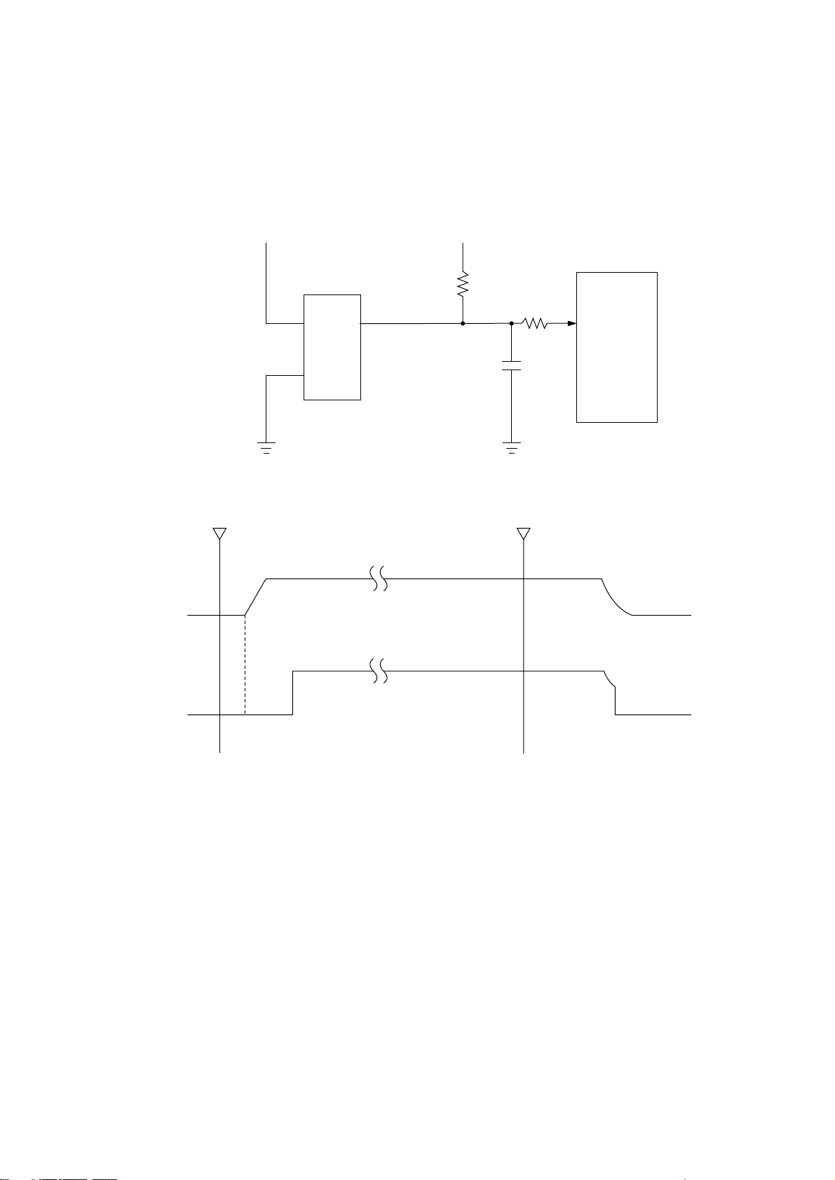
3.3 Reset Control
When power is turned on, RST-N signal is generated by RST.
+5V+5V
+5V
Power ON
RST
1
3
2
Power OFF
172
CPU
RSTN
CL RST-N
- 6 -
Page 9
3.4 EEPROM Control
The BR93LC46A on the main control board is an electrical erasable/programmable ROM of 64bit x 16-bit configuration. Data input to and output from the ROM are bidirectionally transferred
in units of 16 bits through I/O port (EEPRMDT-P) in serial transmission synchronized with a clock
signal from the CPU.
The EEPROM operates in the following instruction modes.
Instruction Start bit Operation Address Data
Read (READ) 1 10 A5 to A0
Write Enabled (WEN) 1 00 11XXXX
Write (WRITE) 1 01 A5 to A0 D15 to D0
CPU
154
150
151
SSTXD-P
EEPRMCSO-P
EEPRMCLK-P
code
3
DI DO
EEPROM
1
CS
IC4
4
SK
2
CS
SK
DI
CS
SK
DI
DO
Write All Address (WRAL) 1 00 01XXXX D15 to D0
Write Disabled (WDS) 1 00 00XXXX
Erase 1 11 A5 to A0
Chip Erasable (ERAL) 1 00 10XXXX
Write cycle timing (WRITE)
1 2 4 9 10 25
10 1
HIGH-Z
A5 A4 A1 A0 D15
D14
D1 D0
Min. 450 ns
STATUS
Max. 500 ns
BUSY READY
Max. 10 ms
Read cycle timing (READ)
12
110
4
A5 A4 A1 A0
910
25 26
DO
HIGH-Z
D15 D14 D1 D00 D15 D14
- 7 -
Page 10
3.5 Centronics Parallel Interface
The CPU sets a BUSY-P signal to ON at the same time when it reads the parallel data (PDATA1P to PDATA 8-P) from the parallel port at the fall of PSTB-N signal. Furthermore, it makes the store
processing of received data into a receive buffer terminate within a certain fixed time and outputs
an ACK-N signal, setting the BUSY-P signal to OFF.
87, 88, 91 to 96
97
85
86
CPU
83
81
79
80
82
84
PDATA1-P to PDATA8-P
PSTB-N
Q4
PBUSY-P
PACK-N
PRE-P
PSEL-P
PERROR-P
PINIT-N
PSELIN-N
PALITOFD-N
2 to 9
1
11
10
12
13
32
31
36
14
CENT
DATA8-P
to
DATA1-P
STB-N
BUSY-P
ACK-N
PE-P
SEL-P
FAULT-N
IPRIME-N
SELIN-N
AUTOFEED-N
PARALLEL DATA
(DATA BITs 1 to 8)
DATA STOROBE
BUSY
ACKNOWLEDGE
0.5 µs min.
0.5 µs min.
0.5 µs max.
0 min.
0.5 µs to 10 µs
+5V+5V or High Level
18
0.5 µs min.
0.5 µs min.
0 min.
0 min.
0 min.
- 8 -
Page 11
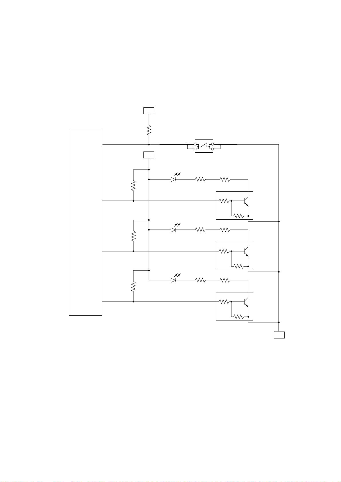
3.6 Front Operator Panel
Front operator panel have three LED lamps and a switch on the main control board which is
connected to by the CPU.
The light from the LED lamp can be seen on the Lens Cover through the LED Lens.
5V
CPU
110
5V
Ready (Amber)
114
Manual Feed (Amber)
113
Error (Red)
161
- 9 -
0V
Page 12

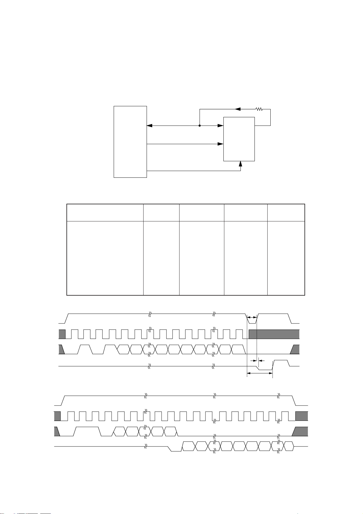
3.7 LED Head Control
An LED correcting head, which is capable of correcting the illumination of the LED for each dot,
is being used in this printer. LED illumination correction function of 16 steps is carried out by using
an EEPROM which is installed in the LSI that maintains the LED illumination correction values,
and an LED correction drivers (MSM6731BWAF or MSM6732BWAF) together as a pair.
The LED correcting head consists of the correction control LSI (MSM6730WAF), LED drivers
(MSM6731BWAF or MSM6732BWAF), and an LED array.
From
CPU
STRB1-N
STRB2-N
STRB3-N
STRB4-N
LOADI
CLOCKI
DATAI0
DATAI1
DATAI2
DATAI3
MSM6730
WAF
EEPROM
Correction
Values
LED Driver
MSM6732BWAF
LED Array
LED LED LED LED LED LED LED
LED Driver
MSM6731BWAF
Printing and correction data combined signal line
Correction data signal line
LED Driver
MSM6731BWAF
LED Driver
MSM6732BWAF
- 10 -
Page 13
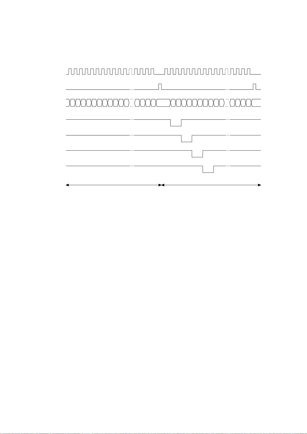
CLOCKI
LOADI
DATAI3~0
STRB1I-N
STRB2I-N
STRB3I-N
STRB4I-N
Normal Mode Printing Timing Chart
First line printing data sent Second line printing data sent
First line printing
The printing operation is carried out in the following sequence. First, the printing data DATAI3
through DATAI0 are stored, sequentially shifted, in the shift registers of the LED drivers, by the
printing data synchronous clock, CLOCKI. Then the printing data stored in shift registers are
latched by the high level pulse of LOADI. The latched printing data turns the LEDs on by STRB1IN through STRB4I-N and actuates printing.
- 11 -
Page 14
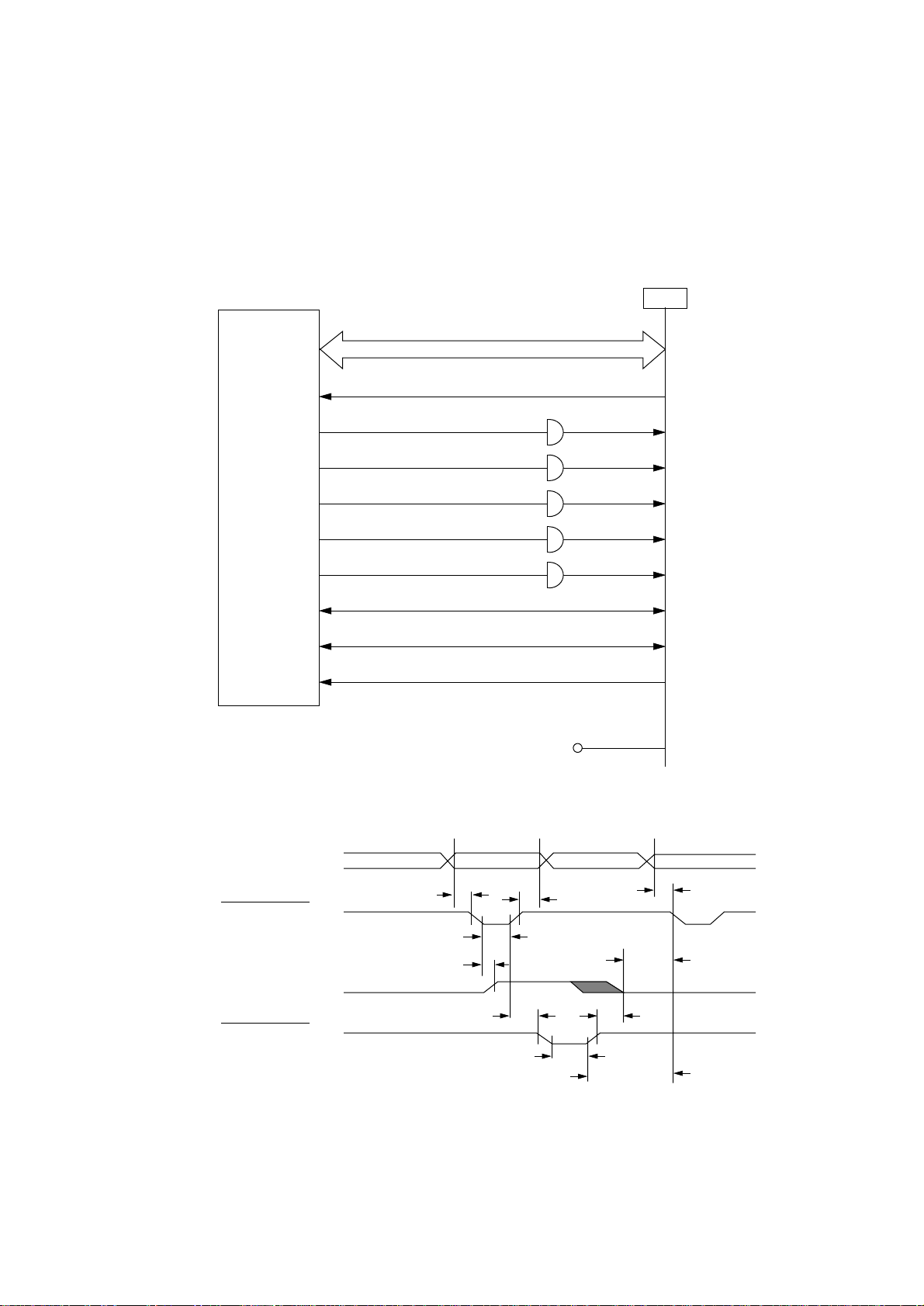
3.8 Motor and clutch control
The electromagnetic clutch is driven by a control signal from the CPU and the drive circuit shown
below.
The main motor is driven by the control signals from the CPU and the driver IC.
CPU
DMON1N
DMPH1P
DMPH2P
127
132
131
MTDV
+5V
+5V
ENA A
27
To Out3, 4Logic
18
DECAY
26
PHASE A PHASE B
Motor
19
Out1
SW1 SW3
GATE CIRCUIT
M
Main Motor
+26V OPEN
37 1 1412 24
Out2 Out3
8
Out4Vmm A Vmm B
ALARM
120°C 140°C
ENA B
SW1 SW3
GATE CIRCUIT
Signal of
DECACY
16
17
+5V +26V
RMONN
128
(1) Main motor
+5V
+5V
0V
25
BRUNK
0V
0V
SW4SW2
Current
Q
-
R
+
S
Sensor
OSC
Vref A Vref B
Vs A Vs BRs A Rs BLG A PG LG B
23 22 28 15 10 21 20TAB5
PJ
Electromagnetic clutch
0VP
0V
SW4SW2
Current
Sensor
RQ
+
S
DMON-P
DMPH1-P
DMPH2-P
Rotation
T0 T1 T2 T3
Forward rotation
Reverse rotationStop
Operation at normal speed: T0 to T3 = 0.781 ms
- 12 -
Page 15
(2) Motor drive control
Time T0 to T3 determines the motor speed, while the phase different direction between
phase signals DMPH1-P and DMPH2-P determines the rotation direction. DMON-N signal
control a motor coil current. According to the polarity of the phase signal, the coil current flow
as follows:
1) +26V → SW1 → motor coil → SW4 → resistor → earth
2) +26V → SW3 → motor coil → SW2 → resistor → earth
The drop voltage across the resistor is input to comparator, where it is compared with a
reference voltage. If an overcurrent flows, a limiter operates to maintain it within a certain
fixed current.
(3) Electromagnetic clutch control
Mechanical operation mode is switched by the combination of the clutch status and the
direction of motor rotation.
clutch status
off
off
on
on
rotation direction
Forward
Reverse
Forward
Reverse
operation mode
cleaning
Hopping from manual
feed slot
illegal operation
Hopping from tray
- 13 -
Page 16
3.9 Fuser Temperature Control
For the temperature control by heater control, the variation in the resistance of the thermistor is
A/D converted in LSI and the resultant digital value is read and transferred to the CPU. The CPU
turns on or off the HTON-N signal according to the value of the signal received from LSI to keep
the temperature at a constant level.
Immediately after the power is turned on, the thermistor is checked for shortcircuit and
breakdown. If the thermistor is shorted, the A/D converted value shows an abnormally high
temperature, so that the shortcircuit can be detected. If the breakdown of the thermistor occurs,
the A/D converted value shows the normal temperature. In this case, the thermistor breakdown
can be detected by the sequence shown at the end of this section. If the heater is overheated,
5V supply is turned off when the resistance of the thermistor is detected to be exceeding the
predetermined value.
Main Control BoardHigh Voltage Power Supply Board
CN2
Thermistor
Heater
TH1
TH2
5V
Power Supply Unit
CN1
1
2 PC1
5V
36
8
ACIN
LSI CPU
Abnormally
High
Temperature
Detection
Circuit
HTON
116
Shutdown
5V
Circuit
Q3
0C
5V
13
Q3
0C
14
- 14 -
Page 17
Flowchart of Thermistor Circuit Check
START
HEATER OFF
Short check timer(t16)set
No
Time-out ?
Short error TEMP ?
Thermistor error check
timer (t2) set
Thermistor disconnection
check timer (t35) set
Heater On
Temperature > Tn
Thermistor
error check timer (t2)
within time
No
No
Yes
Yes
Yes
Thermistor short error
End
Yes
To constant
temperature control
No
Fuser error
Thermistor
disconnection check timer
(t35) within time
Yes
t2 =
90 sec
t16 =
520 msec
t35 =
10 sec
No
A/D value changed?
Yes
Thermistor
disconnection error
End
- 15 -
No
Thermistor gain change
(THERMCMP-N"0" "Z")
No
A/D value more than
End
20H?
Yes
Fuser error
End
Page 18

Temperature
Controlled
Temperature
T
HEATER ON
OFF
Time
Temperature table
THERMCMP-N
O
Z
T
145˚C:
150˚C:
155˚C:
160˚C:
165˚C:
Heater control mode
Normal operation
Fuser Error Check
Paper Thickness
light
medium light
medium
medium heavy
heavy
- 16 -
Page 19

3.10 Sensor Control
The CPU supervises the state of each sensor every 40 ms.
Main Control Board High Voltage Power Supply Board
HIVOL CN1
+5V
CPU
Sensor
signal
124
120
122
123
OFF
+5V
+5V
+5V
+5V
TNRSNS-N
PSIN-N
PSOUT-N
WRSNS-N
TransparentShield
PS1
PS2
PS3
PS4
ON
- 17 -
Page 20
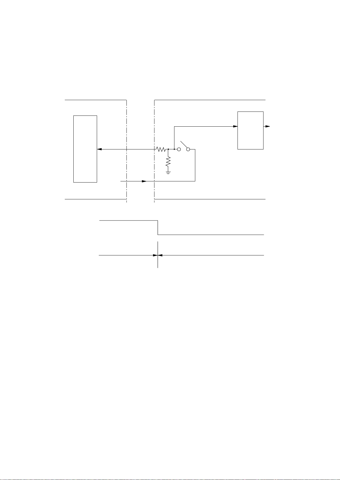
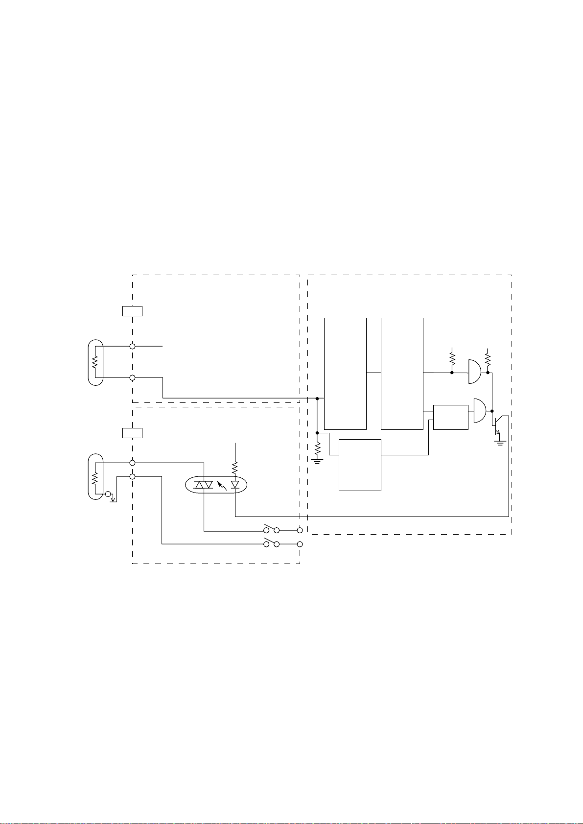
3.11 Cover Open
When the cover is opened, a cover open microswitch is opened. This makes a CVOPN-N signal
low, thereby the CPU detects that cover is open. Furthermore, opening the cover stops applying
a +5V power to the high voltage power supply part, resulting in stopping all high voltage outputs.
HIVOL CN1
Main Control Board
CVOPN-N
CPU
+5V
0V
125
Cover close Cover open
CVOPN-N
Cover
Open
Microswitch
+5V
High Voltage Power Supply Board
High
Voltage
Power
Supply
+5V
Part
High
voltage
output
- 18 -
Page 21

3.12 Power Supply Part
(1) Power supply unit
An AC power from an inlet is input to Switching Reg. part .AC power is converted to a +26
VDC output and +5 VDC output.
ACIN
F1 F2L
FG
N
Filter
Circuit
Power supply unit
+26V
+5V
0V
HEATER
Switching Reg. Part
CONTROLER
HEATON-N
to AC output
Fuse Ratings
AC Input
Fuse
F1
F2
230 V
250 V 6.3 A
250 V 2 A
120 V
125 V 8 A
250 V 2.5 A
(2) High voltage power supply board
The +5 VDC power supplied to the high voltage power supply part via the cover open
microswitch as source voltage. The high voltage power supply part supplies necessary
voltage for electro-photography print to output terminals CH, DB, SB, TR, and CB according
to a control signal from the LSI. The table on the next page shows the relationship between
control signals and high voltage outputs.
HIVOL
MainControl Board High Voltage Power Supply Board
TR1PWM
11
TR2PWM
12
CHPWM
13
DB1ENB-P
24
LSI
23
14
15
16
3
DB2ENB-P
DBPWM
CVOPN-N
+5V
CB2PWM
CB1PWM
CN1
P2H
High Voltage
Power Supply
Part
P6L
CH
DB
SB
TR
Cover Open
Microswitch
CB
- 19 -
Page 22

Control Signals and High Voltage Outputs
Control signal name Level Function
TR1PWM
TR2PWM
CHPWM
DB1ENB-P
DB2ENB-P
DBPWM-P
CB1PWM
H/L
(PWM)
L
H/L(PWM)
L
H/L(PWM)
L
H
L
H
L
H/L(PWM)
L
H/L(PWM)
L
Makes the part put out a power to TR.
+3 to 5 µA
+0.5 to 4 KV
Makes the part put out a -750V power to TR.
Makes the part put out a -1300 KV power to CH.
Makes the part put out the following power:
0V power to SB
+265V power to DB
Makes the part put out the following power:
-550V power to SB
-265V power to DB
Makes the part put out the power to SB, DB, CB.
Makes the part put out a
+400V to CB
CB2PWM
H/L(PWM)
L
Makes the part put out a -1350V to CB
- 20 -
Page 23

4. TROUBLESHOOTING
4.1 Troubleshooting Table
(A) High Voltage Power Supply Board
Note:
A malfunction of the power supply is not repaired by an agency. The abnormality to be
treated here is that of sensors only.
Failure
A paper input jams occur
frequently.
A paper feed jams occur
frequently.
A paper-exit jams occur
frequently.
A paper size errors occur
frequently.
Paper can not be fed from the
manual feed slot .
The message "COVER OPEN"
remains displayed on the PC
display.
Error(RED)
Flash2
Flash2
Flash2
Flash2
off
LED
Manual Feed
(amber)
off
off
off
off
Undefined
Ready
(amber)
off
off
off
off
off
PC Display Message
PAPER
INPUT JAM
PAPER
FEED JAM
PAPER
EXIT JAM
PAPER
SIZE ERROR
COVER OPEN
Flowchart
No.
A - 1
A - 2
A - 3
A - 4
A - 5
A - 6
The message "TONERLOW"
remains displayed on the PC
display.
The message "TONERSNS"
remains displayed on the PC
display.
Flash2 : Blinking
Flash3 : Fast Blinking
Flash2
off
Undefined
Undefined
- 21 -
Undefined
Undefined A - 8
TONER LOW
TONER SENSOR
A - 7
PROBLEM
Page 24

(B) Main Control Board
LED
Failure
Initialization error
and not restored
Program ROM
error
Resident RAM
error
EEPROM error B - 4
Fuser error Flash3 B - 5
Thermister Open
error
Error(RED)
Flash3
Flash3
Flash3
Flash3
Manual Feed
(amber)
Flash3
Flash3
Flash3
Flash3
Flash3
Ready
(amber)
Flash3
Flash3
Flash3
Flash3
Flash3
PC Display Message
ERROR 10
ERROR 30
ERROR 40
ERROR 71
ERROR 72
Flowchart
No.
B - 1
B - 2
B - 3
B - 5
Thermister Short
error
Watchdog timer
timeout occurs
frequently.
Data sent through the
Parallel I/F cannot be
received.
Flash2 : Blinking
Flash3 : Fast Blinking
Flash3
Flash2 B - 6
Flash3
Flash2
Flash3
Flash3
Flash2
Flash3
ERROR 73
ERROR 90
CONNECTION PROBLEM
B - 5
B- 7Flash3
- 22 -
Page 25

4.2 Troubleshooting Flowchart
A-1 Paper input jams occur frequently.
• Is PS4 (Write Sensor ) operating normally?
• No Replace PS4.
▼
• Yes Is Pin1 of PJ connector in main control board operating normally?
• No Replace TR501 or TR502 in main control board.
▼
• Yes Failure of CPU in main control board.
A-2 A paper feed jams occur frequently.
• Is PS4 (Write Sensor ) operating normally?
• No Replace PS4.
▼
• Yes Is PS3 (Outlet Sensor ) operating normally?
• No Replace PS3.
▼
• Yes Failure of CPU in main control board.
A-3 A paper exit jams occur frequently.
• Is PS3 (Outlet Sensor) operating normally?
• No Replace PS3.
▼
• Yes Failure of CPU in main control board.
A-4 A paper size errors occur frequently.
• Is PS4 (Write Sensor ) operating normally?
• No Replace PS4.
▼
• Yes Failure of CPU in main control board.
A-5 Paper can not be fed from manual feed slot.
• Is PS2 (Manual Feed Sensor) operating normally?
• No Replace PS2.
▼
• Yes Failure of CPU in main control board.
- 23 -
Page 26

A-6 The message “COVER OPEN” remains displayed on the PC display.
• Is CVSW (Cover Open Switch) operating normally?
• No Replace CVSW.
▼
• Yes Failure of CPU in main control board.
A-7 The message “TONERLOW” remains displayed on the PC display.
• Is PS1 (Toner Sensor) operating normally?
• No Replace PS1.
▼
• Yes Failure of CPU in main control board.
A-8 The message “TONERSNS” remains displayed on the PC display.
• Is PS1 (Toner Sensor) operating normally?
• No Replace PS1.
▼
• Yes Failure of CPU in main control board.
- 24 -
Page 27

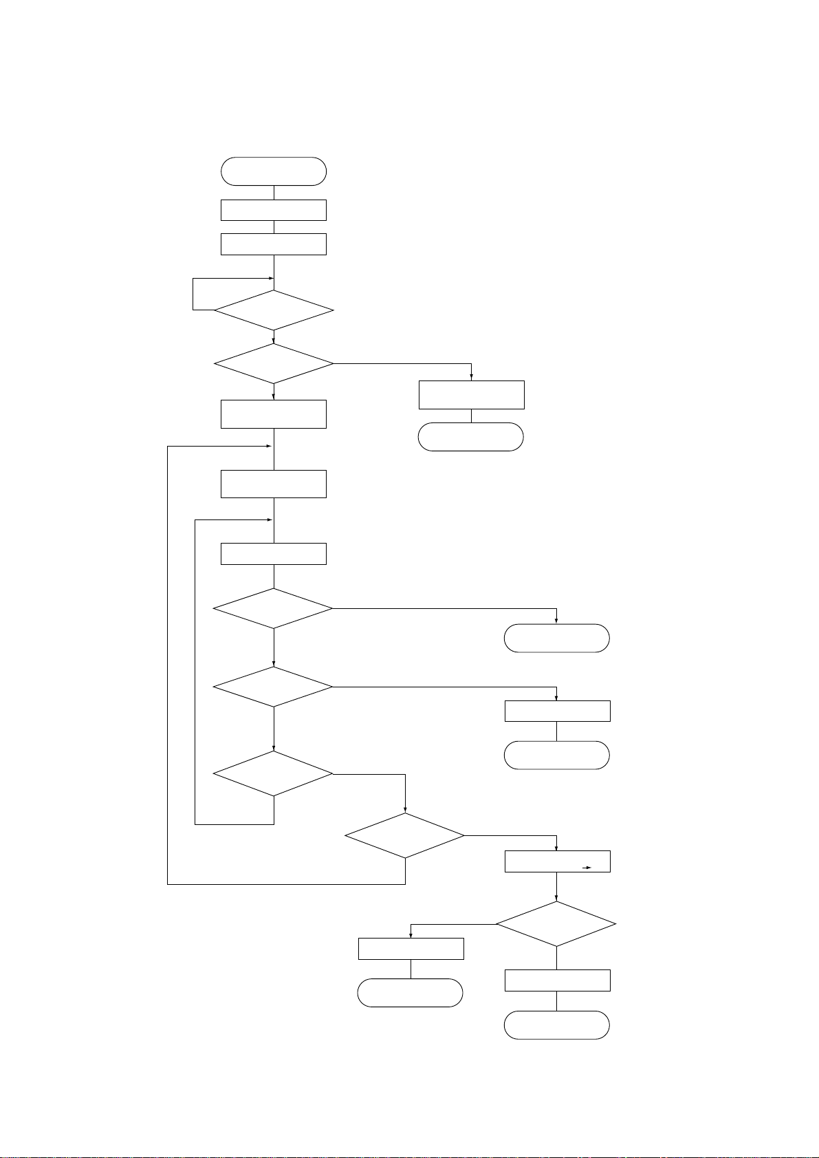
B-1 Initialization error and not restored
• Replace ROM.
▼
• OK?
▼
• No Is the 7.065-MHz clock signal being put out to pin 3 of OCS1?
• No Replace OSC1 (CST 7.065M).
▼
• Yes Failure of CPU
B-2 Program ROM error
• Replace ROM.
B-3 Resident RAM error
• Are negative pulses being put out to Pin 14 , 30, 31 (DRAS0-N , DCSA1-N, DCAS0 N) of DRAM?
• No Failure of CPU
▼
• Yes Are the signals at pins, 2 TO 5 , 7 TO 10 , 33 TO 36, 38 TO 41
(D00-P to D15-P) of DRAM being changed?
• No Failure of CPU
▼
• Yes Replace DRAM.
B-4 EEPROM error
• Replace EEPROM.
▼
• OK?
▼
• No Failure of CPU
B-5 Fuser error/ Thermistor Open error/ Thermistor Short error
• Is the heater on?
▼
• No Is the voltage at Pin 116 (HTON-P) of CPU 5V?
• Yes Replace Q3 or TR2
▼
• No Failure of CPU
B-6 Watchdog timer timeout occurs frequently.
• Replace ROM.
▼
• OK?
▼
• No Failure of CPU
- 25 -
Page 28

B-7 Data sent through the Parallel I/F cannot be received.
• Is the signal at Pin 11 (BUSY-P) of CENT connector being at low level?
• No Is the signal at Pin 13 (BUSY-P) of Q4 (74LS07) changed as shown
below, at data reception?
ON-LINE OFF-LINE
BUSY-P Low High
• No Failure of CPU
▼
• Yes Replace Q4 (74LS07).
▼
• Yes Is the level of the signal at Pin 1 (STB-N) of CENT connector changed at data
reception?
• No Make sure of the connection of I/F cable or the operation of the h ost
computer.
▼
• Yes Are the signals at Pin 1 (PACK-N), Pin 5 (PERROR-N) of Q4 (74LS07) being
respectively at low level and high level in on-line mode?
• No Replace Q4 (74LS07).
▼
• OK?
• No
▼
• Yes Failure of CPU
- 26 -
Page 29

5. CIRCUIT DIAGRAM
Figure 5-1 ~ 5-11 Main Control PCB (NMA-) Circuit Diagram (Rev. 5)
Figure 5-12 High voltage Power Supply PCB (P2H-) Circuit Diagram (Rev.2)
Figure 5-13 High voltage Power Supply PCB (P6L-) Circuit Diagram (Rev.2)
Figure 5-14 Option memory PCB (N4A-) Circuit Diagram (Rev.2)
- 27 -
Page 30

123456789XY
1
A
B
C
D
E
F
G
H
A
B
C
D
E
F
G
234 5 67 89 XY
2028K/ 3AR3
(1/3)
CPU
OSC2
OSC1
VDD18
VDD17
VDD16
VDD15
VDD14
VDD13
VDD12
VDD11
VDD10
VDD9
VDD8
VDD7
VDD6
VDD5
VDD4
VDD3
VDD2
VDD1
VSS19
VSS18
VSS17
VSS16
VSS15
VSS14
VSS13
VSS12
VSS11
VSS10
VSS9
VSS8
VSS7
VSS6
VSS5
VSS4
VSS3
VSS2
VSS1
CLKOTP
A25P
A24P
A23P
A22P
A21P
A20P
A19P
A18P
A17P
A16P
A15P
A14P
A13P
A12P
A11P
A10P
A09P
A08P
A07P
A06P
A05P
A04P
A03P
A02P
A01P
A00P
AITV2P
D31P
D30P
D29P
D28P
D27P
D26P
D25P
D24P
D23P
D22P
D21P
D20P
D19P
D18P
D17P
D16P
D15P
D14P
D13P
D12P
D11P
D10P
D09P
D08P
D07P
D06P
D05P
D04P
D03P
D02P
D01P
D00P
Figure 5-1 Main Control PCB (NMA-1/11) Circuit Diagram Rev.5
- 28 -
Page 31

123456789XY
1
A
B
C
D
E
F
G
H
A
B
C
D
E
F
G
234 5 67 89 XY
2028K/ 3AR3
(2/3)
CPU
BENDNP
CS0WP
TSTENP
FRCMN
CLRSTN
WMRSTN
DRDYN
BREQN
SCRRQP
INT2N
INT1N
CDCNN
PDT8P
PDT7P
PDT6P
PDT5P
PDT4P
PDT3P
PDT2P
PDT1P
CSTBN
INITN
AUTOFN
SELINN
RXD0N
DSRP
CTSP
CDP
RDN
RD2N
RTXN
WRN
MXSN
DTN
CS5N
CS4N
CS3N
CS2N
CS1N
CS0N
DRAS5N
DRAS4N
DRAS3N
DRAS2N
DRAS1N
DRAS0N
DCAS3N
DCAS2N
DCAS1N
DCAS0N
IOS1N
IOS0N
BGNTP
SCRAKN
RECN
ACKN
BUSYP
SLCTP
PEP
ERRORN
TXD0P
DTRN
RTSN
SSDN
2028K/ 3AR3
(3/3)
CPU
VD1P
V D0P
VCLKP
FSYNCN
LSYNCN
LGATEN
HDLDP
STB4N
STB3N
STB2N
STB1N
TXD1P
SCLKN
SLD1N
EECLKP
EECSP
RCLKN
DMPH2P
DMPH1P
DMON2N
DMON1N
RMPH2P
RMPH1P
RMONN
FANONP
THCK2N
THCK1N
HTONN
DBON1P
DBON0P
CHONP
TRON2P
TRON1P
RXD1P
EVSDPN
FNALMN
TEMP2N
TEMP1N
CVOPNN
TNSNSN
PAPERN
PSIN2N
PSIN1N
WRSNSN
PSOUT
Figure 5-2 Main Control PCB (NMA-2/11) Circuit Diagram Rev.5
- 29 -
Page 32

123456789XY
1
A
B
C
D
E
F
G
H
A
B
C
D
E
F
G
234 5 67 89 XY
DRAM
5118160J
A11/NC
A10/NCA9A8A7A6A5A4A3A2A1A0
RASN
UCASN
LCASN
WEN
OEN
NC1
NC2
NC3
VCC1
VCC2
VCC3
GND1
GND2
GND3
I/O16
I/O15
I/O14
I/O13
I/O12
I/O11
I/O10
I/O9
I/O8
I/O7
I/O6
I/O5
I/O4
I/O3
I/O2
I/O1
ROM
23C6411SOP
A21
A20
A19
A18
A17
A16
A15
A14
A13
A12
A11
A10A9A8A7A6A5A4A3A2A1A0CEOE
BYTE
VCC
VSS1
VSS2
D15ZA-1
D14
D13
D12
D11
D10
D9D8D7D6D5D4D3D2D1
D0
Figure 5-3 Main Control PCB (NMA-3/11) Circuit Diagram Rev.5
- 30 -
Page 33

123456789XY
1
A
B
C
D
E
F
G
H
A
B
C
D
E
F
G
234 5 67 89 XY
MTDV
MTD2005F
PHAA
NENA
PHAB
NENBCRREFA
VSA
REFB
VSB
DCAY
VCC
LGA
LGB
VMM1
VMM2
GND1
GND2
OUT1
OUT2
OUT3
OUT4
NALM
RSA
RSB
NC1
NC2
NC3
NC4
NC5
NC6
Figure 5-4 Main Control PCB (NMA-4/11) Circuit Diagram Rev.5
- 31 -
Page 34

123456789XY
1
A
B
C
D
E
F
G
H
A
B
C
D
E
F
G
234 5 67 89 XY
Figure 5-5 Main Control PCB (NMA-5/11) Circuit Diagram Rev.5
- 32 -
Page 35

123456789XY
1
A
B
C
D
E
F
G
H
A
B
C
D
E
F
G
234 5 67 89 XY
Figure 5-6 Main Control PCB (NMA-6/11) Circuit Diagram Rev.5
- 33 -
Page 36

123456789XY
1
A
B
C
D
E
F
G
H
A
B
C
D
E
F
G
234 5 67 89 XY
LSI
Q1
74HC244
VCC=D5V, GROUND=0V
1A1
1A2
1A3
1A41C2A1
2A2
2A3
2A4
2C
1Y1
1Y2
1Y3
1Y4
2Y1
2Y2
2Y3
2Y4
LC26023A
CLK0
CLK1
SQCR
SCLK
DINP
DOUTP
RESETN
ANSW9
ANSW8
ANSW7
ANSW6
ANSW5
ANSW4
ANSW3
ANSW2
ANSW1
ANSW0
INPORT6
INPORT5
INPORT4
INPORT3
INPORT2
INPORT1
INPORT0
VRH
VRM
VRL
AVDD
VDD
AVSS
VSS
I_O0
I_O1
PWMOUT7
PWMOUT6
PWMPUT5
PWMOUT4
PWMOUT3
PWMOUT2
PWMOUT1
PWMOUT0
TEST
Figure 5-7 Main Control PCB (NMA-7/11) Circuit Diagram Rev.5
- 34 -
Page 37

123456789XY
1
A
B
C
D
E
F
G
H
A
B
C
D
E
F
G
234 5 67 89 XY
Figure 5-8 Main Control PCB (NMA-8/11) Circuit Diagram Rev.5
- 35 -
Page 38

123456789XY
1
A
B
C
D
E
F
G
H
A
B
C
D
E
F
G
234 5 67 89 XY
Figure 5-9 Main Control PCB (NMA-9/11) Circuit Diagram Rev.5
- 36 -
Page 39

123456789XY
1
A
B
C
D
E
F
G
H
A
B
C
D
E
F
G
234 5 67 89 XY
Figure 5-10 Main Control PCB (NMA-10/11) Circuit Diagram Rev.5
- 37 -
Page 40

123456789XY
1
A
B
C
D
E
F
G
H
A
B
C
D
E
F
G
234 5 67 89 XY
Figure 5-11 Main Control PCB (NMA-11/11) Circuit Diagram Rev.5
- 38 -
Page 41

123456789XY
1
A
B
C
D
E
F
G
H
A
B
C
D
E
F
G
234 5 67 89 XY
Figure 5-12 High voltage Supply PCB (P2H-1/1) Circuit Diagram Rev.2
- 39 -
Page 42

123456789XY
1
A
B
C
D
E
F
G
H
A
B
C
D
E
F
G
234 5 67 89 XY
Figure 5-13 High voltage Supply PCB (P6L-1/1) Circuit Diagram Rev.2
- 40 -
Page 43

123456789XY
1
A
B
C
D
E
F
G
H
A
B
C
D
E
F
G
234 5 67 89 XY
DRAM
5118160J
A11/NC
A10/NCA9A8A7A6A5A4A3A2A1A0
RASN
UCASN
LCASN
WEN
OEN
NC1
NC2
NC3
VCC1
VCC2
VCC3
GND1
GND2
GND3
I/O16
I/O15
I/O14
I/O13
I/O12
I/O11
I/O10
I/O9
I/O8
I/O7
I/O6
I/O5
I/O4
I/O3
I/O2
I/O1
DRAM2
5118160J
A11/NC
A10/NCA9A8A7A6A5A4A3A2A1A0
RASN
UCASN
LCASN
WEN
OEN
NC1
NC2
NC3
VCC1
VCC2
VCC3
GND1
GND2
GND3
I/O16
I/O15
I/O14
I/O13
I/O12
I/O11
I/O10
I/O9
I/O8
I/O7
I/O6
I/O5
I/O4
I/O3
I/O2
I/O1
Figure 5-12 Option memory PCB (N4A-1/1) Circuit Diagram Rev.2
- 41 -
Page 44

COMPONENT PARTS LIST
- 1 -
Page 45

Drawing List
Main Control Board (NMA PCB, Rev. 5) 40433801YA
High Voltage Power Supply Board (P2H PCB, Rev.2) 40607401YA
High Voltage Power Supply Board (P6L PCB, Rev.2) 40605601YA
Option Board (N4A PCB, Rev.2) 40559001YA
- 2 -
Page 46

108
107
SW1
C28
C27
C1
LED3
LED2LED1
3- 110
HIVOL2
1
2
C17
C18
DRAM
1
2
16
OPTION
C19
23
22
TR4
R98
R59
R97
R60
C20
LSI
R54
R53
OSC2
C9
15
14
30
2917
R92
R61
R55
R62
R63
R64
R65
C16
HIVOL
R66
R67
1
1
2
D3
R68
R56
R57
Q1
R1
R2
F1
R94
TR2
R49
R47
OSC1
RST
MTDV
R50
R45
R44
R93
R15
R69
RM5
R51
R52
RM1 RM2 RM3 RM4
R48
C12
D2D1TR1
R46
C4
PJ
POWER
C6 C7
ROM
RM6 RM7 RM8
CPU
18
RM9
Q2
TR3
EEPROM
R42
C14
R41
R40
R39
R38
R37
R36
C22
C24
Q3
1124
MOTOR
C21
R87
R86
1
R85
R3
R84
R83
R82
R81
R80
R79
R78
R77
R76
R75
R74
R73
R72
R71
R70
R95
R43
R93
C1
R9
R10
R11
19
CENT
18
36
S1
Q4
1
2
HEAD2
11
12
14
13
R12
R13
R14
HEAD1
2
1
R593
R591
R592
R590
R582
R581
R583
R563
R564
C533
R559
C502
C522
C556
R510
C560
C505
C554
C532 C549
C547
R589
R558
R557
R556
R555
R502 C501
R501
C540
R554
R618
R580
R536
R527
C539
R553
R607
R579
R606
R526
R605
C538
C514
R604
C531
C519
R615
R603
C577
R614
R602
R613
R601
C549
C529
R612
R600
C514
R611
R599
C527
R610
C553
C511
R609
R598
R512
R608
R597
C551
C503
R543
C526
R523
R511
C504
R620
R522
C552
C525
C517
R521
R587
R520
R616
C546
R586
R519
R595
R596
D501
C545
R518
TR506
C537
R574
TR502
C544
R585
C536
R584
R573
C543
R503
NMA Printed Circuit Board REV.5
(40433801YA-1/2)
TR501
C548
R571
C535
C509
R570
C534
R569
R568
R567
R566
R532
R531
C542
TR505
TR504
C541
C516
C550
TR503
R562
R552
R530
R515
R561
R550
R529
R565
R551
R538
- 3 -
Page 47

NMA Printed Circuit Board Rev. 5
(40433801YA-2/2-1/7)
REF.
NO.
1
2
3
4
5
6
7
8
9
SYMBOL TYPE/NAME PART NO. Q'TY REMARKS
D1,D3,D501
D2
R554
R97,R547,R548
R98,R556
R44,R55
R558
R54
SS100MA80VACP
D-Signal -C
RD 3.3M-B2
D-Zener -C
CR/RK73H/ERJ/MCRF102
RES-MET RN -C
CR/RK73H/ERJ/MCRF103
RES-MET RN -C
CR/RK73H/ERJ/MCRF104
RES-MET RN -C
CR/RK73H/ERJ/MCRF105
RES-MET RN -C
CR/RK73H/ERJ/MCRF122
RES-MET RN -C
CR/RK73H/ERJ/MCRF151
RES-MET RN -C
611A0000N0001
613A0233M0062B
3235003F0102
3235003F0103
3235003F0104
3235003F0105
3235003F0122
3235003F0151
3
1
1
3
2
2
1
1
R579
10
R557
11
R42
12
R511
13
R43
14
R580
15
R593
16
R15,R64,R66,R69,R74,
17
R87,R502,R503,R559,
R478,R595,R596,R599,R611
CR/RK73H/ERJ/MCRF181
RES-MET RN -C
CR/RK73H/ERJ/MCRF204
RES-MET RN -C
CR/RK73H/ERJ/MCRF243
RES-MET RN -C
CR/RK73H/ERJ/MCRF302
RES-MET RN -C
CR/RK73H/ERJ/MCRF362
RES-MET RN -C
CR/RK73H/ERJ/MCRF471
RES-MET RN -C
CR/RK73K/ERJ/MCRJ101
RES-MET RN -C
CR/RK73K/ERJ/MCRJ102
RES-MET RN -C
3235003F0181
3235003F0204
3235003F0243
3235003F0302
3235003F0362
3235003F0471
3235003J0101
3235003J0102
1
1
1
1
1
1
1
14
- 4 -
Page 48

NMA Printed Circuit Board Rev. 5
(40433801YA-2/2-2/7)
REF.
NO.
18
SYMBOL TYPE/NAME PART NO. Q'TY REMARKS
R61~R63,R65,R67,R68,
R549, R560
19
R38
20
R36
21
R608~R610
22
R57
23
R501,R597
24
R41,R48~R50
25
R563,R564,R581~R583,
R 590~R592
26
R585
CR/RK73K/ERJ/MCRJ103
RES-MET RN -C
CR/RK73K/ERJ/MCRJ121
RES-MET RN -C
CR/RK73K/ERJ/MCRJ122
RES-MET RN -C
CR/RK73K/ERJ/MCRJ151
RES-MET RN -C
CR/RK73K/ERJ/MCRJ152
RES-MET RN -C
CR/RK73K/ERJ/MCRJ153
RES-MET RN -C
CR/RK73K/ERJ/MCRJ181
RES-MET RN -C
CR/RK73K/ERJ/MCRJ220
RES-MET RN -C
CR/RK73K/ERJ/MCRJ221
RES-MET RN -C
3235003J0103
3235003J0121
3235003J0122
3235003J0151
3235003J0152
3235003J0153
3235003J0181
3235003J0220
3235003J0221
8
1
1
3
1
2
4
8
1
27
R598
28
R605,R606
29
R573,R574,R584,R586,R587
30
R518~R522,R566~R571
31
R70~R73,R75~R86,R95,R523
32
R543
33
R56,R512,R515,R526,R536,
R538,R551,R553,R565,R577
34
R53
CR/RK73K/ERJ/MCRJ223
RES-MET RN -C
CR/RK73K/ERJ/MCRJ272
RES-MET RN -C
CR/RK73K/ERJ/MCRJ301
RES-MET RN -C
CR/RK73K/ERJ/MCRJ331
RES-MET RN -C
CR/RK73H/ERJ/MCRJ332
RES-MET RN -C
CR/RK73K/ERJ/MCRJ470
RES-MET RN -C
CR/RK73K/ERJ/MCRJ270
RES-MET RN -C
CR/RK73K/ERJ/MCRJ472
RES-MET RN -C
CR/RK73K/ERJ/MCRJ473
RES-MET RN -C
3235003J0223
3235003J0272
3235003J0301
3235003J0331
3235003J0332
3235003J0470
/ 3235003J0270
3235003J0472
3235003J0473
1
2
5
11
18
1
10
1
IF CPU(REF.No79)
Part No. is
851A0940N0041,
then R543 Part No.
is 3235003J0470.
If CPU Part No.is
8510440N001,
then R543 Part No.
is 3235003J0270.
- 5 -
Page 49

NMA Printed Circuit Board Rev. 5
(40433801YA-2/2-3/7)
REF.
NO.
35
36
37
38
39
40
41
42
SYMBOL TYPE/NAME PART NO. Q'TY REMARKS
R37,R46,R47
R602
R59,R60,R545,R555,R620
R9,R39,R40,R603,R614,R615
R604
R51,R52
R607
R10~R14,R45,R92,R93,R96,
R510,R527,R531,R532,R600,
R601,R612,R613,R616,R618
CR/RK73K/ERJ/MCRJ510
RES-MET RN -C
CR/RK73K/ERJ/MCRJ511
RES-MET RN -C
CR/RK73K/ERJ/MCRJ512
RES-MET RN -C
CR/RK73K/ERJ/MCRJ560
RES-MET RN -C
CR/RK73K/ERJ/MCRJ562
RES-MET RN -C
CR/RK73K/ERJ/MCRJ680
RES-MET RN -C
CR/RK73K/ERJ/MCRJ681
RES-MET RN -C
CR/RK73Z/ERJ/MCRJ-0V
RES-Zero ohm -C
3235003J0510
3235003J0511
3235003J0512
3235003J0560
3235003J0562
3235003J0680
3235003J0681
3255003P0001
3
1
5
6
1
2
1
19
43
R58
44
R529,R530,R550,R552,R561,
R562
45
R3
46
47
RM1~RM9
48
49
R94
50
R1R2
51
RM73B2A271J
RES-MET RN -C
RM73B2A750J
RES-MET RN -C
ERJ-12YJ750
RES-MET RN -C
MNR14ABJ680
RES-Block -C
RD1/2Y2.4KΩJ
RES-Carbon flm -
MSF1/2B1ΩJ
RES-MET OX -
323A5003J0271
323A5003J0750
323A5019J0750
334A5012J0680
321A1431J0242
324A1001J0109
1
6
1
9
1
2
- 6 -
Page 50

NMA Printed Circuit Board Rev. 5
(40433801YA-2/2-4/7)
REF.
NO.
52
53
54
55
56
57
58
59
60
61
SYMBOL TYPE/NAME PART NO. Q'TY REMARKS
C9
C517,C525,C534,C535
C511,C514,C521,C531,C533,
C551,C552
C553
C536,C537,C544~C546
C543
C547
C540
C12,C14,C16~C19,C20,C501~
C504,C509,C522,C526,C529,
C538,C541,C532,C548~C550
C21,C22,C24,C27,C28,C505,C516,
C519,C527,C532,C539,C554,
C556
GRM/UMK/MCH/330CH
CAP-Ceramic -C
GRM/UMK/MCH/680CH
CAP-Ceramic -C
GRM/UMK/MCH/102B
CAP-Ceramic -C
GRM/UMK/MCH/222B
CAP-Ceramic -C
GRM/TMK/MCH/223B 25V
CAP-Ceramic -C
GRM/TMK/MCH/473B 25V
CAP-Ceramic -C
GRM/UMK/MCH/561B 50V
CAP-Ceramic -C
GRM/UMK/MCH/103Z 50V
CAP-Ceramic -C
GRM/UMK/MCH/104Z 25V
CAP-Ceramic -C
CK2012F1C105Z 16V
CAP-Ceramic -C 1µF
3033003C0330
3033003C0680
3036003K0102
3036003K0222
3036003K0223
3036003K0473
3036003K0561
3036003Z0103
3036003Z0104
303A6008Z1105
1
4
7
1
5
1
1
1
21
13
62
63
64
65
66
67
68
S1
C1
C7
C4,C6
C5
DD104B102K50V 50V
CAP-Ceramic -
UMA/50MS5-1M 50V
CAP-Alum(CE) -P 1µF
16MS5-47M 16V
CAP-Alum(CE) - 47µF
KME50VB-47 50V
CAP-Alum(CE) - 47µF
UVS1A332MHA 10V
CAP-Alum(CE) -
- 7 -
302A4011K3102
3041103H1109
304A1046C1470
304A1115H1470
304A1137A1332
1
1
1
2
1
Page 51

NMA Printed Circuit Board Rev. 5
(40433801YA-2/2-5/7)
REF.
NO.
69
70
71
72
73
74
75
76
77
SYMBOL TYPE/NAME PART NO. Q'TY REMARKS
Q4
LSI
Q1
Q2
Q3
MTDV
RST
DRAM
74LS07FP
Digital IC-BIP-S
LC26023A-NA5
Digital IC-MOS-
74HC244FP
Digital IC-MOS-S
TL431CLP/NJM431L-T3
Analog-BIPLIN -P
NJM2901M/UPC339G2
Analog-BIPLIN -S
MTD2005F
Analog-BIPLIN -S
PST592D-2
Analog-BIPLIN -
5118160JP-60
Memory-MOSDRAM -S
700A0503N0007
7024633M2003
702A1703N0244
7200903M9001
720A0503N0007
720A1816N0001
720A4037M0015
8020003N4613
1
1
1
1
1
1
1
1
78
EEPROM
79
CPU
80
ROM
81
82
TR4
83
TR1,TR502
84
TR506
85
TR2,TR501,TR503~TR505
93C46LDP-NW
Memory-MOSEEPR -
MHM2029-002K
CPU-MOS -F
MHM2029-004K-29
CPU-MOS -F
KM23C64000G-KF-0001
Memory-MOSMROM -S
2SA1331/2SA1037K
TR-PNP/H FREQ -C
2SA1338
TR-PNP/H FREQ -C
2SC3361/2SC2412KVL
TR-NPN/H-FREQ -C
DTC123YK
TR-NPN/H-FREQ -C
8160303M0000
851A0940N0041
/ 8510440N0001
8176601N0001
600A1003N0002
600A1032N0010
602A1003N0002
602A1035N0019
1
1
1
1
2
1
5
OR Design
(See REF. No.32)
- 8 -
Page 52

NMA Printed Circuit Board Rev. 5
(40433801YA-2/2-6/7)
REF.
NO.
86
87
88
89
90
91
92
93
94
SYMBOL TYPE/NAME PART NO. Q'TY REMARKS
TR3
SW1
CENT
HEAD2
HEAD1
OPTION
PJ
MOTOR
2SD1623S
TR-NPN/L-FREQ -C
SOA-113HS
Switch-Push -
57RE-40360-830B-D29
Connector-SQR -
SLD12S-2
Connector-PCB -
SLD14S-S
Connector-PCB -
TX25-40P-LT-H1
Connector-PCB -
00-8263-0211-00-000
Connector-PCB -
00-8263-0411-00-000
Connector-PCB -
603A1132N0001S
205A1162P1001
2201001P0360
2243001P0120
2243001P0140
2244120P0400
224A3358P0020
224A3358P0040
1
1
1
1
1
1
1
1
95
96
97
98
99
100
101
102
103
POWER
HIVOL2
HIVOL
OSC1
OSC2
F1
B8B-XH-A
Connector-PCB -
00-5062-301-006-000
Connector-PCB -
00-5062-301-023-000
Connector-PCB -
CST7.06MTW040-TF01
OSC-Ceramic -P
CST10.0MTW
OSC-Ceramic -
241-001
FUSE -
224A3530P0080
224A5114P0060
224A5114P0230
3811000B0001
381A1045B0014
540A2208S1102
1
1
1
1
1
1
- 9 -
Page 53

NMA Printed Circuit Board Rev. 5
(40433801YA-2/2-7/7)
REF.
NO.
104
105
106
107
108
109
110
111
SYMBOL TYPE/NAME PART NO. Q'TY REMARKS
LED3
LED1,LED2
SEL3213C/GL3HD47
PHOTO-LED -
SEL3913KYZ/GL3HY47BC
PHOTO-LED -
SMCD23/TWVF23-210
CONN PAR- -
SMCD6/TWVF6-55
CONN PAR- -
Cap-LED
650A0103M0001
650A0203M0001
2381003P0003
2381003P0005
40666901
1
2
1
1
3
- 10 -
Page 54

D84
D58
D56
D61
D60
D52
D67
D69
D68
D71
D76
EXT
D59
D55
C240
R124
LED
C237
C110
D63
TR
D62
Q15
D72
D87
R48
D65
D66
D74
D82
D85
D57
D51
R233
R47
R116
R121
C105
C103
C104
C241
C106
C108
C107
C118
C251
C310
R238
C311
C113
C300
Q16
C101
C102
J23
J7
J1
J2
HR
J42
J9
J11
J12
J10
J25
J22
J36
J16
J8
J24
R102
R103
R122
R123
J20
J18
J4
J3
J40
J26
J27
J36
J29
J32
J34
J33
J30
J17
J19
L10
J21
C119
C112
CN2
21
CVSW
C117
C114
J13
J15
J14
R236
R229
R100
R234
R115
R237
R104
R105
R113
DB
SB
CH
R114
C301
C302
C111
C115
C116
CN1
T4
T3
T2
1
2
23
C236
R118
R228
Q11
Q21
Q22
PS2
PS1
PS4
IN
TNR
WR
PS3
Q23
Q17
Q10
Q13
Q12
P2H Printed Circuit Board REV.2
(40607401YA-1/2)
- 11 -
Page 55

P2H Printed Circuit Board Rev. 2
(40607401YA-2/2-1/4)
REF.
NO.
1
2
3
4
5
6
7
8
9
SYMBOL TYPE/NAME PART NO. Q'TY REMARKS
D60, D61, D68, D69
D63,D67, D72, D74
D51, D55-D59, D62,
D71, D84
D52
D65,D66
D76
D82
D87
D85
1S953/ 1S2075K/ 1S2473
D-Signal -
OR-DHM/ ESJA/ SHV-06
EU02A/ RL105F-F
D-Rectifying -Q
1ZB300-Y/ Z
D-Zener -
1ZB3900
D-Zener -
RD22E-B2
D-Zener -
RD27E-B1
D-Zener -
RD200E-B
D-Zener -
1ZB270-Y/ Z (TPA2)
D-Zener -Q
611A0003L0001
40681301
6100003M0001
613A2003M0001
613A2258M0350
613A1231L0262B
613A1231L0282A
613A1231L0522
6132003M0001
4
4
9
1
2
1
1
1
1
10
11
R234
12
R47, R48
13
R102, R116, R121
14
R103, R123
15
R118
16
R122, R124, R229
17
R105
18
R104
RD1/4Y33ΩJ
RES-Carbon flm -
RD1/4Y130ΩJ
RES-Carbon flm -
RD1/4Y330ΩJ
RES-Carbon flm -
RD1/4Y1KΩJ
RES-Carbon flm -
RD1/4Y4.7KΩJ
RES-Carbon flm -
RD1/4Y5.1KΩJ
RES-Carbon flm -
RD1/4Y24KΩJ
RES-Carbon flm -
RD1/4Y75KΩJ
RES-Carbon flm -
321A1421J0330
321A1421J0131
321A1421J0331
321A1421J0102
321A1421J0472
321A1421J0512
321A1421J0243
321A1421J0753
1
2
3
2
1
3
1
1
- 12 -
Page 56

P2H Printed Circuit Board Rev. 2
(40607401YA-2/2-2/4)
REF.
NO.
19
R235
20
R228, R233
21
R100
22
R115
23
R114, R236
24
R237
25
R238
26
27
C105, C107, C119,
C240, C241
SYMBOL TYPE/NAME PART NO. Q'TY REMARKS
MRH30MK/ HV-22-30MK
RES-MET solid -
RD1/4Y1MΩJ
RES-Carbon flm -
RD1/4Y3MΩJ
RES-Carbon flm -
RNL1/4C3F576KΩ
RES-MET RN -
MRH100MK/ HV-38-100MK
RES MET solid -
RD1/4Y5.1ΩJ
RES-Carbon flm -
RD16UJ1.5KΩ
RES-Carbon flm -
HNY5P/ DE07-1KV-471K
CAP-Ceramic -P
3263103K0306
321A1421J0105
321A1421J0305
323A1222F5763
3263103K0107
321A1421J0519
3213420J0152
3024003K7471
1
2
1
1
2
1
1
5
28
C113, C114, C117
29
C112
30
C101, C102, C106
31
C103, C104,C108,C110,
C111, C115,C237,C251,
C300, C301, C311
32
C116
33
C118
34
C302, C310
35
C236
DE07/ HCYB3F471
CAP Ceramic -Z
DE1010B471K6K 6KV
CAP-Ceramic -
HLY5P/ DD05-500V-471K
CAP-Ceramic -P
MLRD/ FK16Y5V1H104Z
CAP-Ceramic -N
MLRD/ FK16Y5V1H473Z
CAP-Ceramic -N
MY2A/ CQMF-100V-103J
CAP-Plast flm -P
CQMF/ MY2A472J-T 100V
CAP-Plast flm -P
UVX/ SME-63V-10µF 63V
CAP-Alum (CE) -P
3024203K2471
302A4028K4471
3024003K6471
3034003Z3104
3034003Z3473
3064003J2103
3064003J2472
3041003J1100
3
1
3
11
1
1
2
1
- 13 -
Page 57

P2H Printed Circuit Board Rev. 2
(40607401YA-2/2-3/4)
REF.
NO.
36
37
38
39
40
41
42
43
44
SYMBOL TYPE/NAME PART NO. Q'TY REMARKS
Q11, Q13
Q12
Q21-Q23
Q15-Q17
Q10
L10
T2-T4
BCR1AM-12/ MAC97-008
THY-Bi/ Dir -
CR04AM-12
THY-Gate -
2SC1815-Y
TR-NPN/ H-FREQ -
2SC2235-Y
TR-NPN/ H-FREQ -
2SC2752
TR-NPN/ H-FREQ -
C-14576/ SA-8506183
Coil-Choke -
HIGH VOLTAGE TRANSFORMER
622A0003M0001
620A0022M0008
602A1025M0006Y
602A1125M0039Y
602A1223M0039
3502003P0102
YB4049-7078P003
2
1
3
3
1
1
3
45
46
47
48
49
50
51
52
53
PS1-PS4
CVSW
LED
CN1
CN2
RPI-574/ #9568
PHOTO-Coupler -
SM05S/ SS5GL13
Switch-Micro -
SEL3910D/ 204AD
PHOTO-LED -
23FE-BT-VK-N
Connector-PCB -
53254-0210
CONNECTOR-PCB -
652A0103M0002
2071003P0001
6500003M0001
224A4134P0230
224A4407P0020
4
1
1
1
1
- 14 -
Page 58

P2H Printed Circuit Board Rev. 2
(40607401YA-2/2-4/4)
REF.
NO.
54
55
J1, J2, J40
56
J3, J4, J7-J12
57
J13-J21, J23-J27, J29J36
58
J22
59
60
SYMBOL TYPE/NAME PART NO. Q'TY REMARKS
SHORT WIRE
SHORT WIRE
SHORT WIRE
SHORT WIRE
TA-0.6
TA-0.6
TA-0.6
TA-0.6
3
8
22
1
- 15 -
Page 59

R4
CN1
14
C4
1
2
Q2
5
6
D8
S1
T2
R6
C6
56
D9
C5
Q1
R5
C1
D1
1
4
D4
FG
56
CN2
T1
R3
D7 D6 D5
C2
C3
1
R2
D3
P6L Printed Circuit Board REV.2
(40605601YA-1/2)
- 16 -
Page 60

P6L Printed Circuit Board Rev. 2
(40605601YA-2/2-1/2)
REF.
NO.
1
2
3
4
5
6
7
8
9
SYMBOL TYPE/NAME PART NO. Q'TY REMARKS
D1,D8
D2,D3,D9
D4
D5~D7
R1,R4~R6
R2
R3
EU02A/RL105F-F
D-Rectifying -Q
DHM3FJ60/ESJA58-06
D-Rectifying -
ERZV05D391
SEMICO-Vari -
ERZ/JVR-05N471
SEMICO-Vari -
RD16U/VTJ5.1KΩ
RES-Carbon flm -
RD1/4Y1MΩJ
RES-Carbon flm -
MRH100MK/HV-38-100MK
RES-MET solid -
6100003M0001
610A0003M0002
6320229M0003
6320003M0001
3213420J0512
321A1421J0105
3263103K0107
2
3
1
3
4
1
1
10
11
12
13
14
15
16
17
18
C1,C4
C2,C3,C5
C6
S1
Q1,Q2
T1,T2
MY2A/CQMF-100V-103J
CAP-Plast flm -P
DE07/HCYB3F471
CAP-Ceramic -Z
UVX/SME-63V-10µF 63V
CAP-Alum(CE) -P
SHORT WIRE
2SC2235-Y
TR-NPN/H-FREQ -
HIGH VOLTAGE TRANSFORMER
3064003J2103
3024203K2471
3041003J1100
TA-0.6
602A1125M0039Y
YB4049-7078P0003
2
3
1
1
2
2
- 17 -
Page 61

P6L Printed Circuit Board Rev. 2
(40605601YA-2/2-2/2)
REF.
NO.
19
20
21
23
24
SYMBOL TYPE/NAME PART NO. Q'TY REMARKS
CN1
CN2
06FE-ST-VK-N
Connector-PCB -
RT-01T-1.0B
Connector-PCB -
2244101P0060
2247000P0001
1
1
- 18 -
Page 62

DRAM2
DRAM1
C1 C2
CN1 1
R501
R502
R503
R504
R505
R506
R507
R508
R516
R515
R514
R513
R512
R511
R510
R509
N4A Printed Circuit Board REV.2
(40559001YA-1/2)
- 19 -
Page 63

N4A Printed Circuit Board Rev. 2
(40559001YA-2/2)
REF.
NO.
1
2
3
4
5
6
7
8
9
SYMBOL TYPE/NAME PART NO. Q'TY REMARKS
R501~R516
C1,C2
DRAM1,DRAM2
CN1
CR/RK73K/ERJ/MCRJ151
RES-MET RN -C
CK2012F1C105Z 16V
CAP-Ceramic -C 16µF
5118160JP-60
Memory-MOSDRAM-S
TX24-40R-LT-H1
Connector-PCB -
3235003J0151
303A6008Z1105
8020003N4613
2244110P0400
16
2
2
1
10
- 20 -
Page 64

Oki Data Corporation
4-11-22, Shibaura, Minato-ku,
Tokyo 108-8551, Japan
Tel: (03) 5445-6162 Fax: (03) 5445-6189
 Loading...