

Page 1

OKIP AGE 8c
Color LED Page Printer
T roubleshooting Manual
with Component Parts List
ODA/OEL/INT
1999. 2. 9 Rev.1
40985501TH Rev.1 1 / 157
Page 2

CONTENTS
1. OUTLINE ............................................................................................................ 3
2. TOOLS................................................................................................................ 3
3. CIRCUIT DESCRIPTION.................................................................................... 4
3.1 CU (controller unit : PCR)......................................................................... 4
3.1.1 Outline ...................................................................................................................... 4
3.1.2 CPU and Memory ..................................................................................................... 7
3.1.3 Reset Control............................................................................................................ 9
3.1.4 EEPROM Control ................................................................................................... 10
3.1.5 Centronics Parallel Interface................................................................................... 12
3.1.6 Operator Panel Control........................................................................................... 13
3.2 PU (Printer Unit : PX4) ........................................................................... 14
3.2.1 Outline ....................................................................................................................14
3.2.2 CPU, Memory and LSI............................................................................................ 16
3.2.3 Reset Control.......................................................................................................... 18
3.2.4 EEPROM Control ................................................................................................... 19
3.2.5 LED Head Control .................................................................................................. 21
3.2.6 Motor Control.......................................................................................................... 24
3.2.7 Fuser Temperature Control..................................................................................... 30
3.2.8 Fan Motor Control................................................................................................... 33
3.2.9 Sensor Supervision ................................................................................................ 34
3.2.10 Cover Open ............................................................................................................ 35
3.2.11 Power Supply Interface........................................................................................... 36
3.2.12 Option (2nd paper feeder) Interface ....................................................................... 37
3.2.13 Power Supply Board ............................................................................................... 38
3.3 PCR-PX4 I/F........................................................................................... 42
3.3.1 Outline ....................................................................................................................42
3.3.2 Video I/F ................................................................................................................. 43
3.3.3 Command Interface ................................................................................................ 45
4. TROUBLESHOOTING...................................................................................... 48
4.1 Troubleshooting Table............................................................................ 48
4.2 Troubleshooting Flowchart ..................................................................... 60
5. CIRCUIT DIAGRAM ......................................................................................... 66
6. COMPONENT PARTS LIST........................................................................... 104
40985501TH Rev.1 2 /
Page 3

1. OUTLINE
This manual has been written to provide guidance for troubleshooting of the OKIPAGE 8c Printer
(primarily for its printed circuit boards), on an assumption that the reader is knowledgeable of the
printer. Read the maintenance manual for this printer P/N 40029803TH if necessary.
Notes:
1. The power supply board containing a high voltage power supply is dangerous. From the
viewpoint of the safety standards, the local repairing of a defective board is not allowed. Also,
pay attention to the fact that a function can be rarely recovered by replacing a fuse when it is
burnt.
2. Replacement of CPU(NR4700) and LSIs (IMEM & IIF) on the PCR PCB is not recommended.
If these chips are founded to be defective, board replacement is suggested.
2. TOOLS
For troubleshooting the printer, the tools listed below may be needed in addition to general
maintenance tools.
Tool Remarks
Oscilloscope
Soldering iron
Extension Cord Used for drawing PCR PCB out for PX4
Frequency response 100 MHz or higher
A slender tip type, 15-20 Watt
PCB evaluation
40985501TH Rev.1 3 /
Page 4

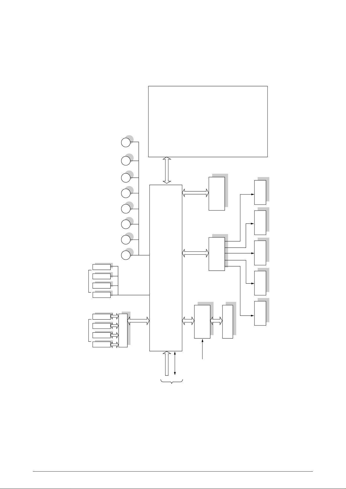
3. CIRCUIT DESCRIPTION
3.1 CU (controller unit : PCR)
3.1.1 Outline
The PCR PCB controls the reception of data transferred through a host I/F and processes
command analysis, bit image development, raster buffer read. It also controls the operator panel.
The block diagram of the entire OKIPAGE 8c including PCR PCB and details of PCR PCB are
shown in Figure. 3-1 and 3-2.
(1) Reception control
The OKIPAGE 8c has one centronics parallel I/F.
The centronics parallel I/F port can specify the following item when set by the control panel:
PARALLEL SPEED: HIGH/MEDIUM
BI-DIRECTION : ENABLE/DISABLE
I-PRIME : OFF/ON
An interface task stores all data received from the host into a receive buffer first.
(2) Command analysis processing
The OKIPAGE 8c has the following emulation mode.
Color Laser Jet : Hewlett Packard
PostScript Level 3 : Adobe
An edit task fetches data from the receive buffer, analizes commands, and reconstructs the
data in such a way that print data are aligned from up to down and from right to left; then it writes
the resultant data into a page buffer with such control data as print position coordinate, font
type, etc. added.
(3) Font Processing
When one page editing is finished, a developing task makes an engine start and fetches data
from the page buffer synchronizing with a printing operation; then it developes the fetched data
to a bit map as referring to data from a character generator, and writes the resultant data into
the raster buffer (of band buffer structure).
(4) Raster buffer read.
As controlling the engine operation, an engine task sends data from the raster buffer to the
LED head.
40985501TH Rev.1 4 /
Page 5

AC-IN AC switch
Crimp-style terminal
PXL board
PXL
Ejection sensor
LED head: Y M C K
Discharging lamp: Y M C K
Heat roller
thermistor
Backup roller
thermistor
Heater unit
SUMi card x 4
PD6 board
Y600 14P
YPOW 12P
M600 14P
MPOW 12P
C600 14P
CPOW 12P
K600 14P
KPOW 12P
HEAD1 13P HEAD2 14P HEADPOW 12P HEAD3 15P
FF form
sensor
Toner sensor x 4
ID sensor x 4
Low-voltage power supply
6P
6P'
JST3P
FAN 1
FAN 2
3P
Oil PAD MSW
FF
motor
Paper supply sensor board
FF Pos MSW
PXM board
40095001YU
REG.POS
sensor
Resist
motor
Y-IDU
motor
M-IDU
motor
C-IDU
motor
K-IDU
motor
Belt
motor
Heat
motor
PXF board
JODEN 8P
FSENS 8P
TONER
14P
PXFIF 30P
OPTION 7P
PENDTNR 6P
PX4 board
2nd tray
(option)
Form end
sensor
Waste toner
sensor
YIDREG
8P
MCKID
12P
HETBELT
8P
HEAD3
15P
HEAD2
14P
HEAD1
13P
HEADPOW
12P
FF 12P
PXFIF 30P
HVOLT 16P COVOPN 2P PSIZE 6P
High-voltage power supply
PXC board
Form size detector
Cover open
MSW
PCR
Operator
panel
PCO
board
CM
6P
PU 40P
72PX2
PS SIMM
72PX2
D-RAM SIMM
64P
OKI HSP
36P
Paralle
CUIF 40P
POWER 30P
THE.RM 6P
RSENS 7P
Interlock switch
UPDOWN
12P
40985501TH Rev.1 5 /
Figure 3-1 Block Diagram
Page 6

MPU Memory controller ROM, PS SIMM
SysAD
SysCmd
Control
64
9
5
SysAD
SysCmd
Control
A
D
Control
22
64
11
16244
16245
NMI
INTO
NR4700
LMQ-100
ExtReg
INT1
INT2
Reset
ColdReset
VCCOK
ModeIn
ModeClock
MasterClock
(Not installed)
External Agent
SysAD
SysCmd
Control
INT
REQ
ACK
AUX
CLK
RST
1
1
1
1
64
9
5
1
1
1
1
1
1
1
1
2
1
uPD94704
NMI
S1-001-F6
INT
CLK
RST
Interface controller
SysAD
SysCmd
Control
ExtReq
INT
ColdReset
VCCOK
ModeIn
ModeClk
uPU66044
GN-014-LMU
BusReq
BusAck
AUX
Reset
A
D
Control
WDATA
FSYNC
Control
PU I/F
OP I/F
EEPD
EEPCLK
EEPCS0
EEPCS1
PD
PCO
PCI
D
A
C
11
64
25
8
4
4
9
4
1
1
1
1
8
7
4
16
18
12
16244
D-RAM Max 80M
16245
16244
Engine
WDATA
ESYNC
Control
244
Operator
panel
244
EE-PROM #1
DI
CLK DO
CS
EE-PROM #2
DI
CLK DO
CS
74ACT1284 Bi-Centro
74ALS244
OKI HSP
Host I/F(Not installed)
PS -SIMM
OSC
Reset circuit
DIP SW
1
CLK
1
RSTIN
2
M
10
(TE6135 (6137), 16550, 53C80)
Figure 3-2 Block Diagram
40985501TH Rev.1 6 /
Page 7

3.1.2 CPU and Memory
(1) CPU (NR4700LMQ-100) (MIPS R4700)
CPU core : RISC CPU (MIPS R3000 compatible)
CPU clock : 100 MHz
Data bus clock : 50 MHz
Data bus width: Exterior 64 bits, Interior 64 bits
(2) ROM (HP Color LaserJet emulation)
ROM capacity : 8 Mbytes (16-Mbit mask or OTP ROM four pieces)
ROM type : 16 Mbits (1M x 16 bits)
Access time : 100 ns
(3) PostScript SIMM (Adobe PostScript emulation)
ROM capacity : 8 Mbytes [(16 Mbit ROM two pieces)x 2SIMMs]
ROM type : 16 Mbits (1M x 16 bits)
Access time : 100 ns
(4) Resident RAM
RAM capacity : 16 Mbytes (16 Mbit D-RAM eight pieces)
RAM type : 16 Mbits (1 M x 16 bits)
Access time : 60 ns
(5) Option RAM (SIMM: two slots)
RAM capacity : Max. 32 Mbytes (4 Mbytes, 8 Mbytes, 16 Mbytes, 32 Mbytes)
Access time : 60 ns, 70 ns, 80 ns
Note that only the product for ODA has been mounted with 16 Mbytes (8 Mbytes x 2) SIMM
as a resident.
The block diagram of CPU and memory circuits is shown in Figure 3-3.
40985501TH Rev.1 7 /
Page 8

DRAM01~04
(RAS0, CAS7~0)
Resident RAM
(16M Bytes)
Option SIMM
(Resident SIMM:
Only ODA)
Mask ROM
(8M Bytes)
Flash ROM
(2M Bytes)
PS SIMM
(8M Bytes)
DRAM11~14
(RAS2, CAS7~0)
SIMM0 H, L
(RAS4, 5, CAS7~0)
CAS01~04
(CS0)
PSIMMH, L
(CS2)
IFL1~4
(CS3)
(NR4700 LMQ-100)
CPU
(Memory Control LSI)
IMEM
(I/F Control LSI)
IIF
Control signals
AD [63 : 0]
CMD [7 : 0]
11
64
64
11
16244
16244
16244
16244
16245 x 4
16245 x 4
16Mbit DRAM x 4
16MbitMask ROM x 4
16MbitMask ROM x 2 x 2
4Mbit Flash ROM x 4
16Mbit DRAM x 4
Figure 3-3 Block Diagram of CPU & Memory
40985501TH Rev.1 8 /
Page 9

3.1.3 Reset Control
When power is turned on, a RESET-N signal is generated by the reset control IC (7705) which
checks +5V power supply.
OKI HSP
IMEM
µ
PD94704)
(
21
RT1
1
2
CT1
+5V
R620
22
25V
µ
1.5
4.7K
12
+5V
16V
CP13
C583
µ
21
21
47
Power ON
25V
µ
0.1
7
2
3
8
4
SEN
IN
CT
V+
GND
IRST1
7705
WRST
0V
RST
VREF
6
5
1
+5V
R590
12
25V
C586
µ
12
0.1
(
µ
PD66044)
4.7K
C50
12
100p 50V
IIF
HWRESET-N
Power OFF
RESET-N
COLDRST-N
Flash ROMs
CPU
(NR4700)
+5V
HWRESET-N
COLDRST-N
RESET-N
+3V
40985501TH Rev.1 9 /
Page 10

3.1.4 EEPROM Control
The NM93C46LN is an electrical erasable/programmable ROM of 64-bit x 16-bit configuration and
the NM93C66N is an electrical erasable/programmable ROM of 256-bit x 16-bit configuration.
Data input to and output from the ROM are bidirectionally transferred in units of 16 bits through
a serial I/O port (EEPDAT-P) in serial transmission synchronized with a clock signal from the I/F
control LSI(IIF).
IIF
(
µ
PD66044)
EEPDAT-P
154
EEPCS0-P
150
EEPCS1-P
165
EEPCLK-P
151
NM93C46LN
3
DI DO
1
CS
2
NM93C66N
3
DI DO
1
CS
2
SK
SK
4
E2ROM1
(PCR-PCB)
4
PSIMMH
(PS SIMM)
The EEPROM operates in the following instruction modes
Instruction Start Bit
Operation
Code
NM93C46LN
Address
NM93C66N
: Option
Data
Read (READ)
Write Enabled (WEN)
Write (WRITE)
Write All Address (WRAL)
Write Disabled (WDS)
Erase
Chip Erasable (ERAL)
1
1
1
1
1
1
1
10
00
01
00
00
11
00
A5 to A0
11XXXX 11XXXXXX
A5 to A0 A7 to A0
01XXXX 01XXXXXX
00XXXX 00XXXXXX
A5 to A0 A7 to A0
10XXXX 10XXXXXX
A7 to A0
D15 to D0
D15 to D0
40985501TH Rev.1 10 /
Page 11
CS
SK
CS
SK
DI
DO
Write cycle timing (WRITE)
101
HIGH-Z
A5/A7
Read cycle timing (READ)
A4/A6
A1 A0 D15
D14
Min. 450 ns
STATUS
D1 D0
Max. 500 ns
BUSY READY
Max. 10 ms
DI
DO
HIGH-Z
11 0
A5/A7 A4/A6
A1 A0
A5/A7
A4/A6
D1 D00
40985501TH Rev.1 11 /
Page 12
3.1.5 Centronics Parallel Interface
The CPU sets a BUSY-P signal to ON at the same time when it reads the parallel data
(CENTDATA1-P to CENTDATA8-P) from the parallel port at the fall of STB-N signal. Furthermore,
it makes the store processing of received data into a receive buffer terminate within a certain fixed
time and outputs an ACK-N signal, setting the BUSY-P signal to OFF.
IIF
(
µ
PD66044)
87, 88, 91 to 96
97
85
86
83
81
79
80
82
84
PDATA [7 : 0]
STB-N
BSY-P
ACK-N
PE
SEL
FAULT
INIT-N
SELIN-N
AUTOFEED
IC16, 17
IC17
IC17
IC17
IC16
IC16
2 to 9
11
10
12
13
32
31
36
+5V 14
18
FU2
1A
CENT
DATA8-P
DATA1-P
STB-N
1
BUSY-P
ACK-N
PE-P
SEL-P
FAULT-N
IPRIME-N
SELIN-N
AUTOFEED-N
+5V
to
PARALLEL DATA
(DATA BITs 1 to 8)
0.5 µs min.
0.5 µs min.
0.5 µs min.
nStrobe
0.5 µs min.
0.5 µs max.
Busy
0 min.
0 min.
nAck
0.5 µs to 10 µs
0 min.
40985501TH Rev.1 12 /
Page 13

3.1.6 Operator Panel Control
The operator panel consists of the following circuits.
PCR- PCO-
IIF
(µPD66044)
I/F Control LSI
OPCMD-P
146
OPSTS-P
147
OPSCLK-P
149
OPLOAD-N
150
IC19
3
4
6
1
CN1PANEL
4
3
1
6
Flexible
Cable
(1) BU6152S (LSI)
This LSI is connected to a clock synchronous serial port of the I/F Control LSI (IIF). It controls
switch data input, LED data output and LCD data input/output according to the commands
given by the I/F Control LSI. The I/F Control LSI sends the 2-byte (16-bit) command (OPCMDP) together with the shift clock signal (OPSCLK-N) to the Operator Panel Control LSI and then
makes a predetermined input/output control if the command decoded by the Operator Panel
Control LSI is found to be a normal command.
BU6152S
Operator Panel
Control LSI
DB4~DB7
RS
R/W
E
LED
44780
LCD
Control
Driver
Zebra Rubber
LCD
On receiving a command sent from the I/F Control LSI, the Operator Panel Control LSI,
synchronizing with the serial clock of the command, returns a 2-byte command response to
the I/F Control LSI.
OPCMD-P
OPSCLK-N
OPSTS-P
OPLOAD-N
bit 0 bit 15
Command
bit 0
bit 15
Command response
40985501TH Rev.1 13 /
Page 14

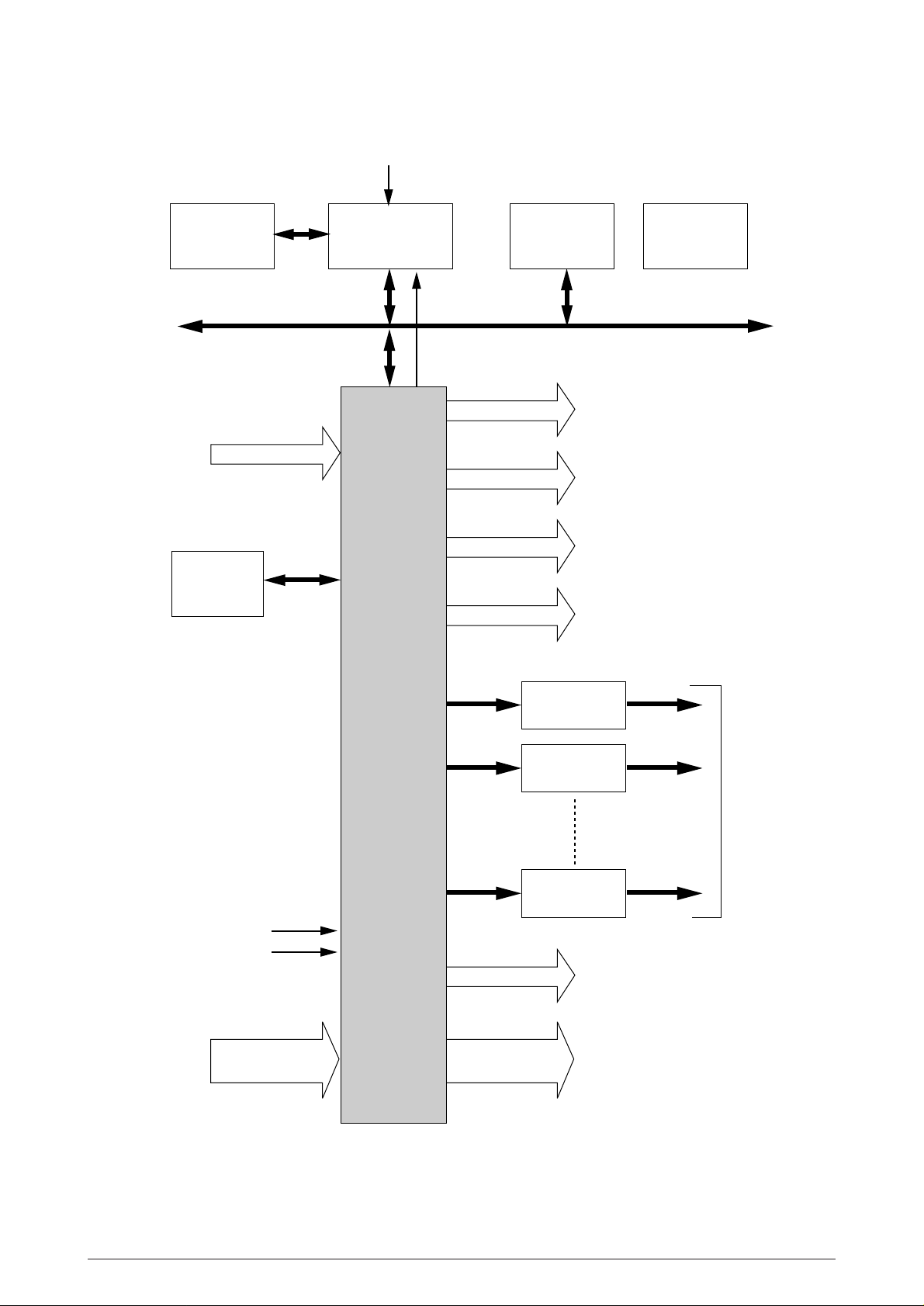
3.2 PU (Printer Unit : PX4)
3.2.1 Outline
PU section executes controls such as LED head control, stepping motor control, high-voltage
control, video I/F control, command I/F control and fusing control, and performs color image
printing. The block diagram is shown in Fig3-4.
(1) The print data stored in the video memory is loaded to the LED head control and transferred
through each line to the LED head to light LEDs. This causes a static latent image to form on
the photoconductive drum I.
(2) Stepping motor control: executes ID up/down control for the supply, carriage and ejection of
print media
(3) High-voltage power supply control: executes ON/OFF control for various kinds of power supply
units through serial interface.
(4) Fusing control: executes the control of fusing temperature according to the type of media.
(5) Video I/F control: receives the print data from the controller section (CU) and stores it to the
video memory.
(6) Command I/F control: executes the receiving control of commands from the controller section
(CU) and sending control of status signals.
40985501TH Rev.1 14 /
Page 15
PD6-PCB
Low Voltage
Power Supply
High Voltage
Power Supply
Belt Unit
Y-ID Unit
M-ID Unit
C-ID Unit B-ID Unit
Second Tray
(option)
Fuser Unit
LED Head Eraser Lamp
M
M M M
M M
M M
Y-ID M-ID C-ID B-ID BELT HEATER REGIST FRONT
Stepping Motor
PX4-PCB
PXF-PCB
VIDEO I/F
COMMAND I/F
AC 120V/230V
<Sensors>
• Outlet sensor
• Inlet sensor1
• Inlet sensor2
• Write sensor
• Paper width sensor
• Humidity sensor
• Temperature sensor
• Paper end sensor
• Toner sensors (Y.M.C.K)
• ID Up/Down sensors (Y.M.C.K)
• Waste toner full sensor
• Waste box sensor
• Paper size sensor
• Oil roller sensor
• FF home sensor
• FF Paper end sensor
• Pinch roller up/down sensor
From CU
40985501TH Rev.1 15 /
Figure 3-4 Block Diagram
Page 16

3.2.2 CPU, Memory and LSI
(1) CPU (MSM65524)
CPU core : nX8 (Oki original)
CPU clock : 10 MHz
Data bus clock : 50 MHz
Data bus width: 8 bits
(2) ROM (27512)
ROM capacity : 64K bytes
ROM type : 512K bits, 8 bits
Access time : 150 ns
(3) Resident RAM (62256)
RAM capacity : 32K bytes (Static RAM)
Access time : 70 ns
(4) VIDEO RAM (658512)
RAM capacity : 512K bytes (Pseudo Static RAM)
Access time : 70 ns
The block diagram of CPU, memory and LSI circuits is shown in Figure 3-5.
40985501TH Rev.1 16 /
Page 17
Analogy input (Temperature, Humidity, etc)
CPU BUS
VIDEO I/F
EEPROM
NM93C66N
VIDEO MEM
HM658512
CPU
MSM65524
(include AD Converter)
ROM
27512
Y HEAD I/F (3.3V)
M HEAD I/F (3.3V)
C HEAD I/F (3.3V)
B HEAD I/F (3.3V)
RAM
62296
MT DRIVER
MTD2005F
MT DRIVER
MTD2005F
LSI
(MB87D113)
MT DRIVER
MTD2005F
RESET
CLOCK
High voltage Power Supply Serial I/F (2CH)
Input Port Output Port
Stepping Motor x 8
Figure 3-5 Block Diagram of CPU, Memory & LSI
40985501TH Rev.1 17 /
Page 18

3.2.3 Reset Control
When power is turned on, a RST-N signal is generated by the rising sequence of +5V power supply.
+5V
µ
21
C21
25V 0.1
0VL
PST592
VCC
GND
IC3
OUT
1
R61
0.1W 3.3K
2
13
IC12
QC
LS07
+5V
R63
0.1W 1K
21
Ω
22K
12
2
1
Q11
+5VD
3
Q12
2
D2
23
3
1
IC12
12
QC
+5V
0.1W 3.3K
R60
21
RST-N
+5V
RST-N
+5VD
LS07
Power OFF
Power ON
4V
Approx. 110ms Approx. 20ms
40985501TH Rev.1 18 /
Page 19

3.2.4 EEPROM Control
The NM93C66N is an electrical erasable/programmable ROM of 256-bit x 16-bit configuration.
Data input to and output from the ROM are bidirectionally transferred in units of 16 bits through
a serial I/O port (out DATA-P and IN DATA-P) in serial transmission synchronized with a clock
signal from the CPU(IC10).
IC10
(MSM65524)
OUT DATA-P
15
EEPRMCS0-P
13
INDATA-P
16
EEPRMCLK-P
14
NM93C66N
3
DI DO
1
CS
The EEPROM operates in the following instruction modes
Instruction Start Bit
Read (READ)
Write Enabled (WEN)
Write (WRITE)
Write All Address (WRAL)
Write Disabled (WDS)
Operation
Code
1
1
1
1
1
10
00
01
00
00
Address
NM93C66N
11XXXXXX
01XXXXXX
00XXXXXX
SK
2
A7 to A0
A7 to A0
4
IC2
(PX4-PCB)
Data
D15 to D0
D15 to D0
Erase
Chip Erasable (ERAL)
1
1
11
00
A7 to A0
10XXXXXX
40985501TH Rev.1 19 /
Page 20

CS
SK
CS
SK
DI
DO
Write cycle timing (WRITE)
101
HIGH-Z
A7
Read cycle timing (READ)
A6
A1 A0 D15
D14
Min. 450 ns
STATUS
D1 D0
Max. 500 ns
BUSY READY
Max. 10 ms
DI
DO
HIGH-Z
11 0
A7 A6
A1 A0
D1D14D15 D00
40985501TH Rev.1 20 /
Page 21

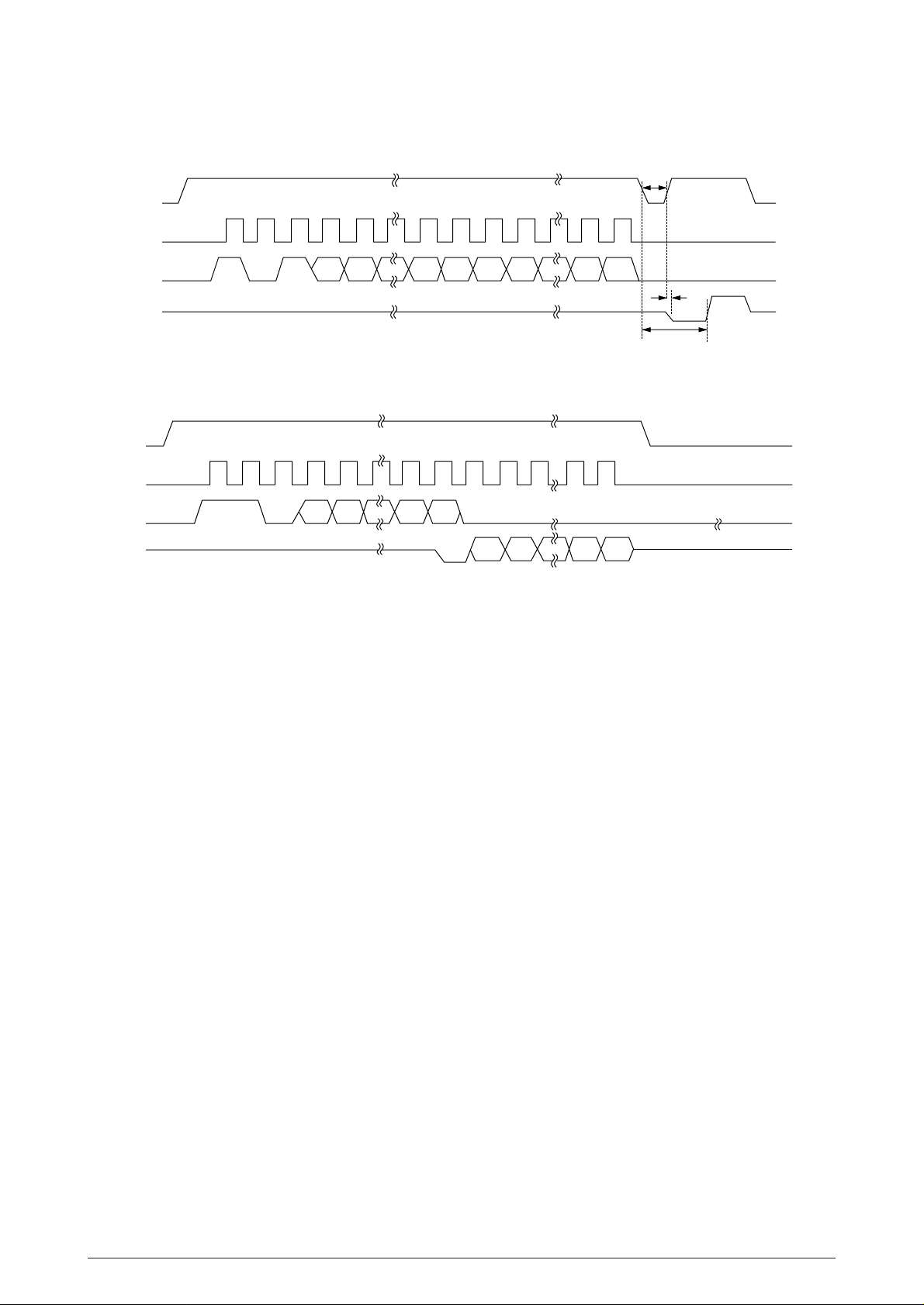
3.2.5 LED Head Control
LSI PIN
LSI
IC1
(MB87D113)
PX4-PCB
Y
M
C
K
Signal
HDDTY3
HDDTY2
HDDTY1
HDDTY0
STBY3
STBY2
STBY1
STBY0
HDCK0
HDLD0
HDDTM3
HDDTM2
HDDTM1
HDDTM0
STBM3
STBM2
STBM1
STBM0
HDCK1
HDLD1
HDDTC3
HDDTC2
HDDTC1
HDDTC0
STBC3
STBC2
STBC1
STBC0
HDCK2
HDLD2
HDDTK3
HDDTK2
HDDTK1
HDDTK0
STBK3
STBK2
STBK1
STBK0
HDCK3
HDLD3
Lsi Pin
IC1-136
IC1-135
IC1-134
IC1-133
IC1-144
IC1-143
IC1-142
IC1-141
IC1-137
IC1-140
IC1-149
IC1-148
IC1-147
IC1-146
IC1-157
IC1-155
IC1-154
IC1-153
IC1-151
IC1-152
IC1-161
IC1-160
IC1-159
IC1-158
IC1-169
IC1-168
IC1-167
IC1-166
IC1-164
IC1-165
IC1-173
IC1-172
IC1-171
IC1-170
IC1-181
IC1-180
IC1-179
IC1-178
IC1-176
IC1-177
CN2CN1 CN3 HEAD CN
PD6-PCB
CN1
HEAD1-4
HEAD1-3
HEAD1-2
HEAD1-1
HEAD1-10
HEAD1-9
HEAD1-8
HEAD1-7
HEAD1-5
HEAD1-6
HEAD2-1
HEAD1-13
HEAD1-12
HEAD1-11
HEAD2-7
HEAD2-6
HEAD2-5
HEAD2-4
HEAD2-2
HEAD2-3
HEAD2-11
HEAD2-10
HEAD2-9
HEAD2-8
HEAD3-3
HEAD3-2
HEAD3-1
HEAD2-14
HEAD2-12
HEAD2-13
HEAD3-9
HEAD3-8
HEAD3-7
HEAD3-6
HEAD3-15
HEAD3-14
HEAD3-13
HEAD3-12
HEAD3-10
HEAD3-11
CN2
HEAD1-4
HEAD1-3
HEAD1-2
HEAD1-1
HEAD1-10
HEAD1-9
HEAD1-8
HEAD1-7
HEAD1-5
HEAD1-6
HEAD2-1
HEAD1-13
HEAD1-12
HEAD1-11
HEAD2-7
HEAD2-6
HEAD2-5
HEAD2-4
HEAD2-2
HEAD2-3
HEAD2-11
HEAD2-10
HEAD2-9
HEAD2-8
HEAD3-3
HEAD3-2
HEAD3-1
HEAD2-14
HEAD2-12
HEAD2-13
HEAD3-9
HEAD3-8
HEAD3-7
HEAD3-6
HEAD3-15
HEAD3-14
HEAD3-13
HEAD3-12
HEAD3-10
HEAD3-11
Y HEAD
M HEAD
C HEAD
K HEAD
CN3
Y600-5
Y600-4
Y600-8
Y600-7
Y600-14
Y600-13
Y600-12
Y600-11
Y600-2
Y600-10
M600-5
M600-4
M600-8
M600-7
M600-14
M600-13
M600-12
M600-11
M600-2
M600-10
C600-5
C600-4
C600-8
C600-7
C600-14
C600-13
C600-12
C600-11
C600-2
C600-10
K600-5
K600-4
K600-8
K600-7
K600-14
K600-13
K600-12
K600-11
K600-2
K600-10
HEAD CN
Y-5
Y-4
Y-8
Y-7
Y-14
Y-13
Y-12
Y-11
Y-2
Y-10
M-5
M-4
M-8
M-7
M-14
M-13
M-12
M-11
M-2
M-10
C-5
C-4
C-8
C-7
C-14
C-13
C-12
C-11
C-2
C-10
K-5
K-4
K-8
K-7
K-14
K-13
K-12
K-11
K-2
K-10
40985501TH Rev.1 21 /
Page 22

PX4-PCB
LED Head
IC1
(MB87D113)
HDDTX0
HDDTX1
HDDTX2
HDDTX3
HDCLKX
HDLDX
STBX0
STBX1
STBX2
STBX3
5
4
8
7
2
10
14
13
12
11
Head Lsi
with EEPROM
Driver IC
Driver IC Driver IC
Driver IC
38
X=Y, M, C or B
Data is transferred to the head unit starting with the data at the left end of the paper in the
synchronous serial transfer mode using the HDCKX signal as the sync signal.
The total number of LEDs in the head unit is 4992. The data for the driver latches causes the
corresponding LEDs to light only during the time when the STBXn signal is output. There are four
STBXn signals (STBX0, STBX1, STBX2 and STBX3), each of which controls the corresponding
driver for 1248 LEDs (4992/4).
The four STBXn signals must be output within the time when the LEDs for one line continue to emit
light. After the data is moved to the latches by the STBXn signal, the transfer of the data of the next
line can be started.
40985501TH Rev.1 22 /
Page 23

The timing chart for the outline of this operation is shown below.
HDCKX
HDDTX0
HDDTX1
HDDTX2
1
59
2 6 10 4986 4990
3
11 4987 4991
7
4985
4989
✰
The LED lights
when the head
data is HIGH.
HDDTX3
HDCKX
HDDTX0
HDDTX1
HDDTX2
HDDTX3
HDLDX
STBX0
STBX1
STBX2
STBX3
4 8 12 4988 4992
Each figure denotes the dot
position taking the left end bit
position as "1".
Print activation
timing for the
1st line
LEDs
1-1248
lit
LEDs
1249-2496
lit
LEDs
2497-3744
lit
Print activation timing
for the 2nd line
LEDs
3745-4992
lit
Print activation timing
for the final line
40985501TH Rev.1 23 /
Page 24

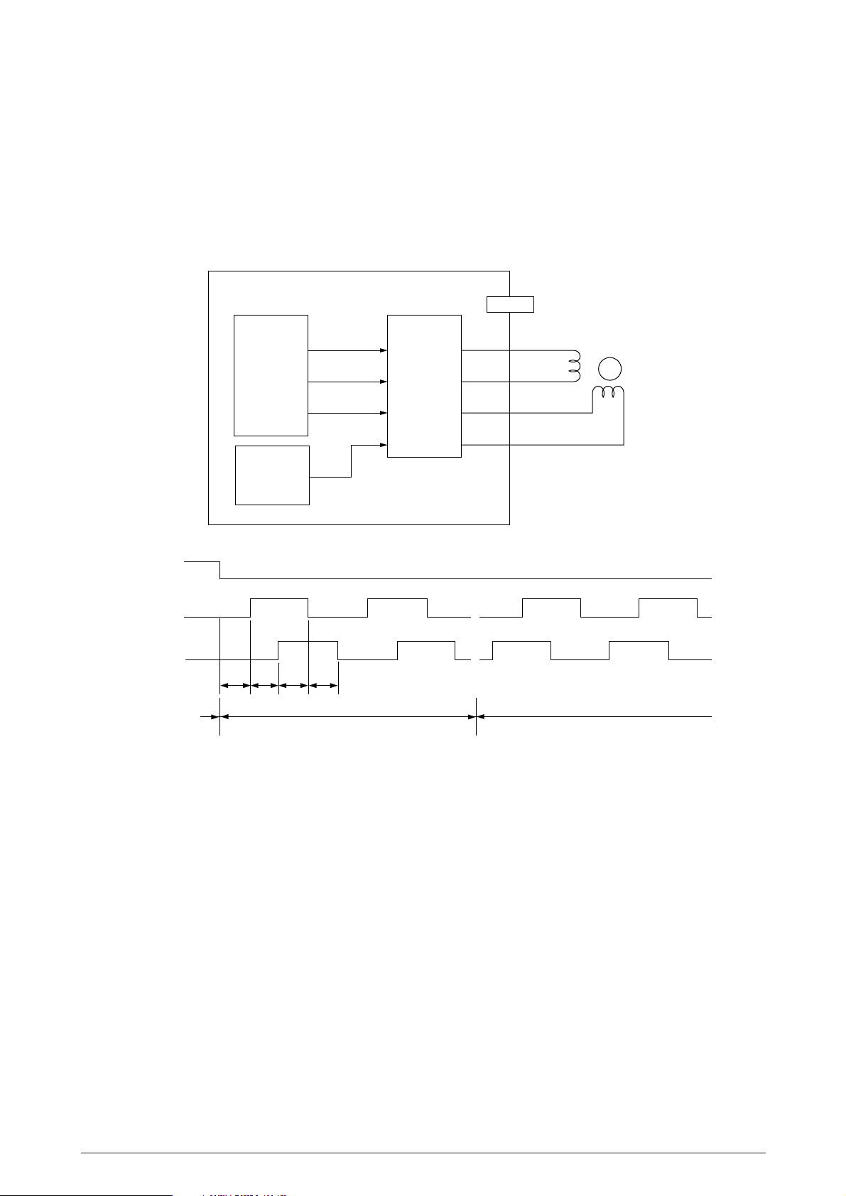
3.2.6 Motor Control
OKIPAGE 8c controls the paper flow by eight motors (Four ID Motors, Hopping Motor, Front feed
Motor, Belt Motor).
(1) ID motor
The four ID motors for rotate four color IDs are driven by the driver IC according to the control
signal from the IC1 (MB87D113).
The IC8 (62354) is a Digital to Analogy Converter controlled by CPU (IC10 : MSM65524) and
its output voltage controls several ID motor current.
40985501TH Rev.1 24 /
Page 25

IC1 (MB87D113)
189
188
111
YIDON
190
192
191
MIDON
193
195
194
CIDON
196
200
199
KIDON
201
YIDPHA
YIDPHB
IDMOTON-N
MIDPHA
MIDPHB
CIDPHA
CIDPHB
KIDPHA
KIDPHB
26
17
27
16
23
20
26
17
27
16
23
20
26
17
27
16
23
20
26
17
27
16
23
20
IC15
MTD2005F
IC16
MTD2005F
IC17
MTD2005F
IC18
MTD2005F
Y-ID REG
3
7
8
12
3
7
8
12
3
7
8
12
3
7
8
12
1
3
2
4
9
11
10
12
5
7
6
8
1
3
2
4
Y-ID motor
M
M-ID motor
M
C-ID motor
M
K-ID motor
M
IDREF
IDMOTON-N
XIDON
XIDPHA
XIDPHB
Rotation
IC8
(62354)
Power ON
6
IDREF
Initial process
Stop
T0 T1 T2
T3
T4 T5 T6
Reverse rotation
Forward rotation speed : T0 to T3= (Print operation)
Reverse rotation speed : T4 to T7= (ID up operation)
T7
40985501TH Rev.1 25 /
Page 26

(2) Regist motor
The Regist motor is driven by the driver IC14 according to the control signal from the LSI (IC1:
MB87D113). The Regist motor current is controlled by the DAC (IC8 : 62354).
REGON
REGPHA
REGPHB
PX4-PCB
IC1
(MB87D113)
IC8
(62354)
T0 T1 T2 T3
REGPHA
203
REGPHB
202
REGON
204
REGREF
11
26
17
27, 16
23, 20
IC14
(MTD2005F)
3
7
8
12
YIDREG
5
7
6
8
T4 T5 T6 T7
Regist
Motor
M
Rotation
Stop
Forward rotation
Reverse rotation
(Hopping operation) (Regist operation)
Hopping Operation speed: T0 to T3 =
Regist Operation speed: T4 to T7 =
µ
s
µ
s
40985501TH Rev.1 26 /
Page 27

(3) Front feed motor
The Front feed motor is driven by the driver IC13 according to the controll signal from the LSI
(IC1 : MB87D113).
The Regist motor current is controlled by the DAC (IC8 : 62354)
FFON
FFPHA
FFPHB
PX4-PCB
IC1
(MB87D113)
IC8
(62354)
T0 T1 T2 T3
211
208
212
12
FFPHA
FFPHB
FFON
FFREF
26
17
27, 16
23, 20
IC13
(MTD2005F)
FF
Front Feed
3
Motor
M
7
8
12
T4 T5 T6 T7
Rotation
Stop
Forward rotation
Reverse rotation
(Paper feed operation) (Pinch roller up/down operation)
Paper feed operation speed: T0 to T3 =
Pinch roller up/down operation speed: T4 to T7 =
µ
s
µ
s
40985501TH Rev.1 27 /
Page 28
(4) Belt motor
The Belt motor is driven by the driver IC19 according to the control signal from the LSI (IC1
: MB87D113).
The Belt motor current is controlled by the DAC (IC8 : 62354).
BELTON
BELTPHA
BELTPHB
PX4-PCB
IC1
(MB87D113)
IC8
(62354)
T0 T1 T2 T3
BELTPHA
21
BELTPHB
20
BELTON
22
BELTREF
9
26
17
27, 16
23, 20
IC19
(MTD2005F)
3
7
8
12
HETBELT
5
7
6
8
Belt Motor
M
Rotation
Forward rotation
(Belt feed operation)
Belt feed speed: T0 to T3 = µs
Reverse rotationStop
40985501TH Rev.1 28 /
Page 29

(5) Heat motor
The Heat motor is driven by the driver IC20 according to the control signal from the LSI (IC1
: MB87D113).
The Heat motor is controlled by the DAC (IC8 : 62354).
HETON
HETPHA
HETPHB
PX4-PCB
IC1
(MB87D113)
IC8
(62354)
T0 T1 T2 T3
HEATPHA
206
HEATPHB
205
HEATON
207
HEATREF
10
26
17
27, 16
23, 20
IC20
(MTD2005F)
3
7
8
12
HETBELT
1
3
2
4
Heat Motor
M
T4 T5 T6 T7
Rotation
Stop
Forward rotation
(Heating operation)
Heating speed: T0 to T3 = µs
Reverse rotation
40985501TH Rev.1 29 /
Page 30
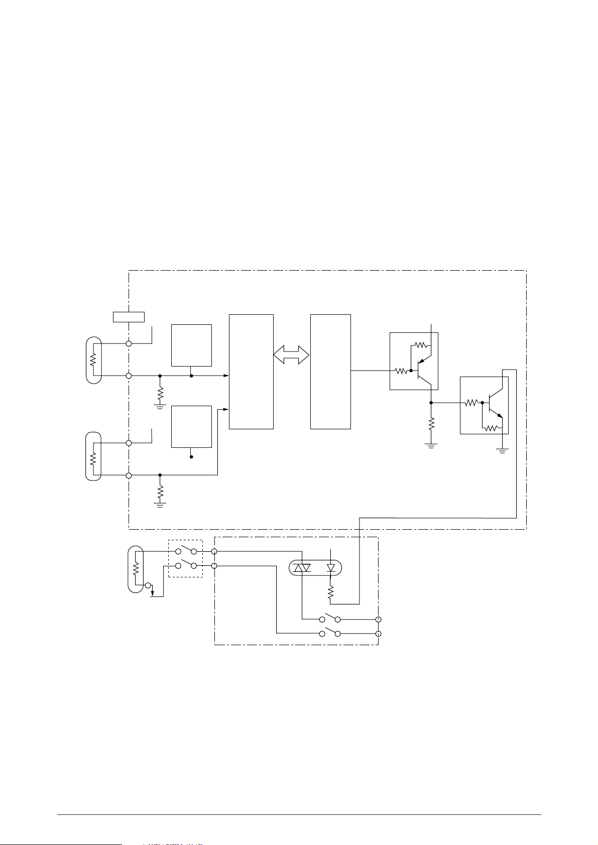
3.2.7 Fuser Temperature Control
For the temperature control by heater control, the variation in the resistance of the thermistor is A/
D converted in and the resultant digital value is read and transferred to the CPU. The CPU turns
on or off the HEATON-N signal according the value of the signal received from to keep the
temperature constant.
Immediately after the power is turned on, the thermistor is checked for shortcircuit and breakdown.
If the thermistor is shorted, the A/D converted value shows an extremely high temperature, so that
the shortcircuit can be detected. If the breakdown of the thermistor occurs, the A/D converted value
shows the normal temperature. In this case, the thermistor breakdown can be detected by the
sequence shown at the end of this section. If the heater is overheated, 5V supply is turned off by
detecting that the resistance of the thermistor exceeds the predetermined value.
PX4-PCB
Heat roller
Thermistor
: TH
Back-up roller
thermistor
: TB
Thermostat
Heater
THERM
+5V
+5V
Interlock SW
Thermistor
Thermistor
breakdown
detect
circuit
Thermistor
breakdown
detect
circuit
IC10
(MSM65524)
AD7
60
AD6
59
5V
Low Voltage Power Supply
Bus
IC1
(MB87D113)
+5V
HEATON-N
237
Q13
+5VD
Q10
AC120V/230V
Power SW
40985501TH Rev.1 30 /
Page 31

The temperature control is described below.
T : Heat roller temperature
Temperature
˚C
T
P
T = 150˚C
H
T= + 1/2
T
T
H
B
C Hopping C Hopping
H
T : Back-up roller temperature
B
T : Printing temperature
P
ON OFF OFFHEATON-N
Heater is controlled by CPU (IC10 : MSM65524) as followings.
Temperature
T<150˚C
150˚C<T<T
T <T
P
Relationship of the printing temperature (T ) and speed against media type as follows.
Media type
Light
Medium Light
Medium
Medium Heavy
Heavy
Special
Transparency
P
HEATON-N
ON
C Hopping
OFF
T
P
200˚C
200˚C
215˚C
215˚C
220˚C
225˚C
220˚C
P
Print Speed
8ppm
8ppm
8ppm
8ppm
8ppm
6ppm
6ppm
40985501TH Rev.1 31 /
Page 32

To detect the breakdown of the heater, the heater is turned on. If the corresponding temperature
rise is not detected, it is judged that heater breakdown occurs. To shorten the breakdown detecting
time, the following circuit is used. When the thermistor is checked for breakdown immediately after
the power is turned on, the THCHK-N signal is turned on to turn transistors Q1 and Q506 off. As
a result, the thermistor serial resistance is varied to increase the reading resolution.
5V
IC10
Heat roller
Thermistor
5V
Q1
(MSM65524)
Back-up roller
Thermistor
5V
IC1
(MB87D113)
230
Q506
40985501TH Rev.1 32 /
Page 33

3.2.8 Fan Motor Control
OKIPAGE 8c has two cooling fans.
The stop/rotation of the fan motor is controlled by a FANON0-P and FANON1-P signals. When
the fan motor rotates normally, a FANERR0-P and FANERR1-P signals generated in the hole
element built in the fan motor is input to the IC1 (MB87D113).
PX4-PCB
IC1
(MB87D113)
+32V
FAN1
FANON0-P
233
FANERR0-P
239
FANON1-P
232
FANERR1-P
238
FAN Motor1
1
+5V
M
2
3
+32V
POWER
FAN Motor2
19
+5V
M
20
Low Voltage Power Supply
n
FANON -P
FANALARM -N
n
1 sec max
0.7 sec max
FAN MOVE
Lockn=0, 1
Fan motor start:Power on
Fan motor stop: • The motor immediately stops when a fan error occurs.
• The motor stops in the cover open state (fan1 only).
40985501TH Rev.1 33 /
Page 34

3.2.9 Sensor Supervision
OKIPAGE8c unit is provided with 23 sensors.
The sensor signals are read directly from the input ports of CPU (IC10: MSM65524) and LSI (IC1:
MB87D113).
Front Feeder Unit
Pinch roller
up/down sensor
Front feeder
paper end sensor
Front feeder
Home position sensor
PD6-PCB
PENDF-N
EFPOS-N
PX4-PCB
2
3
22
IC10
(MSM65524)
IC1
(MB87D113)
6
10
9
8
7
57
58
10
217, 218
219,220
213, 214
215, 216
15
HEATR-N
HOP-N
PAPIN-N
PAPW1D-N
PSWR-N
HUM-P
TEMP-P
PEND-N
TNRY.M.C.K
IDPOSY.M.C.K
TNRFUL-N
PXF-PCB
4
4
PXM-PCB
Inlet
sensor1
Inlet
sensor2
Write
sensor
Paper width
sensor
Humidity
sensor
Temperature
sensor
Paper end
sensor
Toner
sensor(Y.M.C.K)
ID up/down
sensor(Y.M.C.K)
Wast toner
full sensor
OILPAD
Oil roller
sensor
27
16
TNRBOX-N
4, 5, 8, 9 4
PAPSIZE0~3
Toner box
sensor
PXC-PCB
1st Tray
Paper size sensor board
40985501TH Rev.1 34 /
Page 35

3.2.10 Cover Open
When the cover (upper cover, side cover, front cover) is opened, a cover open microswitch opened.
This makes a CPUCVOPN signal low, then off the +5VD, thereby the CPU detects the open state.
Furthermore, opening the cover stops applying a +32V power to the high voltage power supply unit
and stepping motor drivers, and stops applying a AC120V/230V power to the fuser unit, resulting
in stopping all high voltage outputs, motor driver outputs and heater output.
High Voltage
Power Supply
High Voltage
output
Low Voltage
Power Supply
AC120V/
230V
+32V
HTDV HTDV HTDV
stepping motor drivers
5VD+5V
11
IC10
(MSM65524)
PX4-PCB
MSW x 3
(Upper cover, side cover and Front cover)
Fuser Unit
Interlock SW
(Upper cover)
CPUCVOPN
+5VD
0V
Cover close Cover open
40985501TH Rev.1 35 /
Heater
Page 36

3.2.11 Power Supply Interface
The power supply interface is a 16 bit clock synchronous serial interface between the synchronous
serial I/O ports of CPU (IC1: MB87D113) and the power control LSI in the power supply board (High
voltage) under the control of the CPU (IC10: MSM65524).
When the control section transmits a command on POWDOUTn-P signal in synchronization with
the clock (POWSCLKn-N) to the power supply board, this power supply board transmits a
response on POWDINn-N signal in synchronization with the same clock to the control section.
The commands include the control data of the high-voltage power supply, etc.
The responses include high voltage output value, etc.
PX4-PCB
(MB87D113)
IC10
(MSM65524)
IC1
225
224
226
HVOLT
POWDOUT1-P
POWSCLK1-N
POWDIN1-P
High Voltage Power Supply Board
LSI
POWDOUTn-P
POWSCLKn-N
POWDINn-P
POWSQCR-N
223
228
227
229
LSB
b0 b1 b2 b3 b4 b5 b6 b7 b8 b9 b10 b11 b12 b13 b14 b15
POWSQCR-N
POWDOUT2-P
POWSCLK2-N
POWDIN2-P
Command
MSB
Response
b0 b1 b2 b3 b4 b5 b6 b7 b8 b9 b10 b11 b12 b13 b14 b15
LSI
n=1, 2
40985501TH Rev.1 36 /
Page 37

3.2.12 Option (2nd paper feeder) Interface
The option interface is a 8 bit clock synchronous serial interface between the synchronous serial
I/O ports of CPU (IC10: MSM65524) and 4 bit micro-controllers in the option control boards under
the control of the CPU (IC10: MSM65524).
First the control section transmits a command on OPTSD-P signal in synchronization with the clock
(OPTSCLK-N) to the option.
The option which receives the command will analyze it and assert OPTSDR-N signal after
becoming a ready state for returning a response. When the control section recognizes the
OPTSDR signal asserted, it will output a clock signal only at this time.
The option will output a response on the OPTSD-P signal line in synchronization with this clock
signal (OPTSCLK-N).
The commands include the control data, etc.
The responses include sensor information, etc.
OPTSD-P
OPTSCLK-N
OPTSDR-N
Jackln connector
PX4-PCB PXF-PCB
PXFIF
IC10
(MSM65524)
b0 b1 b2 b3 b4 b5 b6 b7 b0 b1 b2 b3 b4 b5 b6 b7
OPTSD-P
OPTSCLK-N
OPTSDR-N
COMMAND RESPONSE
PXFIF OPTION
A4
A4
B3
B3
B4
B4
(14P)
3
2
4
Jackln connector
(14P)
AOLO-PCB (2nd paper feeder)
Control
circuit
40985501TH Rev.1 37 /
Page 38

3.2.13 Power Supply Board
The power supply circuit consists of the low-voltage power supply circuit and the high-voltage
power supply circuit. The low-voltage power supply circuit adopts a switching power supply system
and provides DC voltages required for the control of the equipment. The high-voltage power supply
circuit receives low-voltage power from the low-voltage power supply circuit and provides various
high voltages required for the electrophotographic process according to the control signals from
the control section.
(1) Low-voltage power supply circuit
SW
F1 F52
ACIN
Noise
filter
circuit
Switching
circuit/
Resonation
Rectifying/
smoothing
circuit
+8V
–8V
ACON-N
POW ON
Heater
control
circuit
ACOUT
(CN1)
Switching /
resonance
control
circuit
Rectifying/
smoothing
circuit
Rectifying/
smoothing
circuit
over voltage/
over current
detector
circuit
F51
regulating
circuit
Voltage
detector
circuit
+32V
+3.3V
over voltage/
over current
detector
+5V
+12V
-12V
+32V
+5V
+ 5V
+ 32V
+ 3.3V
+ 12V
– 12V
40985501TH Rev.1 38 /
Page 39

(2) High-voltage power supply circuit
This high-voltage power supply circuit receives the high-voltage generation timing control
command that is transmitted in serial through the power supply interface from the control
section. It decodes this command by LSI (IC102, 201) and outputs high-frequency pulses
(PWM) to the corresponding high-voltage generating circuits through pins 11, 12, 13, 14, 15,
16, 17 and 18 of LSI (IC102, 201). It supplies +38V to each high-voltage generating circuit
as the source voltage. When the cover is open, the supply of +32V is interrupted to interrupt
all the high-voltage outputs. The relationship between the PWM output pins and the highvoltage outputs is shown in the following table.
Power Supply Board (High voltage)
Control section
G/A
+5V
+32V
+5V
+32V
LSI
(IC102)
LSI
(IC201)
11
12
13
14
15
16
17
18
11
13
15
+5V
DB2(-)
(common)
+5V
DB1(+)
+5V/+12V
Reference
generation
+5V
+5V
+5V
TR-Y
DB2(-)
(common)
DB2(-)
(common)
DB2(-)
(common)
DB2(-)
(common)
SB1(+)
SB2(-)
FIX
CH
+32V
TR-Y
DB-Y
DB-M
DB-C
DB-B
SB
FIX
CH
TR-Y
+12V
40985501TH Rev.1 39 /
+12V
Reset
circuit
Output inhibit
circuit
LSI Reset
16
17
18
Reference
generation
Reference
generation
Reference
generation
TR-M
TR-C
TR-B
TR-M
TR-C
TR-B
TR-M
TR-C
TR-B
Page 40

[IC102]
PWM
output pins
High-voltage
outputs
DB-Y DB-M DB-B SB
DB-C
11
11, 12
11, 13
11, 14
11, 15
16
17
18
—
-275V
+300V
—
-275V
+300V
—
-275V
+300V
-290V
+300V
+450V
-450V
Note 1) No output for 11 only. When DB2(-) is outputted, pulse is outputted simultaneously.
Note 2) -255V only for the first page printing
[IC201]
High-voltage
PWM
output pins
outputs
11
FIX CH TR-M TR-C
TR-Y
0.5~2.5KV
TR-B
13
15
16
17
18
1.35KV
0.5~4KV
0.5~4KV
0.5~4KV
0.5~4KV
40985501TH Rev.1 40 /
Page 41

Interface command
A.Output ON/OFF
b13
DB1
0
Higher 8 bits
b120b11
DB2-Y, M, C, B
BCMY
b10
b9
0
0
SB2
0
CH
0
b8
DB2
common
DB1/SB1
common
FIX
CHAN1
CHAN2
Lower 8 bits
22
30H
10H
30H
b14
b15
SB1
SB2
0
0
TR-Y, M, C, B
BCMY
Note 1) With the bit corresponding to each output, if it is 0, OFF and 1, ON.
Note 2) The output which has plural bit control is outputted by AND condition (where
both bits are 1(ON)). Also, the combination of bits such as reverses output
polarity is prohibited.
B. Output voltage settings
CHAN1
Lower 8 bits
34H
44H
54H
64H
Pertinent
output
DB-Y
DB-M
DB-C
DB-B
Higher 8 bits
DB2 Output voltage setting value
74H
84H
94H
CHAN2
24H
44H
64H
74H
84H
94H
C. Output current measurement
Read command
(Lower 8 bits)
CHAN2
17H
DB1
SB1
SB2
FIX
CH
TR-Y
TR-M
TR-C
TR-B
DB1 Output voltage setting value
SB1 Output voltage setting value
SB2 Output voltage setting value
FIX Output voltage setting value
CH Output voltage setting value
TR Output voltage setting value
Read data
(Higher 8 bits reply)
Measured current value of FIX output
Note 1)
40985501TH Rev.1 41 /
Page 42

3.3 PCR-PX4 I/F
3.3.1 Outline
PCR-PX4 I/F sends video data, which received, edited, extracted and produced, to PX4, the printer
engine control section, and allows inter-transmission of commands and status. Also, the power
for PCR is supplied through this I/F connector.
Video
Interface
CU PU
WDATA0~7
COL0, COL1
WCLK, LSYNC
FSYNCY, FSYNCM, FSYNCC, FSYNCK
8
LED head
write circuit
timing circuit
Command
Interface
Division
Video
interface
Command
Signal name
WDATA0~7
COL0
COL1
WCLK
LSYNC
FSYNCY
FSYNCM
FSYNCC
FSYNCK
PPRDY
PPRDY, PRDY, ERR, SCLK, SBSY
CPRDY, PRINT, CBSY
SC
Polarity
Neg.
Neg.
Neg.
Neg.
Neg.
Neg.
Neg.
Neg.
Neg.
Pos.
CU•CP
.
.
.
,
,
,
,
,
,
,
Print data (8 bit parallel)
Color designating signal
Color designating signal
Serial image signal clock
Synchronizing signal of line scan
Yellow page synchronizing signal
Magenta page synchronizing signal
Cyan page synchronizing signal
Black page synchronizing signal
Printer Power-on/ready
Transmit-receive
control
Functions
interface
40985501TH Rev.1 42 /
PPDY
ERR
SCLK
SBSY
CPRDY
PRINT
CBSY
SC
Neg.
Neg.
Neg.
Neg.
Pos.
Neg.
Neg.
Neg.
,
,
,
,
.
.
.
↔
Printer Ready
Changed status notifying signal
Clock for SC
PU occupies SC and SCLK
Controller Power-on/ready
Print start
CU occupies SC and SCLK
Status/command signal
Page 43

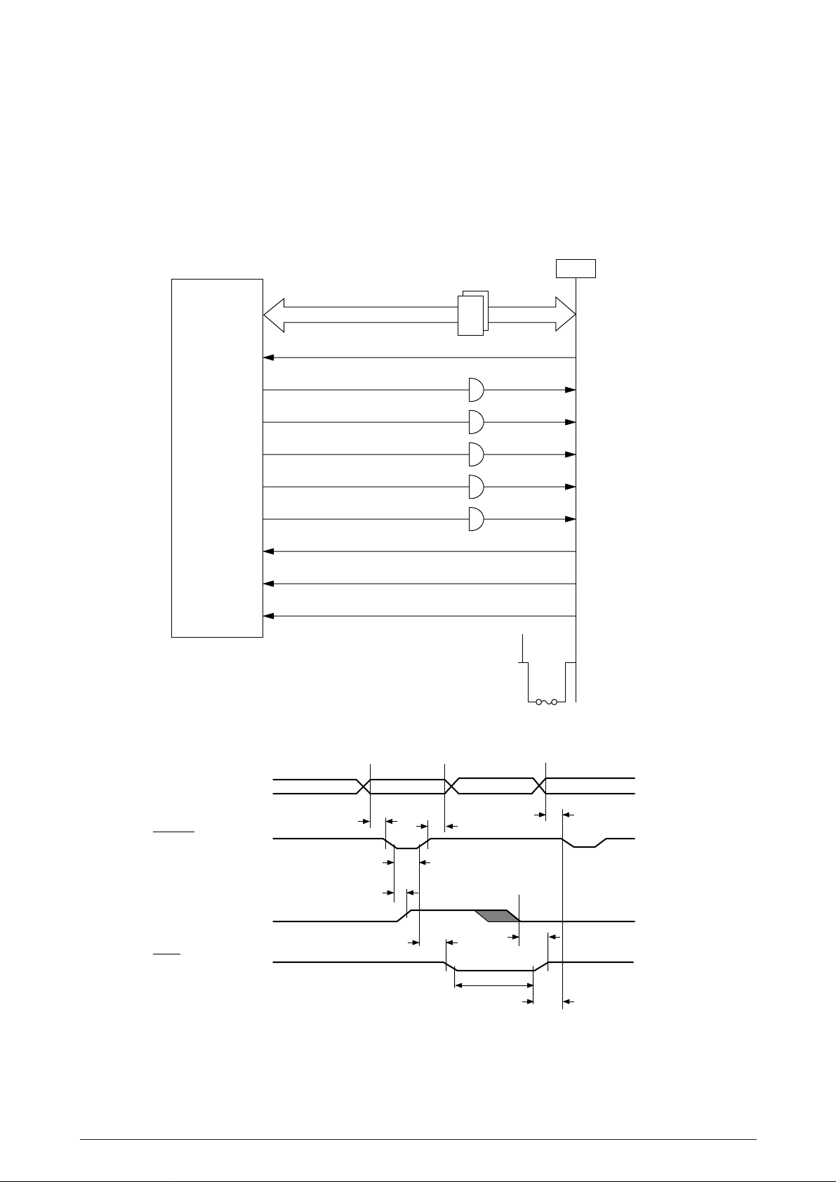
3.3.2 Video I/F
Video data is sent from PCR in synchronization with WCLK sent from PX 4
When PX4 is in ready status (PRDY = Low), PCR gives a printing start instruction to PX4 by PRINT
Low Plus or command to send an extracted video data. When receiving the printing start
instruction, PX4 becomes BUSY status (PRDY=High) and starts a paper hopping. After the paper
reached the specified position, PX4 sends each FSYNC of WCLK, LSYNC and YMCK.
FSYNC becomes enabled due to its tandem structure, synchronizing with the pass of a paper
through each ID.
If PX 4 becomes enabled to receive next page video data during printing the first page, it sets PRDY
to Low and returns to Ready status.
For 4-color video data, 4 colors are sent through 1 line in 8 bit width in synchronization with LSYNC.
4 patterns of status of COL1,_ indicate which YMCK the currently sent data is. The color data is
sent in accordance with each status by changing COL1,_ 4 times at one LSYNC. Even when
FSYNC is disabled, the sending mode of each color exists only for the specified WCLK, but the
sending of video data won’t be executed.
IMEM
µ
PD94704
WDATA7-N
~
WDATA0-N
COL1-N
COL0-N
WCLK-N
LSYNC-N
FSYNCY-N
FSYNCM-N
FSYNCC-N
FSYNCK-N
PX4-PCBPCR-PCB
+5V
IC13
88
16244
IC13
EM1
+5V
+5V
x 8
x 8
IC1
MB87D113PFV
(LSI)
WDATA7
~
WDATA0
COL1
COL0
WCLK
LSYNC
FSYNCY
FSYNCM
FSYNCC
FSYNCK
IIF
µ
PD66044
PRINT-N
PRDY-N
40985501TH Rev.1 43 /
IC20
IC20
IC10
M65524
(CPU)
PRDY
Page 44

PRINT
g
PRDY
FSYNCY
FSYNCM
FSYNCC
FSYNCK
LSYNC
COL1
COL2
WDATA0~7
WCLK
Print interval for one page
Drum one sycle or more, including heater warm up time (MAX. 60min.)
Under 4-color printin
LSYNC
COL0
COL1
WDATA0~7
WCLK
WCLK
LSYNC
WDATA0~7
Enlarged chart for 4-color printing
Y=00 M=01 C=10 K=11
YDATA MDATA CDATA KDATA YDATA MDATA CDATA KDATA
1 line 4-color data
40985501TH Rev.1 44 /
Page 45

3.3.3 Command Interface
(1) Command Interface Time Chart
Power on
Communication enabled status
PPRDY
*1
CPRDY
*1
CBSY
Command
SBSY
MSB LSB MSB LSB
SC
SCLK
*2
Status
*1 For timing to set PPRDY and CPRDY to on, which of them is earlier is not specified.
After powering on, they are set to on when the initial process is completed and they are
changed to the communication enabled status. Therefore, at the point when PPRDY and
CPRDY are set to on, the communications are to become the enabled status.
*2 SCLK should be 50% DUTY.
40985501TH Rev.1 45 /
Page 46

(2) Controlling Command Interface
a) Under regular operation
CU sets CBSY to ON and sends a command to PU. At this time, PU section sends clock
signals and CU recognizes the completion of command sending by receiving 8 clock
signals. And CU returns CBSY to OFF.
Next, PU sets SBSY to ON and sends a reply for the command it receives. At this time,
PU sends clock signals and returns SBSY to OFF in the same way. CU recognizes the
completion of the reply receiving by receiving 8 clock signals.
If the completion of sending or receiving cannot be recognized for a fixed time, a command
is retransmitted. Therefore, a timer is provided for monitoring the completion of
communication, and started when a command is sent and stopped when the receiving is
completed.
The value for timer should be determined from higher values than T max. value in the
following figure.
timer timer stop timer
CBSY
Sending completed
SBSY
Receiving completed
T max.
T max= 19ms
40985501TH Rev.1 46 /
Page 47

b) Under irregular operation-1 (when a command sending is not normally performed)
When CU sends a command to PU and a noise or hardware malfunction causes to skip
clock sending, CU cannot recognize the completion of sending, so CBSY is left ON.
Therefore, return CBSY to OFF once by the time-out of timer described in (1), and after
time compensation for T min., retry the sending and receiving sequence by retransmitting
the command.
When the communication cannot be succeeded by the first retry, execute the second retry.
When the second retry cannot succeed, some message is indicated to the operator and
the system is to be shut down.
Note: Since the PU section cannot recognize the skip of the clock, an irregular
command from CU is processed as it is, and when CBSY is set to OFF, a reply
for the command is returned. Thus, for CU section, a reply is returned even
though the sending cannot be completed, so it must receive and flush the
reply.
timer
CBSY
Sending completed
SBSY
Receiving completed
c) Under irregular operation -2 (When a reply receiving is not normally performed)
When PU returns a reply to CU and a noise or hardware malfunction causes to skip clock
sending, CU cannot recognize the completion of receiving. Therefore, retransmit the
command by the time-out described in (1) and retry the sending and receiving sequence.
When the communication cannot be succeeded by the first retry, execute the second retry.
When the second retry cannot succeed, some message is indicated to the operator and
the system is to be shut down.
timer timer
CBSY
time-out
retry
T min
time-out
retry
timer
Sending completed
SBSY
Receiving completed
40985501TH Rev.1 47 /
Page 48

4. TROUBLESHOOTING
4.1 Troubleshooting Table
Normal operation
When powered on, the page printer
turns on LEDs for about one sec-
ond to check whether the LEDs and
the LCD are normal.
Normal operation
Normal operation
Normal operation
Normal operation
Normal operation
Normal operation
To clear this message, press the
RESET switch.
To clear this message, press the
RESET switch.
Normal operation
Normal operation
When “CLEARABLE WARNINGS”
on the menu is set to “ON”, press
the RECOVER switch to clear the
message.
Normal operation
Displayed when the page printer is powered on.
Table 4.1 Status and alarm indication list
Undefined Undefined Undefined Undefined ON OFF
Displayed while the controller is initializing (after the
page printer is powered on).
The printer is in the on-line mode.
The printer is in the off-line mode.
Undefined Undefined Undefined Undefined OFF OFF
Undefined Undefined Undefined Undefined ON Undefined
Undefined Undefined Undefined Undefined OFF Undefined
Displayed while the page printer is printing.
Displayed while the page printer is receiving data
or performing the output processing.
Indicates that the data remains unprinted in the
buffer.
This message is displayed data remain unprinted
in the buffer (offline). This message prompts the
user to press the RESET switch, if cancel the data.
This message prompts the user need to press the
RESET switch before writing the new menu setting
in EEPROM.
This message is displayed when the printer cannot
reset automatically as there remain data and tem-
porary attributes (DLL, macro, user patter, or user
symbol set) .
Indicates that the data (to the end of processing) is
Undefined Undefined Undefined Undefined Undefined Undefined
Undefined Undefined Undefined Undefined Blink Undefined
Undefined Undefined Undefined Undefined Undefined Undefined
Undefined Undefined Undefined Undefined ON Undefined
Undefined Undefined Undefined Undefined OFF OFF
Undefined Undefined Undefined Undefined Blink OFF
being canceled.
Indicates that a printer language which is not avail-
able has been specified by the PJL command.
Undefined Undefined Undefined Undefined Undefined Undefined
Displays the number of a copies being printed out
when the number of copies being printed is two or
more.
Undefined Undefined Undefined Undefined Undefined Undefined
ttttt
ttttt
Message K C M Y READY ATTENTION Trouble or Status Remedy
INITIALIZING
ON-LINE . xxx
OFF-LINE . xxx
PRINTING
PROCESSING . xxx
DATA PRESENT. xxx
RESET TO FLUSH
Category LCD Status LED
Daily status
40985501TH Rev.1 48 /
RESET TO SAVE
FLUSHING JOB
PS NOT AVAILABLE
COPY nnn/mmm
Page 49

This massage is cleared when the
drum is properly positioned or
sensor lever which is exchanged
correspond to the LED color lights.
Normal operation
Normal operation
This message is cleared when the
toner cartridge is replaced.
Normal operation
This message is cleared when the
specified drum is replaced.
Indicates that Toner sensor is abnormal when page
counter is above thirty . (The LED of the color lights)
Indicates that the page printer enters the Power
Save mode (in which the heater is powered off).
Indicator that the toner of the specified color is
running out. However, when “LOW TONER” is set
to “OFF,” the ATTENTION indicator blinks.
Indicates that the life of a specified color drum has
come.
(The LED of the color lights.)
After the drum is replaced, its drum
counter must be reset. (See the us-
er’s manual.)
Normal operation
This message is cleared when the
Heat unit Assy is replaced. After the
Heat unit Assy is replaced, its
counter must be reset. (See the
user’s manual.)
Normal operation
This message is cleared when the
Indicates that the life of the Heat unit Assy has come.
Indicates that the life of the belt cassette Assy has
come.
belt cassette assembly is replaced.
After the belt cassette assembly is
replaced, its counter must be reset.
(See the user’s manual.)
Normal operation
Cleans the data left unprinted in the buffer and ini-
tializes the printer to the user default status. The
Normal operation
temporary DLL, macro, and user patterns are de-
leted.
Prints out a demo page.
This operation is started by a command when the
READY LED is on or by a switch when the READY
LED is blinking.
ON ON ON ON Undefined ON
Message K C M Y READY ATTENTION Trouble or Status Remedy
TNR SNS *******
Category LCD Status LED
Daily status
40985501TH Rev.1 49 /
ON ON ON ON Undefined ON or Blink
Undefined Undefined Undefined Undefined Undefined Undefined
POWER SAVING
TNR LOW *******
ON ON ON ON Undefined ON
CNG DRUM *******
Undefined Undefined Undefined Undefined Undefined ON
FUSER LIFE
Undefined Undefined Undefined Undefined Undefined ON
BELT LIFE
OFF OFF OFF OFF OFF OFF
RESET
Undefined Undefined Undefined Undefined Blink or ON Undefined
PRINT DEMO PAGE
Page 50

Normal operation
Prints out a menu setting.
This operation is started by a command when the
This massage is cleared when the oil
roller assy is replaced. After the oil roller
assy is replaced, its counter must be
reset. (See the user’s manual)
Normal operation
READY LED is on or by a switch when the READY
LED is blinking.
Indicates that the life of the Oil roller assy has come.
(Warning)
Indicates that the life of the Oil roller assy has come.
(Alarm)
Prints out all character sets (fonts) that the page
printer contains.
This operation is started by a command when the
This message temporarily disap-
pears when a cover of the page
printer is opened but will be dis-
READY LED is on or by a switch when the READY
LED is blinking.
Displayed when 50 pages are printed after “Toner
Low” was detected to prompt the user to replace
the toner cartridge.
played every 20 pages unless the
cartridge is replaced.
This error is reset when the box
toner Assy is replaced. Printing is
suppressed until it is replaced.
The front feeder becomes not avail-
able when the RECOVER switch is
pressed. The other tray is available.
This message is cleared when the
front feeder assembly is replaced.
This error is reset when the cover is
closed. If this error occurs fre-
quently, go to 6.5.2.
This error is recovered when the belt
Displayed when 100 pages are printed after “Box
toner Assy Full” was detected to prompt the user to
replace the box toner Assy.
Indicates that the front feeder has caused a home
position error.
Indicates that the printer covers is open.
Indicates that the belt cassette Assy has not been
cassette Assy is installed. Printing
is suppressed until the belt cassette
assembly is installed.
installed.
Undefined Undefined Undefined Undefined Blink or ON Undefined
Message K C M Y READY ATTENTION Trouble or Status Remedy
PRINT MENU
Category LCD Status LED
Daily status
40985501TH Rev.1 50 /
Undefined Undefined Undefined Undefined Undefined ON
Undefined Undefined Undefined Undefined OFF Blink
Undefined Undefined Undefined Undefined Blink or ON Undefined
OIL ROLLER LIFE
OIL ROLLER LIFE
PRINT FONTS
Blink Blink Blink Blink OFF Blink
*******
TONER EMPTY
Undefined Undefined Undefined Undefined OFF Blink
WASTE TONER FULL
Undefined Undefined Undefined Undefined OFF Blink
FRONT TRAY ERROR
PRESS
RECOVERKEY
Undefined Undefined Undefined Undefined OFF Blink
COVER OPEN
Undefined Undefined Undefined Undefined OFF Blink
BELT NOT
INSTALLED
Page 51

This error is recovered when the box
toner Assy is installed. Printing is
suppressed until the box toner
assembly is installed.
Nothing
Please install the Oil pad Assy.
This error is recovered when the
RECOVER switch is pressed.
Expand RAM or reduce data.
Indicates that the box toner Assy has not been
installed.
Indicates that the Box toner Assy is near full.
Indicates that the Oil pad Assy has not been
installed.
Indicates that data overflowed the memory space.
- Too much print data in one page
- Too much macro data
- Too much DLL data
This error is recovered when the
RECOVER switch is pressed.
Change the setting of Receive
Buffer Size in the User Maintenance
more bigger then send the data from
the host or expand RAM.
This message is cleared when pa-
per is set in the tray or the cassette
assembly is mounted.
- Data overflow after compression of frame data
Indicates that the receive buffer was overflowed.
Indicates that the tray is empty or the cassette as-
sembly has not been installed.
mm...m: paper size (Letter, Executive, Legal 14,
The second tray (optional) cannot
use A6-size paper. The A6-size
paper is available to the first tray or
to the front feeder.
Legal 13, A4, A5, A6, or B5 size)
tttttt: Tray type (Tray 1, Tray 2, or Front)
Displayed when the second tray (optional) contains
A6-size paper.
This message is cleared when the
first tray is remounted correctly.
Normal operation
This message is cleared when the
specified paper is loaded from
manual feeder.
Indicates that the first tray is pulled out also when
the second tray (optional) is used.
Requests the user to load the specified paper by
message from manual feeder.
mm...m: paper size (Letter, Executive, Legal 14,
Legal 13, A4, A5, A6, or B5 size)
Undefined Undefined Undefined Undefined OFF Blink
Message K C M Y READY ATTENTION Trouble or Status Remedy
WASTE TONER BOX
NOT INSTALLED
Category LCD Status LED
Daily status
40985501TH Rev.1 51 /
Undefined Undefined Undefined Undefined Undefined ON
Undefined Undefined Undefined Undefined OFF Blink
WASTE TNR NRFULL
OIL P AD NOT
Undefined Undefined Undefined Undefined OFF Blink
INSTALLED
ERROR MEMORY
OVERFLOW
Buffer
Overflow
Undefined Undefined Undefined Undefined OFF Blink
ERROR RECEIVE
BUFFER OVERFLOW
Undefined Undefined Undefined Undefined OFF Blink
PAPER OUT
mmmmmmmmm tttttt
Tray Paper
Out
Undefined Undefined Undefined Undefined OFF Blink
CANNOT USE A6
Undefined Undefined Undefined Undefined OFF Blink
Undefined Undefined Undefined Undefined ON OFF
PAPER ON TRAY 2
TRAY 1 INSTALL
mmmmmmm MANUAL
P APER REQUEST
Paper
Request
Page 52

Normal operation
This message is cleared when pa-
per is set in the specified tray.
Requests the user to load the specified paper in the
tray .
mm...m: paper size (Letter, Executive, Legal 14,
Check the size of paper in the tray
or whether two or more paper
sheets are fed at a time.
When the cover is opened and
closed, this error is reset and print-
ing resumes. If this error occurs fre-
quently, go to 6.5.2.
Check the size of paper in the tray
or whether two or more paper
sheets were fed at a time. When
the cover is opened and closed, this
error is reset and printing resumes.
Legal 13, A4, A5, A6, or B5 size)
tttttt: Tray type (Tray 1, Tray 2, or Front)
Indicates that paper of the illegal size was fed from
the specified tray.
tttttt: Tray type (Tray 1, Tray 2, or Front)
Indicates that a paper jam occurred on the paper
feeding from the specified tray.
tttttt: Tray type (Tray 1, Tray 2, or Front)
If this error occurs frequently, go to
6.5.2.
Check the size of paper in the tray
or whether two or more paper
sheets were fed at a time. When
the cover is opened and closed, this
error is reset and printing resumes.
If this error occurs frequently, go to
6.5.2.
Open the cover and remove a pa-
per jam from the inside of the page
printer. When the cover is opened
and closed, this error is reset and
printing resumes. If this error oc-
curs frequently, go to 6.5.2.
The page printer recovers automati-
cally when resetting is complete.
Indicates that a paper coming out of the tray jammed
on the paper traveling printer.
tttttt: Tray type (Tray 1, Tray 2, or Front)
Indicates that a paper jammed on the way to the
exit.
Indicates that the OKI HSP interface card is being
reset.
Undefined Undefined Undefined Undefined OFF Blink
Message K C M Y READY ATTENTION Trouble or Status Remedy
mmmmmmmmm tttttt
PAPER REQUEST
Category LCD Status LED
Paper
Request
40985501TH Rev.1 52 /
Undefined Undefined Undefined Undefined OFF Blink
ERROR P APER SIZE
CHECK tttttt
Paper Size
Error
Undefined Undefined Undefined Undefined OFF Blink
PAPER INPUT JAM
CHECK tttttt
Paper Jam
Error
Undefined Undefined Undefined Undefined OFF Blink
PAPER FEED JAM
CHECK tttttt
Undefined Undefined Undefined Undefined OFF Blink
PAPER EXIT JAM
REMOVE THE PA-
PER
Undefined Undefined Undefined Undefined OFF Blink
OKI HSP I/F CARD
RESETTING
Interface
Error
Page 53

Notifies that the power supply LSI
has been reset due to noise, etc.
(process error)
Open cover and remove the paper.
Close cover to recover and proceed.
The page printer recovers from the
error when the RECOVER switch is
pressed. If this error occurs fre-
quently, replace the OKI HSP inter-
face card or the main board (PCR
PCB).
printer is powered on.
mode starts or the page printer received a
Indicates that Process error occurred.
Indicates that a fatal OKI HSP interface error has
occurred.
xx=10: Interface timeout
xx=20: Initialization failed 10 seconds after the page
xx=21: It takes 3 seconds or more before the RUN
Sets the default values in EEPROM
and it’ll be recovered automatically.
Simplify the pages.
Run Mode command in the power-on mode.
xx=22: HSP-PC communication error
Indicates that the ID number of EEPROM is invalid.
Indicates that the interpreter detected one of the
errors given below . The data coming after this error
is recovered until the end of the command. When
the reception of the command is completed, this
message is reset automatically.
is full.
- Invalid PostScript command
- The page is complicated and the vertical memory
Undefined Undefined Undefined Undefined OFF Blink
Message K C M Y READY ATTENTION Trouble or Status Remedy
Jam 001
Error
Category LCD Status LED
Interface
Error
40985501TH Rev.1 53 /
Undefined Undefined Undefined Undefined OFF Blink
ERROR HOST I/F
OKI HSP xx
Undefined Undefined Undefined Undefined OFF Blink
Undefined Undefined Undefined Undefined Blink OFF
EEPROM
RESETTING
ERROR POSTSCRIPT
Controller
Error
Page 54

Remedy
Turn on the power of the page printer again.
If this error still occurs, replace the program
ROM on the main board (PCR PCB) or the
main board itself.
When replacing the main board (PCR PCB),
demount the EEPROM chip from the old main
board and remount it on the new main board.
Turn on the power of the page printer again.
If this error still occurs, replace the main board
(PCR PCB).
When replacing the main board (PCR PCB),
demount the EEPROM chip from the old main
Indicates that an error was found
in the program ROM by the pro-
gram ROM check.
Indicates that an error was found
in the resident RAM by the resi-
dent RAM check.
board and remount it on the new main board.
Turn on the power of the page printer again.
If this error still occurs, replace the program
ROM on the main board (PCR PCB) or the
main board itself.
When replacing the main board (PCR PCB),
demount the EEPROM chip from the old main
board and remount it on the new main board.
Turn on the power of the page printer again.
If this error still occurs, replace the optional
ROM on the main board (PCR PCB) or the
main board itself.
When replacing the main board (PCR PCB),
demount the EEPROM chip from the old main
board and remount it on the new main board.
Check the connection of the option RAM. Turn
Indicates that an error was found
in the EEPROM by the EEPROM
check.
Indicates that an error was found
in the optional ROM by the optional
ROM check.
Indicates that an error was found
on the power of the page printer again. If this
error still occurs, replace the main board (PCR
PCB) or the option RAM.
When replacing the main board (PCR PCB),
demount the EEPROM chip from the old main
board and remount it on the new main board.
Do not use this SIMM because it is
incompatible with the machine.
in the optional RAM by the optional
RAM check.
Indicates that an error in the allocation
to CAS and data bus, which is detected
from the results of 1byte write/ 8bytes
read check on the optional RAM.
10
(nn)
Code
Undefined Undefined Undefined Undefined OFF Blink Details of error
30
40
50
60
61
Message K C M Y READY ATTENTION Trouble or Status Remedy
ERROR
nn
Category LCD Status LED
Controller
Error
40985501TH Rev.1 54 /
Page 55

Remedy
This massage is cleared when the drum is
properly positioned or sensor lever which is
exchanged correspond to the LED color lights.
Check the connection between the main
board and the operation panel. Turn on the
power of the page printer again. If this error
still occurs, replace the cable, the main board
(PCR PCB) or the cover assembly operation
panel.
When replacing the main board (PCR PCB),
demount the EEPROM chip from the old main
Details of error
Indicates that Toner sensor is
abnormal when page counter is
below thirty.(alarm)
Indicates that a timeout occurred
on interface between the page
printer and the operator panel.
Check the connection between the main
board and the engine board. Turn on the
power of the page printer again. If this error
still occurs, replace the program ROM of the
main board (PCR PCB) or the engine board
(PX4 PCB), or the board itself.
When replacing the main board (PCR PCB),
demount the EEPROM chip from the old main
board and remount it on the new main board.
See Chapter 6.5.2
See Chapter 6.5.2
board and remount it on the new main board.
Indicates that a timeout occurred
on CU-PU interface.
Indicates that the printer overruns.
See Chapter 6.5.2
Yellow Image drum unit up/down
error
Magenta Image drum unit up/down
error
C. If this condition is not
°
See Chapter 6.5.2
Cyan Image drum unit up/down
error
Black Image drum unit up/down
error
satisfied, adjust the surrounding temperature,
otherwise satisfied, replace the sensor board
(RXM-PCB), junction board (PXF-PCB) or
Make sure that the surrounding temperature
stays -10 < t< 50
Environment temperature sensor
error
engine board (PX4-PCB).
(nn)
Code
Blink Blink Blink Blink OFF Blink
77
80
Undefined Undefined Undefined Undefined OFF Blink
82
92
Blink Blink Blink Blink OFF Blink
D6
Undefined Undefined Undefined Undefined OFF Blink
D7
D8
D9
DA
Message K C M Y READY ATTENTION Trouble or Status Remedy
ERROR
nn
Category LCD Status LED
Controller
Error
40985501TH Rev.1 55 /
Page 56

Remedy
Make sure that the relative humidity stays 0%
< h < 95%. (the subsequent contents are the
same as those of [DA])
Re-mount the waste toner box and re-power
on to ensure whether the alarm goes off or
not. If the alarm stays on, exchange waste
toner sensor, or replace the junction board
(PXF-PCB) or engine board (PX4-PCB).
Turn on the power of the page printer again.
If this error still occurs, replace the engine
board (PX4 PCB) or the front feed assembly.
See Chapter 6.5.2
See Chapter 6.5.2
Check the connection between the engine
board and the second tray board. Turn on
the power of the page printer again. If this
error still occurs, replace the program ROM
of the engine board (PX4 PCB), the junction
board (PXF PCB), the second tray board
(AOLT PCB).
When replacing the main board, demount the
EEPROM chip from the old main board and
remount it on the new main board.
Turn on the power of the page printer again.
If this error still occurs, replace the program
ROM of the engine board (PX4 PCB) or the
engine board.
When replacing the main board, demount the
EEPROM chip from the old main board and
remount it on the new main board.
Turn on the power of the page printer again.
If this error still occurs, replace the power
supply board (power-supply PCB).
Humidity sensor error
DB
(nn)
Code
Waste-toner sensor error
DC
Pinch roller up/down error
DE
Fusing Unit Error
Fan Motor Error
Option status error 2 (Error on in-
terface between the engine board
and the second tray)
E0E1E8
SRAM error
E9
PW-LSI error
EA
Undefined Undefined Undefined Undefined OFF Blink Details of error
Message K C M Y READY ATTENTION Trouble or Status Remedy
ERROR
nn
Category LCD Status LED
Controller
Error
40985501TH Rev.1 56 /
Page 57

Remedy
Turn on the power of the page printer again.
If this error still occurs, replace the program
ROM of the engine board (PX4 PCB) or the
engine board.
When replacing the main board, demount the
EEPROM chip from the old main board and
remount it on the new main board.
Turn on the power of the page printer again.
If this error still occurs, replace the EEPROM
of the engine board (PX4 PCB) or the engine
board.
When replacing the main board, demount the
EEPROM chip from the old main board and
remount it on the new main board.
Turn on the power of the page printer again.
If this error still occurs, replace the EEPROM
of the engine board (PX4 PCB) or the engine
board.
When replacing the main board, demount the
EEPROM chip from the old main board and
remount it on the new main board.
Turn on the power of the page printer again.
If this error still occurs, replace the program
ROM of the engine board (PX4 PCB) or the
engine board.
When replacing the main board, demount the
EEPROM chip from the old main board and
remount it on the new main board.
Turn on the power of the page printer again.
If this error still occurs, replace the program
ROM of the main board (PCR PCB) or the
main board.
When replacing the main board, demount the
EEPROM chip from the old main board and
remount it on the new main board.
Engine firmware lost control
(nn)
EC
Code
EEPROM error (Timeout)
ED
EEPROM error (Not Exist)
EE
Engine ROM/RAM error
EF
Monitor error (Double wait)
F0
Undefined Undefined Undefined Undefined OFF Blink Details of error
Message K C M Y READY ATTENTION Trouble or Status Remedy
ERROR
nn
Category LCD Status LED
Controller
Error
40985501TH Rev.1 57 /
Page 58

Remedy
Turn on the power of the page printer again.
If this error still occurs, replace the program
ROM of the main board (PCR PCB) or the
main board.
When replacing the main board, demount the
EEPROM chip from the old main board and
remount it on the new main board.
Turn on the power of the page printer again.
If this error still occurs, replace the program
ROM of the engine board (PX4-PCB) or the
engine board.
Monitor error (Argument error)
F1
(nn)
Code
Engine background error
F4
Undefined Undefined Undefined Undefined OFF Blink Details of error
Message K C M Y READY ATTENTION Trouble or Status Remedy
ERROR
nn
Category LCD Status LED
Controller
Error
40985501TH Rev.1 58 /
Page 59

Remedy
If the error still occurs, replace the
main board (PCR PCB).
When replacing the main board,
demount the EEPROM chip from
the old main board and remount it
Turn on the power of the page printer
again. The error will be reset.
Details of error
TLB (Translation Lookaside Buffer) correc-
tion exception
TLB exception (Load or Instruction Fetch)
01
(nn)
Code
Indicates that the controller error has occurred.
020304
on the new main board.
TLB exception (Store)
Address error exception (Load or Instruc-
tion Fetch)
Address error exception (Store)
Bus error exception (Instruction Fetch)
Bus error exception (Data Load or Store)
System call exception
Break point exception
Reserved instruction exception
0506070809
0A0B0C0D0FB0B1
Co-processor disabled exception
Operation overflow exception
Trap exception
Floating-point exception
NMI: Hardware breakpoint
NMI: Write protect
Cache error
C0
Undefined Undefined Undefined Undefined OFF Blink
Message K C M Y READY ATTENTION Trouble or Status Remedy
ERROR
CONTROLLER
nn-aaaaaaaa
Category LCD Status LED
Controller
Error
40985501TH Rev.1 59 /
Page 60

4.2 Troubleshooting Flowchart
A-1 PS NOT AVAILABLE.
• Is the PS-SIMM properly installed?
• No Exchange the PSIMMH with the PSIMML of SIMMs.
▼
• Yes See the items of ERROR 50?
A-2 ERROR POSTSCRIPT.
• See the items of ERROR 50?
A-3 ERROR MEMORY OVERFLOW.
• Dose the capacity of the installed memory correspond with that shown in the Menu
Print page?
• Yes Replace the memory with a larger one than it.
▼
• No See the items of ERROR 50.
A-4 ERROR RECEIVE BUFFER OVERFLOW.
• See the items of ERROR.
A-5 OKI HSP I/F CARD RESETTING.
• Can the machine return to On-line mode in a few minutes?
• Yes No abnormality.
▼
• No Replace the HSP I/F CARD.
▼
• Can the machine recover to a normal state?.
▼
• No Replace the PCR board.
40985501TH Rev.1 60 /
Page 61

A-6 ERROR HOST I/F OKI HSP xx.
• Is the FU1 burnt?
• Yes Replace the FU1.
▼
• No Replace the R550 to R555.
▼
• Can the machine recover to a normal state?
• No Replace the MUPIS connector.
▼
• Can the machine recover to a normal state?
• No Replace the IC21 to IC26.
▼
• Can the machine recover to a normal state?
• No Replace the IIF
▼
• Can the machine recover to a normal state?
▼
• No Replace the PCR board.
B-1 ERROR 10
• Is the ROM inserted into its specified position?
• No Reinstall the ROM in place.
▼
• Yes Replace the ROM.
▼
• Can the machine recover to a normal state?
▼
• No Replace the PCR board.
B-2 ERROR 30.
• Replace R501 and / or R502.
▼
• Can the machine recover to a normal state?
• No Replace DRAM01 to DRAM04 and DRRAM11 to DRAM14.
▼
• Can the machine recover to a normal state?
• No Replace the IC5 to IC8, IC11 and IC12.
▼
• Can the machine recover to a normal state?
▼
• No Replace the PCR board.
40985501TH Rev.1 61 /
Page 62

B-3 ERROR 40.
• Replace the E2ROM1.
▼
• Can the machine recover to a normal state?
• No Replace the R566.
▼
• Can the machine recover to a normal state?
• No Replace the SIMM socket of the PSIMMH.
▼
• Can the machine recover to a normal state?
▼
• No Replace the PCR board.
B-4 ERROR 50.
• Is the PSIMM properly inserted in its specified position?
• No Reinstall the SIMM accurately.
▼
• Yes Replace the SIMM.
▼
• Can the machine recover to a normal state?
• No Replace the IC1 to IC4, IC9 and IC10.
▼
• Can the machine recover to a normal state?
▼
• No Replace the PCR board.
B-5 ERROR 60.
• Is the capacity/ access speed of the two SIMMs the same?
• No Install a SIMM for one of the pair with the same capacity/ access speed
▼
• Yes Are the SIMMs installed properly?
• No Reinstall the SIMM(s) in place.
▼
• Yes Replace the SIMM(s).
▼
• Can the machine recover to a normal state?
• No Replace the IC5 to IC8, IC11 and IC12.
▼
• Can the machine recover to a normal state?
as the othe one.
▼
• No Replace the PCR board.
40985501TH Rev.1 62 /
Page 63

B-6 ERROR 80.
• Replace the IC9.
▼
• Can the machine recover to a normal state?
• No Replace the IIF.
▼
• Can the machine recover to a normal state?
• No Replace the PANEL connector.
▼
• Can the machine recover to a normal state?
• No Replace the PCR board.
▼
• Can the machine recover to a normal state?
• No Replace the cable Assy of the Operator Panel.
▼
• Can the machine recover to a normal state?
▼
• No Replace the Operator Panel Assy.
B-7 ERROR 82.
• Replace the IC8 and/ or IC20.
▼
• Can the machine recover to a normal state?
• No Replace the IIF.
▼
• Can the machine recover to a normal state?
• No Replace the PU connector.
▼
• Can the machine recover to a normal state?
• No Replace the PCR board.
▼
• Can the machine recover to a normal state?
▼
• No Replace the PX4.
B-8 ERROR 92.
• Replace the PCR board.
B-9 ERROR F4.
• See the items of ERROR 60.
B-10 ERROR COTROLLER xx.
• Replace the PCR board.
40985501TH Rev.1 63 /
Page 64

C-1 The Operator Panel displays nothing with the upper line blackened.
• Replace the IRST.
▼
• Can the machine recover to a normal state?
• No Replace the PANEL connector.
▼
• Can the machine recover to a normal state?
• No Replace the cable Assy of the Operator Panel.
▼
• Can the machine recover to a normal state?
• No Replace the Operator Panel Assy.
▼
• Can the machine recover to a normal state?
• No Replace the PCR board.
▼
• Can the machine recover to a normal state?
• No Replace the PX4 board.
▼
• Can the machine recover to a normal state?
▼
• No Replace the power supply.
C-2 The Operator Panel displays an abnormal message.
• See the items of ERROR 80.
C-3 The machine refuses the operations to switching on the Operator Panel.
• Replace the R587.
▼
• Can the machine recover to a normal state?
▼
• See items of ERROR 80.
40985501TH Rev.1 64 /
Page 65

D-1 No receiving trough the centronics I/F.
• Replace the R595, R664, R594, R597, R663, R596, R648 and R55.
▼
• Can the machine recover to a normal state?
• No Replace the C3 and/ or C52.
▼
• Can the machine recover to a normal state?
• No Replace the IC16 and IC17.
▼
• Can the machine recover to a normal state?
• No Replace the CENT connector.
▼
• Can the machine recover to a normal state?
• No Replace the IIF.
▼
• Can the machine recover to a normal state?
• No Replace the PCR board.
40985501TH Rev.1 65 /
Page 66

5. CIRCUIT DIAGRAM
Figure 5-1(1/15~15/15) Main Controller PCB (PCR-PCB, Rev.2, 3)
Figure 5-2(1/3~3/3) Operation Panel PCB (PCO-PCB, Rev.2)
Figure 5-3(1/1) PostScript SIMM PCB (Used Flash ROM) (FSL-PCB, Rev.1)
Figure 5-4(1/1) PostScript SIMM PCB (Used OTP or Mask ROM) (MSM-PCB, Rev.1)
Figure 5-5(1/9~9/9) Engine Controller-PCB (PX4-PCB, Rev.2)
Figure 5-6(1/2~2/2) I/F-PCB (PXF-PCB, Rev.4)
Figure 5-7(1/1) Head I/F-PCB (PD6-PCB, Rev.3)
Figure 5-8(1/2~2/2) Front Sensor-PCB (PXM-PCB, Rev.3)
Figure 5-9(1/2~2/2) Rear Sensor-PCB (PXL-PCB, Rev.3)
Figure 5-10(1/1) Cassette Switch-PCB (PXC-PCB, Rev.3)
40985501TH Rev.1 66 /
Page 67

123 45678 9XY
123 45678 9XY
A
B
C
D
E
F
G
H
A
B
C
D
E
F
G
H
(PCR-1/15) Rev. 2, 3
Figure 5-1 Main Control PCB
40985501TH Rev.1 67 /
Page 68

123 45678 9XY
123 45678 9XY
A
B
C
D
E
F
G
H
A
B
C
D
E
F
G
H
(PCR-2/15) Rev. 2, 3
Figure 5-1 Main Control PCB
40985501TH Rev.1 68 /
Page 69

123 45678 9XY
123 45678 9XY
A
B
C
D
E
F
G
H
A
B
C
D
E
F
G
H
(PCR-3/15) Rev. 2, 3
Figure 5-1 Main Control PCB
40985501TH Rev.1 69 /
Page 70

123 45678 9XY
123 45678 9XY
A
B
C
D
E
F
G
H
A
B
C
D
E
F
G
H
(PCR-4/15) Rev. 2, 3
Figure 5-1 Main Control PCB
40985501TH Rev.1 70 /
Page 71

123 45678 9XY
123 45678 9XY
A
B
C
D
E
F
G
H
A
B
C
D
E
F
G
H
(PCR-5/15) Rev. 2, 3
Figure 5-1 Main Control PCB
40985501TH Rev.1 71 /
Page 72

123 45678 9XY
123 45678 9XY
A
B
C
D
E
F
G
H
A
B
C
D
E
F
G
H
(PCR-6/15) Rev. 2, 3
Figure 5-1 Main Control PCB
40985501TH Rev.1 72 /
Page 73

123 45678 9XY
123 45678 9XY
A
B
C
D
E
F
G
H
A
B
C
D
E
F
G
H
(PCR-7/15) Rev. 2, 3
Figure 5-1 Main Control PCB
40985501TH Rev.1 73 /
Page 74

123 45678 9XY
123 45678 9XY
A
B
C
D
E
F
G
H
A
B
C
D
E
F
G
H
(PCR-8/15) Rev. 2, 3
Figure 5-1 Main Control PCB
40985501TH Rev.1 74 /
Page 75

123 45678 9XY
123 45678 9XY
A
B
C
D
E
F
G
H
A
B
C
D
E
F
G
H
(PCR-9/15) Rev. 2, 3
Figure 5-1 Main Control PCB
40985501TH Rev.1 75 /
Page 76

123 45678 9XY
123 45678 9XY
A
B
C
D
E
F
G
H
A
B
C
D
E
F
G
H
47
47
(PCR-10/15) Rev. 2, 3
Figure 5-1 Main Control PCB
40985501TH Rev.1 76 /
Page 77

123 45678 9XY
123 45678 9XY
A
B
C
D
E
F
G
H
A
B
C
D
E
F
G
H
(PCR-11/15) Rev. 2, 3
Figure 5-1 Main Control PCB
40985501TH Rev.1 77 /
Page 78

123 45678 9XY
123 45678 9XY
A
B
C
D
E
F
G
H
A
B
C
D
E
F
G
H
(PCR-12/15) Rev. 2, 3
Figure 5-1 Main Control PCB
40985501TH Rev.1 78 /
Page 79

123 45678 9XY
123 45678 9XY
A
B
C
D
E
F
G
H
A
B
C
D
E
F
G
H
(PCR-13/15) Rev. 2, 3
Figure 5-1 Main Control PCB
40985501TH Rev.1 79 /
Page 80

123 45678 9XY
123 45678 9XY
A
B
C
D
E
F
G
H
A
B
C
D
E
F
G
H
(PCR-14/15) Rev. 2, 3
Figure 5-1 Main Control PCB
40985501TH Rev.1 80 /
Page 81

123 45678 9XY
123 45678 9XY
A
B
C
D
E
F
G
H
A
B
C
D
E
F
G
H
(PCR-15/15) Rev. 2, 3
Figure 5-1 Main Control PCB
40985501TH Rev.1 81 /
Page 82

123 45678 9XY
123 45678 9XY
A
B
C
D
E
F
G
H
A
B
C
D
E
F
G
H
0.1u 25
200 1/10W
200 1/10W
200 1/10W
200 1/10W
200 1/10W
200 1/10W
200 1/10W
200 1/10W
200 1/10W
(PCO-1/3) Rev. 2
Figure 5-2 Operation Panel PCB
40985501TH Rev.1 82 /
Page 83

123 45678 9XY
123 45678 9XY
A
B
C
D
E
F
G
H
A
B
C
D
E
F
G
H
0.1u 25
7.5K 7.5K 7.5K 7.5K 7.5K 7.5K
91K
10K
10K
10K
10K
10K
10K
10K
LCD
LCD
LCD
LCD
LCD
LCD
LCD
LCD
LCD
LCD
LCD
LCD
LCD
LCD
LCD
LCD
LCD
LCD
LCD
LCD
LCD
LCD
LCD
LCD
LCD
LCD
LCD
LCD
LCD
LCD
LCD
LCD
LCD
LCD
LCD
LCD
LCD
LCD
LCD
LCD
LCD
LCD
LCD
LCD
LCD
LCD
LCD
LCD
LCD
LCD
LCD
LCD
LCD
LCD
LCD
LCD
(PCO-2/3) Rev. 2
Figure 5-2 Operation Panel PCB
40985501TH Rev.1 83 /
Page 84

123 45678 9XY
123 45678 9XY
A
B
C
D
E
F
G
H
A
B
C
D
E
F
G
H
0.1u 25
LCD
LCD
LCD
LCD
LCD
LCD
LCD
LCD
LCD
LCD
LCD
LCD
LCD
LCD
LCD
LCD
LCD
LCD
LCD
LCD
LCD
LCD
LCD
LCD
LCD
LCD
LCD
LCD
LCD
LCD
LCD
LCD
LCD
LCD
LCD
LCD
LCD
LCD
LCD
LCD
1234567891011121314151617181920222324252627282930313233343536373839404142
44
(PCO-3/3) Rev.2
Figure 5-2 Operation Panel PCB
40985501TH Rev.1 84 /
Page 85

123 45678 9XY
123 45678 9XY
A
B
C
D
E
F
G
H
A
B
C
D
E
F
G
H
(FSL-1/1) Rev. 1
Figure 5-3 PostScript SIMM PCB
40985501TH Rev.1 85 /
Page 86

123 45678 9XY
123 45678 9XY
A
B
C
D
E
F
G
H
A
B
C
D
E
F
G
H
4443233435363738394041424567891011121433231332
20191817161514131211109876543210
20191817161514131211109876543210
D15-P (01XD)
D14-P (01XD)
D13-P (01XD)
D12-P (01XD)
D11-P (01XD)
D10-P (01XE)
D9-P (01XE)
D8-P (01XE)
D7-P (01XE)
D6-P (01XE)
D5-P (01XE)
D4-P (01XE)
D3-P (01XE)
D2-P (01XE)
D1-P (01XE)
D0-P (01XE)
NC
A19
A18
A17
A16
A15
A14
A13
A12
A11
A10A9A8A7A6A5A4A3A2A1A0CEOE
BYTE
VCC
VSS1
VSS2
Q15/A1
Q14
Q13
Q12
Q11
Q10
Q9Q8Q7Q6Q5Q4Q3Q2Q1
Q0
312927252220181630282624211917
15
C0
ROM0
23C1610SOP
4443233435363738394041424567891011121433231332
D31-P (01XC)
D30-P (01XC)
D29-P (01XC)
D28-P (01XC)
D27-P (01XC)
D26-P (01XC)
D25-P (01XC)
D24-P (01XC)
D23-P (01XC)
D22-P (01XD)
D21-P (01XD)
D20-P (01XD)
D19-P (01XD)
D18-P (01XD)
D17-P (01XD)
D16-P (01XD)
NC
A19
A18
A17
A16
A15
A14
A13
A12
A11
A10A9A8A7A6A5A4A3A2A1A0CEOE
BYTE
VCC
VSS1
VSS2
Q15/A1
Q14
Q13
Q12
Q11
Q10
Q9Q8Q7Q6Q5Q4Q3Q2Q1
Q0
312927252220181630282624211917
15
C1
C2
20191817161514131211109876543210
TER1
TER1
TER1
TER1
TER1
TER1
TER1
TER1
TER1
TER1
TER1
TER1
TER1
TER1
TER1
TER1
TER1
TER1
TER1
TER1
TER1
A20
A19
A18
A17
A16
A15
A14
A13
A12
A11
A10A9A8A7A6A5A4A3A2A1A0
DQ31
DQ30
DQ29
DQ28
DQ27
DQ26
DQ25
DQ24
DQ23
DQ22
DQ21
DQ20
DQ19
DQ18
DQ17
DQ16
DQ15
DQ14
DQ13
DQ12
DQ11
DQ10
DQ9
DQ8
DQ7
DQ6
DQ5
DQ4
DQ3
DQ2
DQ1
DQ0
BSY3
BSY2
BSY1
BSY0
CE3
CE2
CE1
CE0OEWE
EEPDAT
EEPCS
EEPCLK
VCC1
VCC2
VCC3
VSS1
VSS2
VSS3
TER1
TER1
TER1
TER1
TER1
TER1
TER1
TER1
(017A) D31-P
(017A) D30-P
(017A) D29-P
(017A) D28-P
(017B) D27-P
(017B) D26-P
(017B) D25-P
(017B) D24-P
(017B) D23-P
(017B) D22-P
(017B) D21-P
(017B) D20-P
(017B) D19-P
(017B) D18-P
(017B) D17-P
(017B) D16-P
(013A) D15-P
(013A) D14-P
(013A) D13-P
(013A) D12-P
(013B) D11-P
(013B) D10-P
(013B) D9-P
(013B) D8-P
(013B) D7-P
(013B) D6-P
(013B) D5-P
(013B) D4-P
(013B) D3-P
(013B) D2-P
(013B) D1-P
(013B) D0-P
193234314028181716151413124142434445476671864226242220
TER1
TER1
TER1
TER1
TER1
TER1
TER1
TER1
55535149656361
57
TER1
TER1
TER1
TER1
TER1
TER1
TER1
TER1
9753272523
21
TER1
TER1
TER1
TER1
TER1
TER1
TER1
TER1
56545250646260
58
TER1
TER1
TER1
TER1
706968
67
TER1
TER1
TER1
TER1
383736
35
TER1
TER1
46
48
TER1
TER1
TER1
291133
TER1
TER1
TER1
103059
TER1
TER1
TER1
13972
DI
NC1CSVCC
GND1
NC2
36185
7
4
2
ROM1
R1
23C1610SOP
E2ROM
93C66
(MSM-1/1) Rev. 1
Figure 5-4 PostScript SIMM PCB
40985501TH Rev.1 86 /
Page 87

123 45678 9XY
123 45678 9XY
A
B
C
D
E
F
G
H
A
B
C
D
E
F
G
H
(PX4-1/9) Rev. 2
Figure 5-5 Engine Controller PCB
40985501TH Rev.1 87 /
Page 88

123 45678 9XY
123 45678 9XY
A
B
C
D
E
F
G
H
A
B
C
D
E
F
G
H
(PX4-2/9) Rev. 2
Figure 5-5 Engine Controller PCB
40985501TH Rev.1 88 /
Page 89

123 45678 9XY
123 45678 9XY
A
B
C
D
E
F
G
H
A
B
C
D
E
F
G
H
(PX4-3/9) Rev. 2
Figure 5-5 Engine Controller PCB
40985501TH Rev.1 89 /
Page 90

123 45678 9XY
123 45678 9XY
A
B
C
D
E
F
G
H
A
B
C
D
E
F
G
H
(PX4-4/9) Rev. 2
Figure 5-5 Engine Controller PCB
40985501TH Rev.1 90 /
Page 91

123 45678 9XY
123 45678 9XY
A
B
C
D
E
F
G
H
A
B
C
D
E
F
G
H
(PX4-5/9) Rev. 2
Figure 5-5 Engine Controller PCB
40985501TH Rev.1 91 /
Page 92

123 45678 9XY
123 45678 9XY
A
B
C
D
E
F
G
H
A
B
C
D
E
F
G
H
(PX4-6/9) Rev. 2
Figure 5-5 Engine Controller PCB
40985501TH Rev.1 92 /
Page 93

123 45678 9XY
123 45678 9XY
A
B
C
D
E
F
G
H
A
B
C
D
E
F
G
H
(PX4-7/9) Rev. 2
Figure 5-5 Engine Controller PCB
40985501TH Rev.1 93 /
Page 94

123 45678 9XY
123 45678 9XY
A
B
C
D
E
F
G
H
A
B
C
D
E
F
G
H
(PX4-8/9) Rev. 2
Figure 5-5 Engine Controller PCB
40985501TH Rev.1 94 /
Page 95

123 45678 9XY
123 45678 9XY
A
B
C
D
E
F
G
H
A
B
C
D
E
F
G
H
(PX4-9/9) Rev. 2
Figure 5-5 Engine Controller PCB
40985501TH Rev.1 95 /
Page 96

123 45678 9XY
123 45678 9XY
A
B
C
D
E
F
G
H
A
B
C
D
E
F
G
H
(PXF-1/2) Rev. 4
Figure 5-6 I/F PCB
40985501TH Rev.1 96 /
Page 97

123 45678 9XY
123 45678 9XY
A
B
C
D
E
F
G
H
A
B
C
D
E
F
G
H
(PXF-2/2) Rev. 4
Figure 5-6 I/F PCB
40985501TH Rev.1 97 /
Page 98

123 45678 9XY
123 45678 9XY
A
B
C
D
E
F
G
H
A
B
C
D
E
F
G
H
(PD6-1/1) Rev. 3
Figure 5-7 Head I/F PCB
40985501TH Rev.1 98 /
Page 99

123 45678 9XY
123 45678 9XY
A
B
C
D
E
F
G
H
A
B
C
D
E
F
G
H
(PXM-1/2) Rev. 3
Figure 5-8 Front Sensor PCB
40985501TH Rev.1 99 /
Page 100

123 45678 9XY
123 45678 9XY
A
B
C
D
E
F
G
H
A
B
C
D
E
F
G
H
(PXM-2/2) Rev. 3
Figure 5-8 Front Sensor PCB
40985501TH Rev.1 100 /
 Loading...