

Page 1
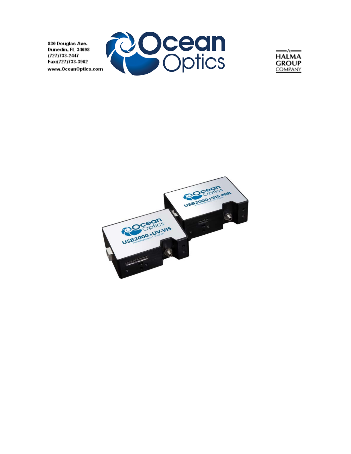
USB2000+ Data Sheet
Description
The Ocean Optics USB2000+ Spectrometer includes the linear CCD-array optical bench, plus all the
circuits necessary for spectrometer operation. The result is a compact, flexible system, with no moving
parts, that's easily integrated as an OEM component.
The USB2000+ spectrometer is a unique combination of technologies providing users with both an
unusually high spectral response and high optical resolution in a single package. The electronics have
been designed for considerable flexibility in connecting to various modules as well as external
interfaces. The USB2000+ interfaces to PCs, PLCs and other embedded controllers through USB 2.0
or RS-232 communications. The information included in this guide provides detailed instructions on
the connection and operation of the USB2000+.
The detector used in the USB2000+ spectrometer is a high-sensitivity 2048-element CCD array from
Sony, product number ILX511. (For complete details on this detector, visit Sony’s web site at
www.sony.com. Ocean Optics applies a coating to all ILX511 detectors, so the optical sensitivity
could vary from that specified in the Sony datasheet).
The USB2000+ operates off of a single +5VDC supply and either a USB or RS-232 interface. The
USB2000+ is a microcontroller-controlled spectrometer, thus all operating parameters are
implemented through software interfacing to the unit.
A special 500 lines/mm groove density grating option used in the USB2000+XR spectrometer
provides broader spectral coverage with no sac ri fice in performance. This extended-range
spectrometer is preconfigured with this new grating for general-purpose UV-NIR applications.
270-00000-000-05-201303 1
Page 2

USB2000+ Data Sheet
Features
• ILX511 Detector
• High sensitivity detector
• Readout Rate: 2.4MHz
• Optics
• An optical resolution of ~0.3nm (FWHM)
• A wide variety of optics available
• 14 gratings, plus Grating #31for the XR version
• 6 slit widths
• 3 detector coatings
• 6 optical filters
• Electrical Performance
• 16 bit, 3MHz A/D Converter
• Integration times from 1ms to 65s
• 5 triggering modes
• Embedded microcontroller allows programmatic control of all operating parameters &
Standalone operation
• USB 2.0 480Mbps (High Speed) & 12Mbps (Full speed)
• RS232 115Kbaud
• Multiple Communication Standards for digital accessories (SPI, I
• Onboard Pulse Generator
• 2 programmable strobe signals for triggering other devices
• Software control of nearly all pulse parameters
• Onboard GPIO
• 8 user programmable digital I/O
• EEPROM storage for
• Wavelength Calibration Coefficients
• Linearity Correction Coefficients
• Absolute Irradiance Calibration (optional)
• Plug-n-Play Interface for PC applications
• 22-pin connector for interfacing to external products
• CE Certification
2
C)
2 270-00000-000-05-201303
Page 3

USB2000+ Data Sheet
Specifications
Specifications Criteria
Absolute Maximum Ratings:
V
CC
Voltage on any pin
Physical Specifications:
Physical Dimensions
Weight
Power:
Power requirement (master)
Supply voltage
Power-up time
Spectrometer:
Design
Focal length (input)
Focal length (output)
Input Fiber Connector
Gratings
Entrance Slit
Detector
Filters
Spectroscopic:
Integration Time
Dynamic Range
Signal-to-Noise
Readout Noise (single dark spectrum)
Resolution (FWHM)
Stray Light
Spectrometer Channels
Environmental Conditions:
Temperature
Humidity
Interfaces:
USB
RS-232
+ 5.5 VDC
Vcc
89.1 mm x 63.3 mm x 34.4 mm
190 g
250 mA at +5 VDC
4.5 – 5.5 V
~2s depending on code size
Asymmetric crossed Czerny-Turner
42mm
68mm (75, 83, and 90mm focal lengths are also available)
SMA 905
14 different gratings, plus Grating #31 for the XR version
5, 10, 25, 50, 100, or 200 μm slits. (Slits are optional. In the
absence of a slit, the fiber acts as the entrance slit.)
Sony ILX511B CCD
nd
2
and 3rd order rejection, long pass (optional)
1 ms – 65 sec
8
2 x 10
(system), 1300:1 (single acquisition)
250:1 single acquisition
50 counts RMS, 300 counts peak-to-peak
0.03 – 10.0 nm varies by configuration (see
www.Oceanoptics.com for configuration options)
<0.05% at 600 nm; <0.10% at 435 nm
One
-30° to +70° C Storage & -10° to +50° C Operation
0% - 90% noncondensing
USB 2.0, 480 Mbps
2-wire RS-232
270-00000-000-05-201303 3
Page 4

USB2000+ Data Sheet
Mechanical Diagrams
Figure 1: USB2000+ Outer Dimensions
4 270-00000-000-05-201303
Page 5
USB2000+ Data Sheet
Pin#
Description
Alt Function
A1
A2
1 VUSB
2
Tx
3
Rx
4
LampEnable
5
ContStrobe
6
GND
7
ExtTrigIn
8 Single Strobe
9 SCL
10
SDA
11
MOSI
12
MISO
13
GPIO-1 (1P)*
14
GPIO-0 (2P)
15
GPIO-3 (1N)
Integration Clock
16
GPIO-2 (2N)
Reserved
17
GPIO-5 (3P)
Acquire Spectra
(Read Enable)
18
GPIO-4 (4P)
Reserved
19
GPIO-7 (3N)
SH CCD pin
20
GPIO-6 (4N)
ICG CCD pin
Pin orientation
20 18 16 14 12 10 8 6 4 2 A2
Electrical Pinout
Listed below is the pin description for the USB2000+ Accessory Connector located on the front
vertical wall of the unit. The connector is a Samtec part # IPT1-111-01-S-D-RA connector. The
vertical mate to this is part #IPS1-111-01-S-D-VS and the right angle PCB mount is part #IPS1-11101-S-D-RA.
SPI_CLK
SPICS_OUT
19 17 15 13 11 9 7 5 3 1 A1
Looking at Front of USB2000+
Master Clock
Base Clock
Notes:
• GPIO nP & nN notation is for future LVDS capability
• 5V Aux pin on the GPIO header is output only
270-00000-000-05-201303 5
Page 6

USB2000+ Data Sheet
Function Input/Output Description
VCC , V
RS232 Tx Output RS232 Transmit signal – for communication with PC connect to
RS232 Rx Input RS232 Receive signal – for communication with PC connect to
Lamp Enable Output A TTL signal that is driven Active HIGH when the Lamp Enable
Continuous
Strobe
Ground Input/Output Ground
Single Strobe Output TTL output pulse used as a strobe signal, which has a
ExtTrigIn Input
or 5Vin Input or Output This is the input power pin to the USB2000+. Additionally when
USB
Output TTL output signal used to pulse a strobe that is divided down from
operating via a Universal Serial Bus (USB) this is the USB power
connection (+5V) which can be used to power other peripherals
(Care must be taken to insure that the peripheral complies with
USB Specifications). NOTE: Do not connect both USB power and
Auxiliary power (as an input) at the same time.
DB9 pin 2
DB9 pin 3.
command is sent to the USB2000+
the Master Clock signal
programmable delay relative to the beginning of the spectrometer
integration period.
The TTL input trigger signal. In External Hardware Trigger mode
this is a rising edge trigger input. In Software Trigger Mode this is
an Active HIGH Level signal. In External Synchronization Mode
(or External hardware Level Trigger Mode) this is a clock input,
which defines the integration period of the spectrometer.
SCL Input/Output
SDA Input/Output
Input/Output 8 2.5V General Purpose Software Programmable Digital
GPIO(0-7)
Output The SPI Master Out Slave In (MOSI) signal for communications to
MOSI
Input The SPI Master In Slave Out (MISO) signal for communications to
MISO
SPI CLK
SPICS_OUT
Output
Output The SPI Chip/Device Select signal for communications to other
The I2C Clock signal for communications to other I2C peripherals
The I2C Data signal for communications to other I2C peripherals
Inputs/Outputs
other SPI peripherals
other SPI peripherals
The SPI Clock signal for communications to other SPI peripherals
SPI peripherals
6 270-00000-000-05-201303
Page 7

USB2000+ Data Sheet
CCD Overview
CCD Detector
The detector used for the USB2000+ is a charge transfer device (CCD) that has a fixed well depth
(capacitor) associated with each photodetector (pixel).
Charge transfer, reset and readout initiation begin with the integration time clock going HIGH. At this
point, the remaining charge in the detector wells is transferred to a shift register for serial transfer. This
process is how the array is read.
The reset function recharges the photodetector wells to their full potential and allows for nearly
continuous integration of the light energy during the integration time, while the data is read out
through serial shift registers. At the end of an integration period, the process is repeated.
When a well is fully depleted by leakage through the back-biased photodetector, the detector is
considered saturated and provides the maximum output level. The CCD is a depletion device and thus
the output signal is inversely proportional to the input photons. The electronics in the USB2000+
invert and amplify this electrical signal.
CCD Well Depth
We strive for a large signal-to-noise (S:N) in optical measurements so that small signal variations can
be observed and a large dynamic range is available. The S:N in photon noise-limited systems is
defined and measured as the square root of the number of photons it takes to fill a well to saturation. In
the USB2000+, the well depth of the CCD pixels is about 160,000 photons, providing a S:N of 400:1
(S:N can also be measured as the saturation voltage divided by near-saturation RMS noise). There is
also a fixed readout noise component to all samples. The result is a system with a S:N of ~275:1.
There are two ways to achieve a large S:N (e.g., 6000:1) in CCD detectors where photon noise is
predominant.
1. Use a large-well device that integrates to saturation over a long period of time until the photon
noise is averaged out by the root of n multiples of a defined short ∆t.
2. Use a small-well device that integrates to saturation at one short ∆t and then signal average
mathematically n times.
Theoretically, both approaches achieve the same results, though there are large differences in actual
operation. Traditional spectroscopic instruments use large-well devices and 16-bit ADCs to achieve
the defined S:N. The USB2000+ uses a small-well device and utilizes signal averaging to achieve the
same S:N. A brief comparison of large and small-well devices is shown in the table below.
270-00000-000-05-201303 7
Page 8

USB2000+ Data Sheet
Well Depth Comparison
Large-well CCDs Small-well CCDs
Low photon noise Medium photon noise that can be averaged out
Low optical sensitivity High optical sensitivity
High power consumption Low power consumption
>10 MHz operating speeds Moderate operating speeds (~2 MHz)
Signal Averaging
Signal averaging is an important tool in the measurement of spectral structures. It increases the S:N
and the amplitude resolution of a set of samples. The types of signal averaging available in our
software are time-based and spatial-based.
When using the time-base type of signal averaging, the S:N increases by the square root of the number
of samples. Signal averaging by summing is used when spectra are fairly stable over the sample
period. Thus, a S:N of 2500:1 is readily achieved by averaging 100 spectra.
Spatial averaging or pixel boxcar averaging can be used to improve S:N when observed spectral
structures are broad. The traditional boxcar algorithm averages n pixel values on each side of a given
pixel.
Time-based and spatial-based algorithms are not correlated, so therefore the improvement in S:N is the
product of the two processes.
In review, large-well devices are far less sensitive than small-well devices and thus, require a longer
integration time for the same output. Large-well devices achieve a good S:N because they integrate out
photon noise. Small-well devices must use mathematical signal averaging to achieve the same results
as large-well devices, but small-well devices can achieve the results in the same period of time. This
kind of signal averaging was not possible in the past because analog-to-digital converters and
computers were too slow.
Large-well devices consume large amoun ts of pow er, resul ting in the need to bui ld therm oelec tric cool ers
to control temperature and redu ce el ect roni c nois e. Then , eve n mor e powe r is requ ire d for th e tem per ature
stabilization hardware. But small-well devices on ly nee d to use s igna l ave ragi ng to ac hiev e the sam e
results as large-well devices, and hav e the adv an tage s of remaining cool and less noisy.
Internal Operation
Pixel Definition
A series of pixels in the beginning of the scan have been covered with an opaque material to
compensate for thermal induced drift of the baseline signal. As the USB2000+ warms up, the baseline
signal will shift slowly downward a few counts depending on the external environment. The baseline
signal is set at the time of manufacture. If the baseline signal is manually adjusted, it should be left
high enough to allow for system drift. The following is a description of all of the pixels, both as they
exist on the hardware device and as they are actually read from the device via USB:
8 270-00000-000-05-201303
Page 9
USB2000+ Data Sheet
Pixels on the Device
Pixel Description
0–11 Not usable
12–29 Optical black pixels
30–31 Not usable
32–2079 Optical active pixels
2080–2085 Not usable
Pixels Read from the Device via USB
Pixel Description
0–17 Optical black pixels
18–19 Not usable
20-2047 Optical active pixels
It is important to note that the USB2000+ only digitizes the first 2048 pixels.
CCD Detector Reset Operation
At the start of each integration period, the detector transfers the signal from each pixel to the readout
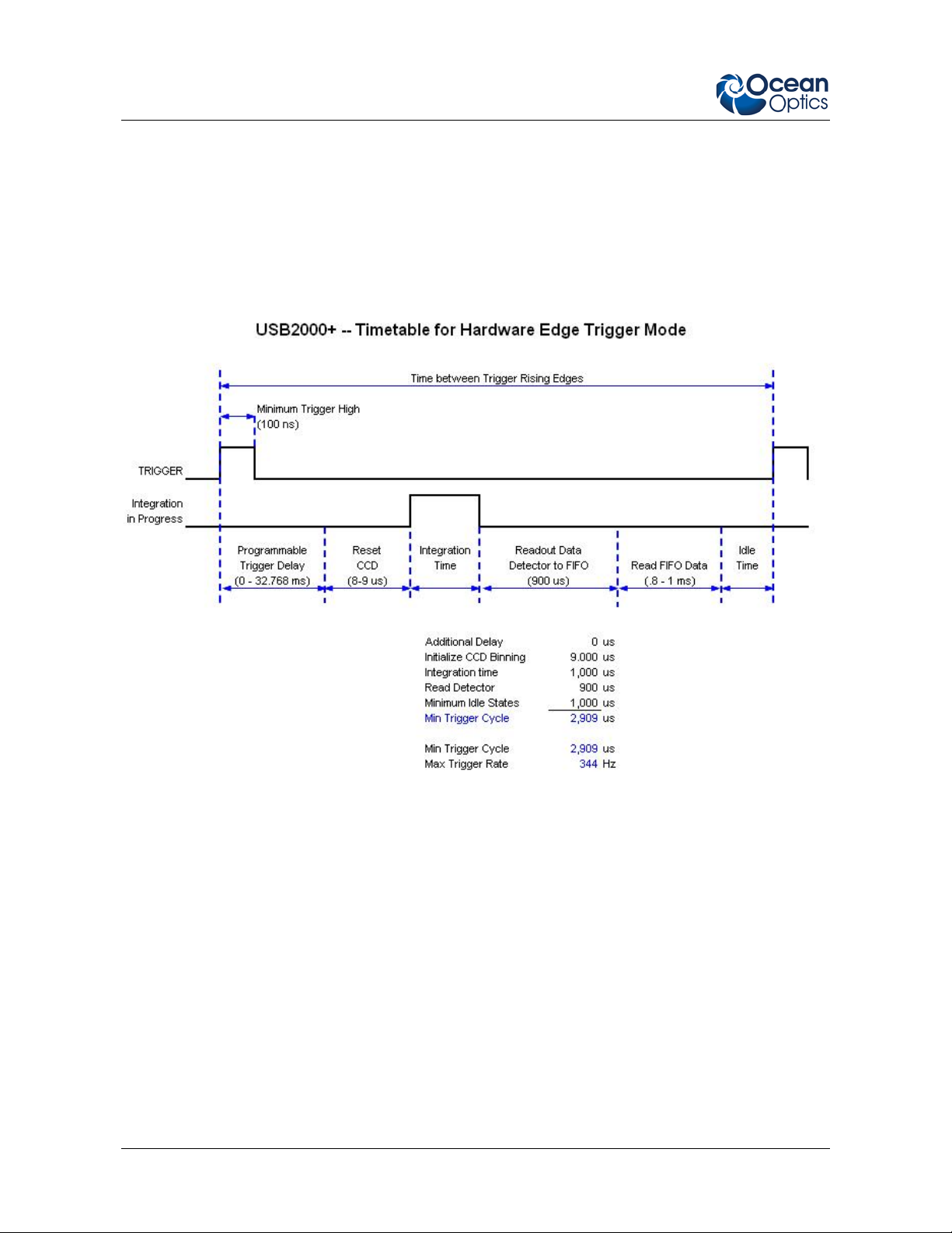
registers and resets the pixels. The total amount of time required to perform this operation is ~8 − 9µs.
The user needs to account for this time delay when the pixels are optically inactive, especially in the
external triggering modes.
Timing Signals
Strobe Signals
Single Strobe
The Single Strobe signal is a programmable TTL pulse that occurs at a user-determined time during
each integration period. This pulse has a user-defined High Transition Delay and Low Transition
Delay. The pulse width of the Single Strobe is the difference between these delays. It is only active if
the Lamp Enable command is active.
Synchronization of external devices to the spectrometer's integration period is accomplished with this
pulse. The Strobe Delay is specified by the Single Strobe High Transition Delay (SSHTD) and the
Pulse Width is specified by the Single Strobe Low Transition Delay (SSLTD) minus the Single Strobe
High Transition Delay ( PW = SSLTD – SSHTD). Both values are programmable in 500ns
increments for the range of 0 to 65,535 (32.7675ms).
270-00000-000-05-201303 9
Page 10
USB2000+ Data Sheet
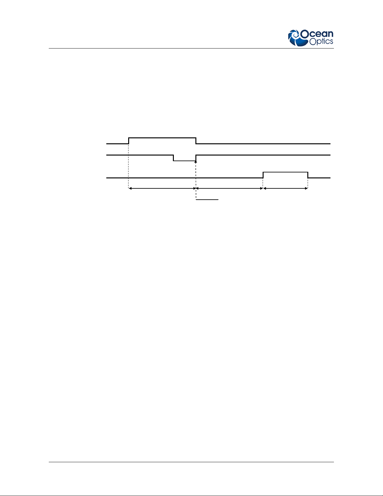
External Trigger Input
φROG
Single Strobe
t_SOID+TD t_SSHTD
SOI
t_SOID Start Of Integration Delay (8.2 - 8.5us)
t_TD Trigger Delay
t_SSHTD Single Strobe High Transition Del ay
t_SSLTD Single Strobe Low Transition Delay
t_SSLTD
The timing of the Single Strobe is based on the Start of Integration (SOI). SOI occurs on the rising
edge of φROG which is used to reset the Sony ILX511 detector. In all trigger modes using an External
Trigger, there is a fixed relationship between the trigger and the SOI. In the Normal mode and
Software Trigg er m ode, the SOI still marks the beginning of the Single Strobe, but due to the
nondeterministic timing of the software and computer operating system, this timing will change over
time and is not periodic. That is, at a constant integration time, the Single Strobe will not be periodic,
but it will indicate the start of the integration. The timing diagram for the Single Strobe in External
Hardware Trigger mode is shown below:
Single Strobe (External Hardware Trigger/External Synchronous Trigger Mode)
The Trigger Delay (TD) is another user programmable delay which specifies the time in 500ns
increments that the SOI will be delayed beyond the normal Start of Integration Delay (SOID).
An example calculation of the Single Strobe timing follows:
If the TD = 1ms, SSHTD = 50ms, and SSLTD = 70ms then, the rising edge of the Single Strobe will
occur approximately 51.82ms (1ms + 50ms + 8.2us) after the External Trigger Input goes high and the
Pulse Width will be 20ms (70ms – 50ms).
Continuous Strobe
The Continuous Strobe signal is a programmable frequency pulse-train with a 50% duty cycle. It is
programmed by specifying the desired period whose range is 2us to 60s. This signal is continuous
once enabled, but is not synchronized to the Start of Integration or External Trigger Input. The
Continuous Strobe is only active if the Lamp Enable command is active.
Synchronizin g St r obe Events
If the application requires more than one pulse per integration period, the user needs to insure the
continuous strobe and integration period are synchronized. The integration time must be set so that an
equal number of strobe events occurs during any given integration period.
10 270-00000-000-05-201303
Page 11

USB2000+ Data Sheet
Triggering Modes
The USB2000+ supports four triggering modes, (plus Normal mode), which are set with the Trigger
Mode command. Detailed information of each triggering mode follows. Also refer to the External
Triggering Options document for Firmware versions 3.0 and above located on our website at
http://www.oceanoptics.com/technical/External-Triggering2.pdf
describe these modes. For firmware version below 3.0, see
http://www.oceanoptics.com/technical/External-Triggering.pdf.
Normal
In the Normal (Free-run) mode, the spectrometer will acquire a spectrum based on the integration
period specified through the software interface. This data is made available for reading as soon as all
the data is stored. The spectrometer will then immed iately try to acquire two additional spectra even if
none have been requested. If a new spectrum request has come from the user, during either the second
or third integration cycle then the appropriate spectrum will be availab le to the use r. If a second
spectrum has not been requested then the Spectrometer will not save the second or third spectrum and
will go into an idle mode waiting for a new spectrum request from the user. In this scenario, a new
acquisition begins when a new spectrum is requested. No further spectra are acquired until the original
spectrum is read by the user.
Software Trigger Mode
. The following paragraphs
In this level-triggered mode, the spectrometer is “free running,” just as it is in the Normal mode. The
spectrometer is continually scanning and collecting data. With each trigger, the data collected up to the
trigger event is transferred to the software. If you continuously apply triggers (for example, by holding
down the button on via an external switch), this mode is equivalent to operating in the Normal mode.
In the Software Trigger mode, you set the integration time (as well as all other acquisition parameters)
in the software. The source for the integration clock comes from the A/D converter.
External Synchronous Trigger Mode
In the External Synchronous Trigger mode, two external triggers are required to complete a data
acquisition. The first rising edge starts the integration period and the second rising edge stops the
integration and starts the next. Thus the integration time is the period between the two external trigger
pulses. After the integration period, the spectrum is retrieved and available to the user. As in normal
mode, no further spectra are acquired until the original spectrum is read by the user.
External Hardware Level Trigger Mode
In the External Hardware Level Trigger mode, a rising edge detected by the spectrometer from the
External Trigger input starts the integra tion per iod spe cified th rough the software interface. After the
integration period, the spectrum is retrieved and is ready to be read by the user. As long as the trigger
level remains active in a logic one state, back-to-back acquisitions can occur, as in the Normal mode,
until the trigger transitions to an inactive level. As in normal mode, no further spectra are acquired
until the original spectrum is read by the user.
270-00000-000-05-201303 11
Page 12
USB2000+ Data Sheet
External Hardware Edge Trigger Mode
In the External Hardware Edge Trigger mode, a rising edge detected by the spectrometer from the
External Trigger input starts the integ ra tion period spe cified th roug h the softwar e interf ace. After the
integration period, the spectrum is retrieved and is ready to be read by the user. If another trigger is
sent a new integration cycle will begin. If a spectrum request is not received before the integration
cycle has ended then that data will be deleted and a new trigger and spectrum request is required.
Only one acquisition will be performed for each External Trigger pulse, no matter what the pulse’s
duration is. No further spectra are acquired unti l the original spectrum is read by the user.
Digital Inputs & Outputs
General Purpose Inputs/Outputs (GPIO)
The USB2000+ has 8 user programmable 2.5V TTL digital Input/Output pins, which can be accessed
at the 22-pin accessory connector. Through software, the state of these I/O pins can be defined and
used for multi-purpose applications such as communications buses, sending digital values to an
LCD/LED display, or even implementing complex feedback systems.
GPIO Recommended Operating Levels:
VIL(max) = 0.7V
VIH(min) = 1.7V
12 270-00000-000-05-201303
Page 13

USB2000+ Data Sheet
IOL = 24mA
IOH = -24mA
GPIO Absolute Maximum Ratings are as follows:
VIN(min) = -0.5V
VIN(max) = 3.0V
Communication and Interface
USB 2.0
480-Mbit Universal Serial Bus allows for ultra fa st data trans fer . This is the main communication
standard for PC users. The USB BUS also provides power as well as communications over a single
cord. Thereby allowing the USB2000+ to operate anywhere you can take a laptop computer without
any bulky external power supplies.
RS-232
Also known as serial port communication, RS232 is a standard in PC and industrial device
communications. Using transmit and receive signals this option allows the USB2000+ to be a
standalone device, which can output data to other logic devices/controllers such as a PLC or
microcontroller. The USB2000+ requires an external 5-Volt power source when operating in RS-232
mode.
I2C
Inter-Integrated Circuit 2-Wire serial BUS is widely used in embedded systems applications. With I²C
you can add peripherals to your system without using valuable resources like I/O ports.
SPI
Serial Peripheral Interface is also a widely used communication standard in embedded systems
applications. It is a 3-wire interface that can be used to communicate to multiple slave devices.
270-00000-000-05-201303 13
Page 14

USB2000+ Data Sheet
USB2000+ USB Port Interface Communications and Control Information
Overview
The USB2000+ is a microcontroller-based Miniature Fiber Optic Spectrometer that can communicate
via the Universal Serial Bus or RS-232. This section contains the necessary command information for
controlling the USB200 via the USB interface. This information is only pertinent to users who wish to
not utilize Ocean Optics 32 bit driver to interface to the USB2000+. Only experienced USB
programmers should attempt to interface to the USB2000+ via these methods.
Hardware Description
The USB2000+ utilizes a Cypress CY7C68013 microcontroller that has a high speed 8051 combined
with an USB2.0 ASIC. Program code and data coefficients are stored in external E
loaded at boot-up via the I
SRAM. Maximum throughput for spectral data is achieved when data flows directly from the external
FIFO’s directly across the USB bus. In this mode the 8051 does not have access to the data and thus
no manipulation of the data is possible.
2
C bus. The microcontroller has 16K of internal SRAM and 64K of external
2
PROM that are
USB Information
Ocean Optics Vendor ID number is 0x2457 and the Product ID is 0x101E.
Instruction Set
Command Syntax
The list of the commands is shown in the following table followed by a detailed description of each
command. The length of the data depends on the command. All commands are sent to the USB2000+
through End Point 1 Out (EP1). All spectra data is acquired through End Point 2 In and all other
queries are retrieved through End Point 1 In (EP1). The endpoints enabled and their order is:
Pipe # Description Type
Hi Speed Size
(Bytes)
Full Speed
Size (Bytes)
Endpoint
Address
0 End Point 1 Out Bulk 64 0x01
1 End Point 2 In Bulk 512 0x82
2 End Point 6 In Bulk 512 0x86
3 End Point 1 In Bulk 64 0x81
14 270-00000-000-05-201303
Page 15

USB2000+ Data Sheet
USB Command Summary
EP1
Command
Description
Version
Byte Value
0x01 Initialize USB2000+ 0.90.0
0x02 Set Integration Time 0.90.0
0x03 Set Strobe Enable Status 0.90.0
0x04 Set Shutdown Mode 0.90.0
0x05 Query Information 0.90.0
0x06 Write Information 0.90.0
0x09 Request Spectra 0.90.0
0x0A Set Trigger Mode 0.90.0
0x0B Query number of Plug-in Accessories Present 0.90.0
0x0C Query Plug-in Identifiers 0.90.0
0x0D Detect Plug-ins 0.90.0
0x60 General I2C Read 0.90.0
0x61 General I2C Write 0.90.0
0x62 General SPI I/O 0.90.0
0x6A Write Register Information 0.90.0
0x6B Read Register Information 0.90.0
0x6C Read PCB Temperature 0.90.0
0x6D Read Irradiance Calibration Factors 0.90.0
0x6E Write Irradiance Calibration Factors 0.90.0
0xFE Query Information 0.90.0
USB Command Descriptions
A detailed description of all USB2000+ commands follows. While all commands are sent to EP1 over
the USB port, the byte sequence is command dependent. The general format is the first byte is the
command value and the additional bytes are command specific values.
Byte 0 Byte 1 Byte 2 … Byte n-1
Command
Byte
Command
Specific
Command
Specific
… Command
Specific
270-00000-000-05-201303 15
Page 16

USB2000+ Data Sheet
Data Byte = 0 Lamp Enable Low/Off
Initialize USB2000+
Initializes certain parameters on the USB2000+ and sets internal variables based on the USB
communication speed the device is operating at. This command should be called at the start of every
session however if the user does not call it, it will be executed on the first Request Scan command.
The default values are set as follows:
Parameter Default Value
Trigger Mode 0 – Normal Trigger
Byte Format
Byte 0
0x01
Set Integration Time
Sets the USB2000+ integration time in microseconds. The value is a 32-bit value whose acceptable
range is 1,000µs – 65,535,000µs. If the value is outside this range the value is unchanged. For
integration times less than 655,000us, the integration counter has a resolution of 10us. For integration
times greater than this the integration coun te r has a resolut ion of 1m s.
Byte Format
Byte 0 Byte 1 Byte 2 Byte 3 Byte 4
0x02
LSWLSB
LSW-MSB MSW-LSB MSW-MSB
MSW & LSW: Most/Least Significant Word
MSB & LSB: Most/Least Significant Byte
Set Strobe Enable Status
Sets the USB2000+ Lamp Enable line (J2 pin 4) as follows. The Single Strobe and Continuous Strobe
signals are enabled/disabled by this Lamp Enable Signal.
Data Byte = 1 Lamp Enable HIGH/On
Byte Format
Byte 0 Byte 1 Byte 2
0x03 Data byte LSB Data Byte MSB
16 270-00000-000-05-201303
Page 17

USB2000+ Data Sheet
Data Byte = 0 Shutdown everything but the FX2
Set Shutdown Mode
Sets the USB2000+ shutdown mode. When shutdown, the internal FX2 microcontroller is
continuously running however all other functionality is disabled. In this power down mode the current
consumption is reduced to 250mA (operating current for the FX2 microcontroller). When shutdown is
active (active low), the external 5V signal (V5_Switched pin 3) is disabled in addition to all other
signals except I
2
C lines.
Data Byte = !0 Power up entire Spectrometer
Byte Format
Byte 0 Byte 1 Byte 2
0x04 Data byte LSB Data Byte MSB
Query Information
Queries any of the 20 stored spectrometer configuration variables. The Query command is sent to End
Point 1 Out and the data is retrieved through End Point 1 In. When using Query Information to read
EEPROM slots, data is returned as ASCII text. However, everything after the first byte that is equal to
numerical zero will be returned as garbage and should be ignored.
The 20 configuration variables are indexed as follows:
270-00000-000-05-201303 17
Page 18

USB2000+ Data Sheet
Configuration Idex - Description
0 – Serial Number
th
order Wavelength Calibration Coefficient
1 – 0
st
order Wavelength Calibration Coefficient
2 – 1
nd
order Wavelength Calibration Coefficient
3 – 2
rd
order Wavelength Calibration Coefficient
4 – 3
5 – Stray light constant
th
order non-linearity correction coefficient
6 – 0
st
order non-linearity correction coefficient
7 – 1
nd
order non-linearity correction coefficient
8 – 2
rd
order non-linearity correction coefficient
9 – 3
th
10 – 4
11 – 5
12 – 6
13 – 7
order non-linearity correction coefficient
th
order non-linearity correction coefficient
th
order non-linearity correction coefficient
th
order non-linearity correction coefficient
14 – Polynomial order of non-linearity calibration
15 – Optical bench configuration: gg fff sss
gg – Grating #, fff – filter wavelength, sss – slit size
16 – USB2000+ configuration: AWL V
A – Array coating Mfg, W – Array wavelength (VIS, UV, OFLV), L – L2 lens
installed, V – CPLD Version
17 – Reserved
18 – Reserved
19 – Reserved
Byte Format
Byte 0 Byte 1
0x05
Configuration
Index
Return Format (EP1)
The data is returned in ASCII format and read in by the host through End Point 1.
Byte 0 Byte 1 Byte 2 Byte 3 … Byte 16
0x05 Configuration Index ASCII byte 0 ASCII byte 1 … ASCII byte 14
Write Informatio n
Writes any of the 19 stored spectrometer configuration variables to EEPROM. The 19 configuration
variables are indexed as described in the Query Information. The information to be written is
transferred as ASCII information.
Byte Format
Byte 0 Byte 1 Byte 2 Byte 3 … Byte 16
18 270-00000-000-05-201303
Page 19

USB2000+ Data Sheet
0x06 Configuration Index ASCII byte 0 ASCII byte 1 … ASCII byte 14
Request Spectra
Initiates sp ectra acqu is it ion. The USB2000+ will acquire a complete spectr um (2048 pixel values).
The data is returned in bulk transfer mode through EP2. The table below provides the pixel order
overview for the 2 different speeds. The pixel values are decoded as described below.
Byte Format
Byte 0
0x09
Return Format
The format for the returned spectral data is dependant upon the USB communication speed.
The format for both High Speed (480 Mbps) and Full Speed (12Mbps) is shown below. All
pixel values are 16 bit values which are organized in LSB | MSB order. There is an additional
packet containing one value that is used as a flag to insure proper synchronization between the
PC and USB2000+.
USB High Speed (480Mbps) Packet Format
The data is read from EP2In. The packet format is described below.
Packet # End Point # Bytes Pixels
0 EP2In 512 0-255
1 EP2In 512 256-511
2 EP2In 512 512-767
3 EP2In 512 768-1023
4 EP2In 512 1024-1279
5 EP2In 512 1280-1535
… EP2In 512
8 EP2In 512 1792–2048
9 EP2In 1 Sync Packet
The format for the first packet is as follows (all other packets except the synch packet has a
similar format except the pixel numbers are incremented by 256 pixels for each packet).
Packet 0
Byte 0 Byte 1 Byte 2 Byte 3
Pixel 0 LSB Pixel 0 MSB Pixel 1 LSB Pixel 1 MSB
…
Byte 510 Byte 511
270-00000-000-05-201303 19
Page 20

USB2000+ Data Sheet
Pixel 255 LSB Pixel 255 MSB
Packet 15 – Synchronization Packet (1 byte)
Byte 0
0x69
USB Full Speed (12Mbps) Packet Format
In this mode all data is read from EP2In. The pixel and packet format is shown below.
Packet # End Point # Bytes Pixels
0 EP2In 64 0-31
1 EP2In 64 32-63
2 EP2In 64 64-95
… EP2In 64
63 EP2In 64 2016-2047
64 EP2In 1 Sync Packet
Packet 0
Byte 0 Byte 1 Byte 2 Byte 3
Pixel 0 LSB Pixel 0 MSB Pixel 1 LSB Pixel 2 MSB
…
Byte 62 Byte 63
Pixel 31 LSB Pixel 31 MSB
Packet 64 – Synchronization Packet (1 byte)
Byte 0
0x69
Autonulling
Slot 0x11 (17) contains autonulling information that has a scaling term used to adjust the magnitude of
the entire spectrum. This can be read out by send ing bytes 0x05 11 to the low-speed out endpoint
(0x01) and then reading out 17 bytes from the low-speed in endpoint (0x81). The bytes of use are
Byte offset 6 and 7. The 17 bytes will be formatted as follows:
0x05 11 XX XX XX XX S S SS XX XX XX X X XX XX XX XX XX
Where:
XX = reserved bytes (most are either unused or are only used internally to the device)
20 270-00000-000-05-201303
Page 21

USB2000+ Data Sheet
SS = saturation level of the device as two bytes (LSB followed by MSB).
These need to be assembled into a single 16-bit value. Any time that a spectrum is read from the
spectrometer, each pixel’s intensity value should be multiplied by (65535.0/saturation_level) to set the
scale appropriately.
The contents of slot 0x11 are set at the factory and should not be altered.
Set Trigger Mode
Sets the USB2000+ Trigger mode to one of five states. If an unacceptable value is passed then the
trigger state is unchanged (refer to the External Triggering Options Instructions
for a description of the
trigger modes).
Data Value = 0 Normal (Free running) Mode
Data Value = 1 Software Trigger Mode
Data Value = 2 External Hardware Level Trigger Mode
Data Value = 3 External Synchron izati on Tr igger Mo de
Data Value = 4
External Hardware Edge Trigger Mode
Byte Format
Byte 0 Byte 1 Byte 2
0x0A Data Value LSB Data Value MSB
Query Number of Plug-in Accessories
To query the number of preset plug-in accessories, use the Query Plug-in Identifiers command 0x0C
(below), matching plug-in IDs to the known IDs.
Query Plug-in Identifiers
Queries the Plug-in accessories identifiers. This command returns 7 bytes with the last byte always
being zero at this point. Each of the first 6 bytes correspond to Ocean Optics compatible devices which
responded appropriately for I
various categories of devices and the value for each category is shown below. I
2
C addresses 2 through 7 respectively. The I2C addresses are reserved for
2
C addresses 0-1 are
reserved for loading program code from EEPROMS
Byte Format
Byte 0
0x0C
Return Format
The data is returned in Binary format and read in by the host through End Point 7.
Byte 0 Byte 1 … Byte 5 Byte 6
Value @ I2C address 2 Value @ I2C address 3 … Value @ I2C address 7 0x00
270-00000-000-05-201303 21
Page 22

USB2000+ Data Sheet
Detect Plug-ins
Reads all of the plug-in accessories that are plugged into the I2C bus. No data values are returned.
Byte Format
Byte 0
0x0D
General I2C Read
Performs a general purpose read on the I2C pins for interfacing to attached peripherals. The time to
complete the command is determined by the amount of data transferred and the response time of the
peripheral. The I
2
C bus runs at 400KHz. The maximum number of bytes that can be read is 61.
Command Byte Format
Byte 0 Byte 1 Byte 2
0x60 I2C Address Bytes to Read
Return Byte Format
Byte 0 Byte 1 Byte 2 Byte 3 … Byte N+3
I2C Results I2C Address Bytes to Read Data Byte 0 … Data byte N
I2C Result Value Description
0 I2C bus Idle
1 I2C bus Sending Data
2 I2C bus Receiving Data
3 I2C bus Receiving first byte of string
5 I2C bus in waiting for STOP condition
6 I2C experienced Bit Error
7 I2C experience a Not Acknowledge (NAK) Condition
8 I2C experienced successful transfer
9 I2C bus timed out
General I2C Write
Performs a general purpose write on the I2C pins for interfacing to attached peripherals. The time to
complete the command is determined by the amount of data transferred and the response time of the
peripheral. In all I2C communications, the first byte of the transaction consists of a 7 bit address and a
read/write bit. The “address” that is passed as the second byte of the I2C write command is this 7 bit
address, which will be shifted 1 bit left and appended with the R/W bit to form the first byte of the I2C
write transaction. The I
22 270-00000-000-05-201303
2
C bus runs at 400KHz. The results codes are described above.
Page 23

USB2000+ Data Sheet
Command Byte Format
Byte 0 Byte 1 Byte 2 Byte 3 … Byte N+3
0x61
2
C Address
I
Bytes to
Write
Data Byte 0 … Data byte N
Return Byte Format
Byte 0
I2C Results
General SPI Input/Output
Performs a general-purpose write and read on the SPI bus for interfacing to attached peripherals. The
time to complete the command is determined by the amount of data transferred and the response time
of the peripheral. Wait at least 10 ms after sending a Write command before reading the Return value.
The SPI bus runs at ~125KHz Clock. The maximum number of bytes that can be written or read is 61.
During this transfer the SPI Chip Select signal is driven to an active LOW TTL level. Data is
transmitted out the MOSI (Master Out Slave In) line on the rising edge of the clock signal. Data is also
latched in the from the MISO line on the falling edge of the clock signal.
Command Byte Format
Byte 0 Byte 1 Byte 2 Byte 3 … Byte N+2
0x62
# of Bytes (N) Write Byte 0 Write Byte 1 … Write Byte
N
Return Byte Format
Byte 0 Byte 1 Byte 2 … Byte N+1
# of Bytes (N) Read Byte 0 Read Byte 1 … Read Byte N
Write Register Information
Most all of the controllable parameters for the USB2000+ are accessible through this command (e.g.,
GPIO, strobe parameters, etc). A complete list of these parameters with the associate register
information is shown in the table below. Commands are written to End Point 1 Out typically with 4
bytes (some commands may require more data bytes). All data values are 16 bit values transferred in
LSB | MSB order. This command requires 100us to complete; the calling program needs to delay for
this length of time before issuing another command. In some instances, other commands will also
write to these registers (i.e., int eg ra t ion time), in these cases the user has the options of setting the
parameters through 2 different methods.
Byte Format
Byte 0 Byte 1 Byte 2 Byte 3
0x6A
Register
Value
Data Byte LSB Data Byte
MSB
270-00000-000-05-201303 23
Page 24

USB2000+ Data Sheet
Register
Description
Default
Value
Min
Value
Max
Value
Time Base
Version
Address
0x00* Master Clock Counter Divisor 24 1 0xFFFF 48MHz 1.00.0
0x04
0x08
0x0C
0x0C
0x10*
0x10* Integration Period LSB Register 480 0 0xFFFF 1KHz 3.00.0
0x14
FPGA Firmware Version (Read
Only)
Continuous Strobe Timer
Interval Divisor
Continuous Strobe Base Clock
Divisor
Continuous Strobe LSB
Register
Integration Period Base Clock
Divisor
Set base_clk or base_clkx2
0: base_clk
1: base_clkx2
1.00.0
Continuous Strobe
48000 0 0xFFFF
4800 0 0xFFFF 48MHz 1.00.0
4800 0 0xFFFF 48MHz 3.00.0
480 0 0xFFFF 48MHz 1.00.0
0 0 1 N/A 1.00.0
Base Clock
(see Register
0x0C)
1.00.0
Integration Period
0x18* Integration Clock Timer Divisor 600 0 0xFFFF
0x18*
0x20 Reserved 1.00.0
0x28
0x28
0x2C&*
Integration Period MSB
Register
Hardware Trigger Delay –
Number of Master Clock cycles
to delay when in External
Hardware Trigger mode before
the start of the integration
period
Hardware Trigger Delay –
Delay the start of integration
from the rising edge of the
trigger in 500ns increments
Trigger Mode
0 = Free Running
1 = Software Trigger
2 = External Hardware Trigger
3 = External Synchronization
Trigger
3.00.0
0 0 0xFFFF 1.00.0
0 0 0xFFFF 3.00.0
0 0 3 1.00.0
Base Clock
(see Register 0x10)
1.00.0
24 270-00000-000-05-201303
Page 25

USB2000+ Data Sheet
Register
Description
Default
Value
Min
Value
Max
Value
Time Base
Version
Address
Trigger Mode
0 = Free Running
1 = Software Trigger
2 = External Hardware Level
0x2C&*
0x30 Reserved 1.00.0
0x38
0x3C
0x40 Lamp Enable 0 0 1 N/A 1.00.0
0x48
Trigger
3 = External Synchronization
Trigger
4 = External Hardware Edge
Trigger
Single Strobe High Clock
Transition Delay Count
Single Strobe Low Clock
Transition Delay Count
GPIO Mux Register
0: pin is GPIO pin
1: pin is alternate function
0 0 4 N/A 3.00.0
1 0 0xFFFF 2MHz 1.00.0
5 0 0xFFFF 2MHz 1.00.0
0 0 0x03FF N/A 1.00.0
GPIO Output Enable
0x50
0x54
0x58 Reserved 1.00.0
0x5C Offset Value 0 0 0xFFFF N/A 1.00.0
0x60
0x64
0x68 Maximum Saturation Level 0x55F0 0 0xFFFF N/A 1.00.0
1: pin is output
0: pin is input
GPIO Data Register
For Ouput: Write value of
signal
For Input: Read current GPIO
state
Offset Control
Bit 0 = Enable Auto-Nulling
Bit 1 = Enable Auto-Nulling
Saturation
FPGA Programmed (Read
Only)
Notes: * - User should not change these values because spectrometer performance can be affected.
This information is included just for completeness
& - These values are controlled by other command interfaces to the USB2000+ (i.e., Set
integration time command).
0 0 0x03FF N/A 1.00.0
0 0 0x03FF N/A 1.00.0
0 0 0xFFFF N/A 1.00.0
0x5501 N/A N/A N/A 1.00.0
270-00000-000-05-201303 25
Page 26

USB2000+ Data Sheet
Read Register Information
Read the values from any of the registers above. This command is sent to End Point 1 Out and the data
is retrieved through End Point 1 In.
Byte Format
Byte 0 Byte 1
0x6B
Register
Value
Return Format (EP1In)
Byte 0 Byte 1 Byte 2
Register Value Value LSB Value MSB
Read PCB Temperature
Read the Printed Circuit Board Temperature. The USB2000+ contains an DS1721 temperature sensor
chip which is mounted to the under side of the PCB. This command is sent to End Point 1 Out and the
data is retrieved through End Point 1 In. The value returned is a signed 16-bit A/D conversion value,
which is equated to temperature by:
Temperature (
o
C) = .003906 * ADC Value
Byte Format
Byte 0
0x6C
Return Format (EP1In)
Byte 0 Byte 1 Byte 2
Read Result ADC Value LSB ADC Value MSB
If the operation was successful, the Read Result byte value will be 0x08. All other values indicate the
operation was unsuccessful .
Read Irradiance Factors
Reads 60 bytes of data, which is utilized for Irradiance Calibration information from the desired
EEPROM memory address.
Byte Format
Byte 0 Byte 1 Byte 2
0x6D EEPROM Address LSB EEPROM Address MSB
26 270-00000-000-05-201303
Page 27

USB2000+ Data Sheet
Return Byte Format
Byte 0 Byte 1 … Byte 59
Byte 0 Byte 1 … Byte 59
Write Irradiance Factors
Write 60 bytes of data, which is utilized for Irradiance Calibration information to the desired
EEPROM memory address.
Byte Format
Byte 0 Byte 1 Byte 2 Byte 3 … Byte 62
0x6E EEPROM Address LSB EEPROM Address MSB Byte 0 … Byte 59
Query Status
Returns a packet of information containing the current operating information. Packet structure is given
below:
Byte Format
Byte 0
0xFE
Return Format
The data is returned in Binary format and read in by the host through End Point 1 In. The
structure for the return information is as follows:
Byte Description Comments
0-1
2-5
6
7 Trigger Mode Value
8 Spectral Acquisition Status
9
10
11 Packet Count Number of packets loaded into End Point Memory
12 Reserved
Number of Pixels - WORD LSB | MSB order
Integration Time - WORD
Lamp Enable 0 – Signal LOW
Packets In Spectra Returns the number of Packets in a Request Spectra
Power Down Flag 0 – Circuit is powered down
Integration time in µs – LSW | MSW. Within each word
order is LSB | MSB
1 – Signal HIGH
Command.
1 – Circuit is powered up
13 Reserved
14
15 Reserved
270-00000-000-05-201303 27
USB Communications
Speed
0 – Full Speed (12Mbs)
0x80 – High Speed (480 Mbps)
Page 28

USB2000+ Data Sheet
Appendix A: USB2000+ Serial Port Interface Communications and Control Inform ati on
Overview
The USB2000+ is a microcontroller-based Miniature Fiber Optic, which can communicate via the
Universal Serial Bus or RS-232. This document contains the necessary command information for
controlling the USB2000+ via the RS-232 interface.
Hardware Description
Overview
The USB2000+ utilizes a Cypress FX2 microcontroller, which has a high speed 8051, combined with
an USB ASIC. Program code and data coefficients are stored in external E
at boot-up via the I
2
C bus.
2
PROM, which are loaded
Instruction Set
Command Syntax
The list of the commands are shown in the following table along with the microcode version number
they were introduced with. All commands consist of an ASCII character passed over the serial port,
followed by some data. The length of the data depends on the command. The format for the data is
either ASCII or binary (default). The ASCII mode is set with the “a” command and the binary mode
with the “b” command. To insure accurate communications, all commands respond with an ACK
(ASCII 6) for an acceptable command or a NAK (ASCII 21) for an unacceptable command (i.e. data
value specified out of range).
28 270-00000-000-05-201303
Page 29

USB2000+ Data Sheet
In the ASCII data value mode, the USB2000+ “echoes” the command back out the RS-232 port. In
binary mode all data, except where noted, passes as 16-bit unsigned integers (WORDs) with the MSB
followed by the LSB. By issuing the “v command” (Version number query), the data mode can be
determined by viewing the response (ASCII or binary).
In a typical data acquisition session, the user sends commands to implement the desired spectral
acquisition parameters (integration time, etc.). Then the user sends commands to acquire spectra (S
command) with the previously set parameters. If necessary, the baud rate can be changed at the
beginning of this sequence to speed up the data transmission process.
Upgrading from USB2000
Below are a summary of the changes that may be required if you are upgrading from a USB2000 to
USB2000+
• Baud rates
• The startup baud rate is programmable through the EEPROM Calibration Entry #18
• The unit operates at 115.2K Baud, but does not run at 57.6K Baud
• Operating Parameters
• The I (upper case) command will set the integration time in milliseconds
• To take advantage of the microsecond integration time capability, use the i (lower case)
command
• Most new operating parameters are set through the FPGA (W command)
• Spectral Data
• If only one spectra is “Accumulated”, then data is returned in 16 bit format
• If additional spectra is “Accumulated”, then data is returned in 32 bit format
• The limitation of “Accumulating” 15 spectra is eliminated
RS232 Command Summary
Letter Description Version
A Adds scans 1.00.0
B Set Pixel Boxcar 1.00.0
C
D
E
F ***Non functional but follows SAD500 command format***
G Set Data Compression 1.00.0
H ***Non functional but follows SAD500 command format***
I Sets integration time 1.00.0
J Sets Lamp Enable Line 1.00.0
K Changes baud rate 1.00.0
270-00000-000-05-201303 29
Page 30

USB2000+ Data Sheet
Letter Description Version
L Clear Memory
M Set Data Storage Mode 1.00.0
N
O
P Partial Pixel Mode 1.00.0
Q
R
S Starts spectral acquisition with previously set parameters 1.00.0
T Sets trigger mode 1.00.0
U
V
W Query scans in memory 1.00.0
X
Y
Z Read out Scan from memory 1.00.0
A Set ASCII mode for data values 1.00.0
b Set binary mode for data values 1.00.0
k Sets Checksum mode 1.00.0
o Oxygen (USB-LS-450) related commands 1.00.0
t
u Set Oxygen Calibration Coefficients 1.00.0
v Provides microcode version # 1.00.0
x Sets calibration coefficients 1.00.0
y Sets 16-bit timer operation 1.00.0
? Queries parameter values 1.00.0
+ Reads the plugged-in accessories 1.00.0
_ USB2000 Identifier 1.00.0
Command Descriptions
A detailed description of all USB2000+ commands follows. The {} indicates a data value which is
interpreted as either ASCII or binary (default). The default value indicates the value of the parameter
upon power up.
30 270-00000-000-05-201303
Page 31
USB2000+ Data Sheet
Add Scans
Sets the number of discrete spectra to be summed together. Since the USB2000+ has the ability to
return 32 bit values, overflow of the raw 16 bit ADC value is not a concern.
Command Syntax: A{DATA WORD}
Response: ACK or NAK
Range: 1-5000
Default value: 1
Pixel Boxcar Width
Sets the number of pixels to be averaged together. A value of n specifies the averaging of n pixels to
the right and n pixels to the left. This routine uses 32-bit integers so that intermediate overflow will
not occur; however, the result is truncated to a 16-bit integer prior to transmission of the data. This
math is performed just prior to each pixel value being transmitted out. Values greater than ~3 will
exceed the idle time between values and slow down the overall transfer process.
Command Syntax: B{DATA WORD}
Response: ACK or NAK
Range: 0-15
Default value: 0
Set Data Compression
Specifies whether the data transmitted from the USB2000+ should be compressed to speed data
transfer rates.
Command Syntax: G{DATA WORD}
Response: ACK or NAK
Range:
Default value: 0
0 – Compression off
!0 – Compression on
Integration Time (16 bit)
Sets the USB2000+’s integration time, in milliseconds, to the value specified. This command is the
same as on the USB2000.
Command Syntax: I{16 bit DATA WORD}
Response: ACK or NAK
Range: 1 - 65000
Default value: 10
270-00000-000-05-201303 31
Page 32

USB2000+ Data Sheet
Integration Time (32 bit)
Sets the USB2000+’s integration time, in microseconds, to the value specified.
Command Syntax: i{32 bit DATA WORD}
Response: ACK or NAK
Range: 1000 – 65,000,000
Default value: 10,000
Lamp Enable
Sets the USB2000+’s Lamp Enable line to the value specified
Command Syntax: J{DATA WORD}
Value:
Response: ACK or NAK
Default value: 0
0 = Light source/strobe off—Lamp Enable low
1 = Light source/strobe on—Lamp Enable high
Baud Rate
Sets the USB2000+’s baud rate.
Command Syntax: K{DATA WORD}
Value:
Response: See below
Default value: 2
When changing baud rates, the following sequence must be followed:
1. Controlling program sends K with desired baud rate, communicating at the old baud rate
2. A/D responds with ACK at old baud rate, otherwise it responds with NAK and the process is
aborted
3. Controlling program waits longer than 50 milliseconds
0=2400 1=4800 2=9600
3=19200 4=38400 5=Not Supported 6=115,200
4. Controlling program sends K with desired baud rate, communicating at the new baud rate
5. A/D responds with ACK at new baud rate, otherwise it responds with NAK and old baud rate
is used
If a deviation occurs at any step, the previous baud rate is utilized.
Clear Memory
Clears the spectral data memory based on the valued specified. Clearing memory is immediate since
only pointer values are reinitialized.
32 270-00000-000-05-201303
Page 33

USB2000+ Data Sheet
Caution: All stored spectra are lost when the Clear memory command is execu ted.
Command Syntax: L{DATA WORD}
Value:
0= Clear spectral memory
1= Clear spectral memory
Response: ACK or NAK
Default value: N/A
Data Storage Mode
Sets the data storage mode for future spectral acquisitions.
Command Syntax: M{DATA WORD}
Value:
Response: ACK or NAK
Default value: 0
0= Scans transmitted through the serial port
1= Scans stored in spectral memory and not transmitted
Pixel Mode
Specifies which pixels are transmitted. While all pixels are acquired on every scan, this parameter
determines which pixels will be transmitted out the serial port.
Command Syntax: P{DATA WORD}
Description
0 = all 2048 pixels
1 = every n
2 = N/A
3 = pixel x through y every n pixels
4 = up to 10 randomly selected pixels
between 0 and 2047 (denoted p1, p2,
… p10)
Value:
Response: ACK or NAK
Default value: 0
th
pixel with no averaging
Example
P 0 (spaces for clarity
only)
P 1<Enter>
N<Enter>
P 2 N/A
P3<Enter>
x<Enter>
y<Enter>
n<Enter>
P 4<Enter>
n<Enter>
p1<Enter>
p2<Enter>
p3<Enter> …
p10<Enter>
270-00000-000-05-201303 33
Page 34

USB2000+ Data Sheet
Since most applications only require a subset of the spectrum, this mode can greatly
equipment.
reduce the amount of time required to transmit a spectrum while still providing all of the
desired data. This mode is helpful when interfacing to PLCs or other processing
Spectral Acquisition
Acquires spectra with the current set of operating parameters. When executed, this command
determines the amount of memory required. If sufficient memory does not exist, an ETX (ASCII 3) is
immediately returned and no spectra are acquired. An STX (ASCII 2) is sent once the data is acquired
and stored. If the Data Storage Mode value is 0, then the data is transmitted immediately.
Command Syntax: S
Response:
If successful, STX followed by data
If unsuccessful, ETX
The format of returned spectra includes a header to indicate scan number, channel number, pixel
mode, etc. The format is as follows:
WORD 0xFFFF – start of spectrum
WORD Data size flag (0Data is WORD’s, 1Da ta is DWORD’s)
WORD Number of Scans Accumulated
WORD Integration time in milliseconds
WORD FPGA Established Baseline value (MSW)
WORD FPGA Established Baseline value (MSW)
WORD pixel mode
WORDs if pixel mode not 0, indicates parameters passed to the Pixel Mode command (P)
(D)WORDs spectral data depending on Data size flag
WORD 0xFFFD – end of spectrum
Trigger Mode
Sets the USB2000+’s external trigger mode to the value specified.
Command Syntax: T{DATA WORD}
0 = Normal (Free running) Mode
1 = Software Trigger Mode
Value:
2 = External Hardware Level Trigger Mode
3 = External Synchronization Trigger Mode
4 = External Hardware Edge Trigger Mode
Response: ACK or NAK
Default value: 0
Set FPGA Register Value
Sets the appropriate register within the FPGA. The list of register setting is in the USB command set
information. This command requires two data values, one to specify the register and the next to
specify the value.
34 270-00000-000-05-201303
Page 35

USB2000+ Data Sheet
The command requires that the string “aA” be sent without any CR or LF. This is an attempt to
insure that this mode is not entere d inadvertent ly.
A legible response to the Version number query (v command) indicates the USB2000+ is in the
ASCII data mode.
The command requires that the string “bB” be sent without any CR or LF. This is an
attempt to insure that this mode is not entered inadvertently.
Command Syntax: W{DATA WORD 1}{DATA WORD 2}
Value:
Response: ACK or NAK
Default value: N/A
Data Word 1 – FPGA Register address
Data Word 2 – FPGA Register Value
ASCII Data Mode
Sets the mode in which data values are interpreted to be ASCII. Only unsigned integer values (0 –
65535) are allowed in this mode and the data values are terminated with a carriage return (ASCII 13)
or linefeed (ASCII 10). In this mode the USB2000+ “echoes” the command and data values back out
the RS-232 port.
Command Syntax: aA
Response: ACK or NAK
Default value N/A
Binary Data Mode
Sets the mode in which data values are interpreted to be binary. Only 16 bit unsigned integer values (0
– 65535) are allowed in this mode with the MSB followed by the LSB
Command Syntax: bB
Response: ACK or NAK
Default value Default at power up – not changed by Q command
Checksum Mode
Specifies whether the USB2000+ will generate and transmit a 16-bit checksum of the spectral data.
This checksum can be used to test the validity of the spectral data, and its use is recommended when
reliable data scans are required. See Technical Note 2 for more information on checksum calculation.
Command Syntax: k{DATA WORD}
Value:
Response: ACK or NAK
Default value: 0
0 = Do not transmit checksum value
!0 = transmit checksum value at end of scan
270-00000-000-05-201303 35
Page 36

USB2000+ Data Sheet
Version Number Query
Returns the version number of the code running on the microcontroller. A returned value of 1000 is
interpreted as 1.00.0.
Command Syntax: v
Response: ACK followed by {DATA WORD}
Default value N/A
Calibration Constants
Writes one of the 16 possible calibration constant to EEPROM. The calibration constant is specified
by the first DATA WORD which follows the x. The calibration constant is stored as an ASCII string
with a max length of 15 characters. The string is not check to see if it makes sense.
Command Syntax: x{DATA WORD}{ASCII STRING}
DATA WORD Index description
0 – Serial Number
th
order Wavelength Calibration Coefficient
1 – 0
st
order Wavelength Calibration Coefficient
2 – 1
nd
order Wavelength Calibration Coefficient
3 – 2
rd
order Wavelength Calibration Coefficient
4 – 3
5 – Stray light constant
th
order non-linearity correction coefficient
6 – 0
st
order non-linearity correction coefficient
7 – 1
nd
order non-linearity correction coefficient
8 – 2
rd
order non-linearity correction coefficient
9 – 3
th
Value:
10 – 4
11 – 5
12 – 6
13 – 7
14 – Polynomial order of non-linearity calibration
15 – Optical bench configuration: gg fff sss
gg – Grating #, fff – filter wavelength, sss – slit size
16 – USB2000+ configuration: AWL V
A – Array coating Mfg, W – Array wavelength (VIS, UV, OFLV), L – L2 lens
installed, V – CPLD Version
17 – Reserved
18 – Reserved
19 – Reserved
order non-linearity correction coefficient
th
order non-linearity correction coefficient
th
order non-linearity correction coefficient
th
order non-linearity correction coefficient
Response: ACK or NAK
Default value: N/A
To query the constants, use the ?x{DATA WORD} format to specify the desired constant
36 270-00000-000-05-201303
Page 37

USB2000+ Data Sheet
Query Variable
Returns the current value of the parameter specified. The syntax of this command requires two ASCII
characters. The second ASCII character corresponds to the command character which sets the
parameter of interest (acceptable values are B, A, I, K, T, J, y). A special case of this command is ?x
(lower case) which requires an additional data word bee passed to indicate which calibration constant
is to be queried.
Command Syntax: ?{ASCII character}
Response: ACK followed by {DATA WORD}
Default value: N/A
Examples
Below are examples on how to use some of the commands. Commands are in BOLD and descriptions
are in parenthesis. For clarity, the commands are shown in the ASCII mode (a command) instead of
the default binary mode. In ASCII mode, the USB2000+ transmits a “> “ prompt that is usefule to
determine when it is ready to accept a command.
The desired operating conditions are: acquire spectra from the spectrometer with a 20.150ms
integration time, set number of scan to add to 5 and operate at 115,200 Baud.
aA (Set ASCII Data Mode)
> K6<CR> (Start baud rate change to 115,200)
Wait for ACK, change to 115200, wait for 20ms
> K6<CR> (Verify command, communicate at 115200)
> A5<CR> (Add 5 spectra)
> i20150<CR> (Set integration time to 20.150ms)
S (Acquire spectra)
… Repeat as necessary
Application Tips
• During the software development phase of a project, the operating parameters of the
USB2000+ may become out-of-synch with the controlling program. It is good practice to
cycle power on the USB2000+ when errors occur.
• If you question the state of the USB2000+, you can transmit a space (or another non-
command) using a terminal emulator. If you receive a NAK, the USB2000+ is awaiting a
command; otherwise, it is still completing the previous command.
• For Windows users, use HyperTerminal as a terminal emulator after selectin g the f ollo wing:
1. Select File | Properties.
270-00000-000-05-201303 37
Page 38

USB2000+ Data Sheet
2. Under Connect using, select Direct to Com x.
3. Click Configure and match the following Port Settings:
a. Bits per second (Baud rate): Set to desired rate
b. Data bits: 8
c. Parity: None
d. Stop bits: 1
e. Flow control: None
4. Click OK in Port Settings and in Properties dialog boxes.
38 270-00000-000-05-201303
 Loading...