

Page 1

NanoCalc
Manual
Version 3.5.23 8.2.2011
Ocean Optics Germany GmbH Thin Film Metrology
Page 2

CONTENTS
1 Introduction .................................................................................................................................................................... 3
1.1 Measurement setup ............................................................................................................................................. 4
1.2 Measurement signal ............................................................................................................................................ 4
1.3 Physical principle ................................................................................................................................................ 5
2 Installation .................................................................................................................................................................. 6
3 Product support ........................................................................................................................................................... 6
4 Getting started ............................................................................................................................................................. 7
5 User modes of NanoCalc .......................................................................................................................................... 11
5.1 SCOUT mode ................................................................................................................................................... 11
5.2 Internal mode .................................................................................................................................................... 11
5.3 Combiversion with NanoCalc ........................................................................................................................... 11
5.4 List of all menus and buttons ............................................................................................................................ 12
6 Basic features of NanoCalc ....................................................................................................................................... 13
6.1 Reference .......................................................................................................................................................... 13
6.2 Measure............................................................................................................................................................. 14
6.3 Simulate ............................................................................................................................................................ 15
6.4 Analyze ............................................................................................................................................................. 15
6.5 Continuous mode .............................................................................................................................................. 16
6.6 Measurement mode ........................................................................................................................................... 16
6.7 Fitness ............................................................................................................................................................... 18
7 Detailed features of NanoCalc .................................................................................................................................. 19
7.1 Main menu “File” ............................................................................................................................................. 19
7.1.1 Load file .................................................................................................................................................... 19
7.1.2 Load layer recipe ...................................................................................................................................... 19
7.1.3 Save as file ................................................................................................................................................ 20
7.1.4 Save as layer recipe ................................................................................................................................... 20
7.1.5 Save reference and dark ............................................................................................................................ 21
7.1.6 Save as reference system .......................................................................................................................... 21
7.1.7 Load reference and dark ............................................................................................................................ 21
7.1.8 Load last measurement ............................................................................................................................. 21
7.1.9 Load last saved file ................................................................................................................................... 21
7.1.10 Import raw data ......................................................................................................................................... 21
7.1.11 Export raw data ......................................................................................................................................... 21
7.1.12 Print report ................................................................................................................................................ 22
7.1.13 Show all results ......................................................................................................................................... 22
7.1.14 Exit ............................................................................................................................................................ 22
7.1.15 Function keys ............................................................................................................................................ 22
7.2 Main menu “Screen” ......................................................................................................................................... 23
7.2.1 Spectrometer data ..................................................................................................................................... 23
7.2.2 Hardware settings ............................................................................... Fehler! Textmarke nicht definiert.
7.2.3 Limits ........................................................................................................................................................ 25
7.2.4 Dispersion ................................................................................................................................................. 27
7.2.5 Pixel resolution ......................................................................................................................................... 28
7.2.6 Show intensity........................................................................................................................................... 29
7.3 Main menu “Data Editor” ................................................................................................................................. 30
7.3.1 Modify old .dat-files ................................................................................................................................. 30
7.3.2 Save DAT-files ......................................................................................................................................... 30
7.3.3 Create Cauchy .dat-file ............................................................................................................................. 31
7.3.4 Create EMA dat-file .................................................................................................................................. 31
7.4 Main menu “Externals”..................................................................................................................................... 33
7.4.1 Mapping .................................................................................................................................................... 33
7.4.2 Result List ................................................................................................................................................. 40
7.4.3 Analyze mapped data ................................................................................................................................ 41
7.4.4 Structure of .map-file ................................................................................................................................ 41
Ocean Optics Germany GmbH Thin Film Metrology
Page 3

7.4.5
Online/multipoint measurements .............................................................................................................. 42
7.4.6 Analyze online/multipoint data ................................................................................................................. 45
7.4.7 Structure of .onl-file .................................................................................................................................. 46
7.4.8 RS232 ....................................................................................................................................................... 46
7.4.9 Vision system ............................................................................................................................................ 46
7.5 Main menu “Options” ....................................................................................................................................... 47
7.5.1 Change buttons ......................................................................................................................................... 47
7.5.2 Roughness ................................................................................................................................................. 48
7.5.3 Special modes ........................................................................................................................................... 49
7.5.4 Fit parameters ........................................................................................................................................... 51
7.5.5 Some setups .............................................................................................................................................. 51
7.5.6 Measurement mode ................................................................................................................................... 52
7.5.7 Operator mode .......................................................................................................................................... 52
7.5 Main menu “Version” ....................................................................................................................................... 54
7.6 Chart and chartdesigner .................................................................................................................................... 54
8 Special features for “SCOUT mode” ........................................................................................................................ 55
8.1 Main menu “File” ............................................................................................................................................. 55
8.1.1 Change layer recipe................................................................................................................................... 55
9 Special features for “internal mode” ......................................................................................................................... 57
9.1 EditStructure button .......................................................................................................................................... 58
9.1.1 General ...................................................................................................................................................... 58
9.1.2 Catalogues ................................................................................................................................................. 59
9.1.3 Materials ................................................................................................................................................... 59
9.1.4 Thickness .................................................................................................................................................. 59
9.1.5 Estimates ................................................................................................................................................... 59
9.1.6 Fixed limits ............................................................................................................................................... 60
9.1.7 Narrow Limits ........................................................................................................................................... 60
9.1.8 Wide Limits .............................................................................................................................................. 60
9.1.9 User limits ................................................................................................................................................. 60
9.1.10 Number of layers ...................................................................................................................................... 61
9.1.11 Layer commands ....................................................................................................................................... 61
10 Experimental setups and problems ....................................................................................................................... 64
10.1 General .............................................................................................................................................................. 64
10.1.1 Experimental setup ................................................................................................................................... 64
10.1.2 Reference spectrum ................................................................................................................................... 64
10.1.3 Maximum intensity ................................................................................................................................... 64
10.1.4 Polarization ............................................................................................................................................... 64
10.1.5 Angle of incidence .................................................................................................................................... 65
10.1.6 Signal to noise ratio .................................................................................................................................. 65
10.1.7 Stray light .................................................................................................................................................. 65
10.1.8 Fiber .......................................................................................................................................................... 65
10.1.9 Absorbing media ....................................................................................................................................... 65
10.1.10 Passwords.............................................................................................................................................. 65
10.1.11 Function buttons ................................................................................................................................... 66
10.2 How to measure very thin films ........................................................................................................................ 67
10.3 How to measure very thick films ...................................................................................................................... 68
10.4 How to measure rough, thick films ................................................................................................................... 69
11 Physical explanations ............................................................................................................................................ 70
11.1 Refraction index and absorption indices ........................................................................................................... 70
11.2 Cauchy coefficients ........................................................................................................................................... 70
11.3 Interference ....................................................................................................................................................... 71
12 Thinfilm.ini ........................................................................................................................................................... 72
13 APPENDIX A ....................................................................................................................................................... 74
13.1 NanoCalc-Quick-Setup ..................................................................................................................................... 74
Ocean Optics Germany GmbH Thin Film Metrology
2
Page 4

1 Introduction
NanoCalc is a software to extract thickness and optical parameters of thin, transparent layers on different
substrates. NanoCalc uses Ocean Optics microspectrometers.
NanoCalc offers a lot of different options like:
• Simulation and measurement of multilayer systems (weakly absorbing or transparent)
• Optional: A powerful software engine in the background (“SCOUT”)
• An easy-to-use “internal “ mode for thickness extraction and/or Cauchy dispersion
• A graphical user interface that is very easy to use (recipes)
• Simulation of up to 10 layers (weakly absorbing or transparent)
• Highly accurate thickness measurements between some nanometers up to about 250 µm
• Extraction of dispersion n(λ) and k(λ), roughness, EMA-fractions and other layer parameters, if
using SCOUT add-on (and Cauchy models in internal mode)
• Use of reference systems
• 3D - mapping mode with a motor driven xy(z)-stage (=function of position)
• Online/multipoint measurements (=function of time)
• Remote control via OLE-commands from external software
• Video
• Combination with ellipsometry (“ElliCalc”)
It is possible to measure in reflection mode (e.g. SiO2-layer on silicon) and in transmission mode (e.g.
Ti2O3 layer on a transparent BK7 glass).
Measurement principle
A thin layer is vertically illuminated with white light via a fiber and the spectrometer measures the reflected
(or transmitted) light as a function of wavelength. NanoCalc software determines thickness of the layer.
NanoCalc has 2 different modes of operation:
1. data extraction via an optional software tool called “SCOUT”. This SCOUT software is very powerful
and works more or less in the background. SCOUT is able to handle very complicated dispersion
curves, but needs some experience with optical modeling. NanoCalc acts as a user interface to simplify
the data extraction process. Even without deep understanding of the underlying physics it is possible to
measure complex layer systems by using a recipe concept. A layer recipe has to be loaded and the
rest is a “one-button-solution” (of course there must be an expert in the beginning to establish this
recipe. Ask your software supplier…)
2. data extraction by NanoCalc itself (without SCOUT). In this “internal mode” it is very easy to extract
thicknesses and –to some extent- dispersion values without optical modeling. Recipes may be used,
but even without recipes it is extremely simple to get results. This “internal mode” does not need an
expert, but it is not as powerful as the “SCOUT mode”.
Ocean Optics Germany GmbH Thin Film Metrology
3
Page 5
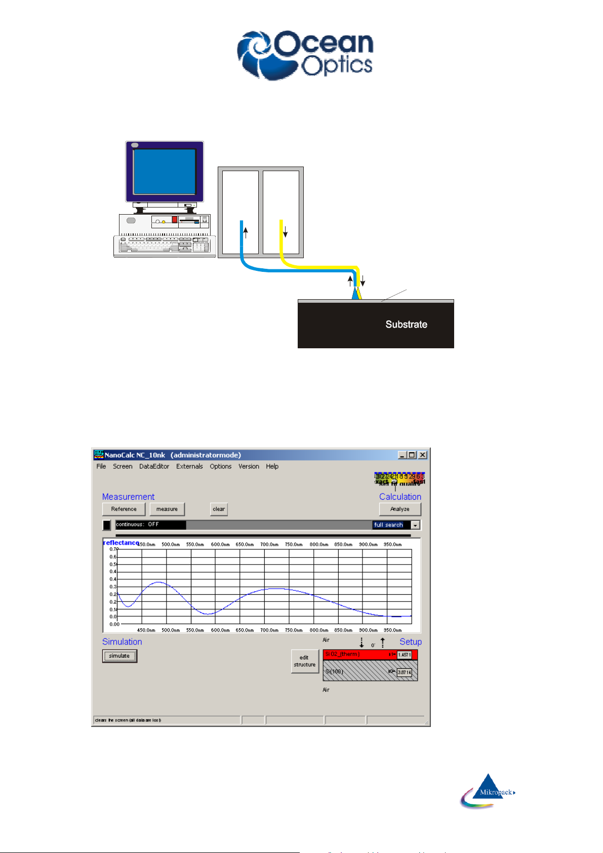
A
V
S
-
S
p
e
c
t
r
o
m
e
t
e
r
A
V
S
-
L
i
g
h
t
s
o
u
r
c
e
Fibercable
Thin Layer
NanoCalc-2000
1.1
Measurement setup
A broadband white light source is reflected by a thin layer under vertical incidence (after a calibration
measurement). The reflected intensity as a function of wavelength is measured by a spectrometer, a PC
extracts the wanted information.
1.2
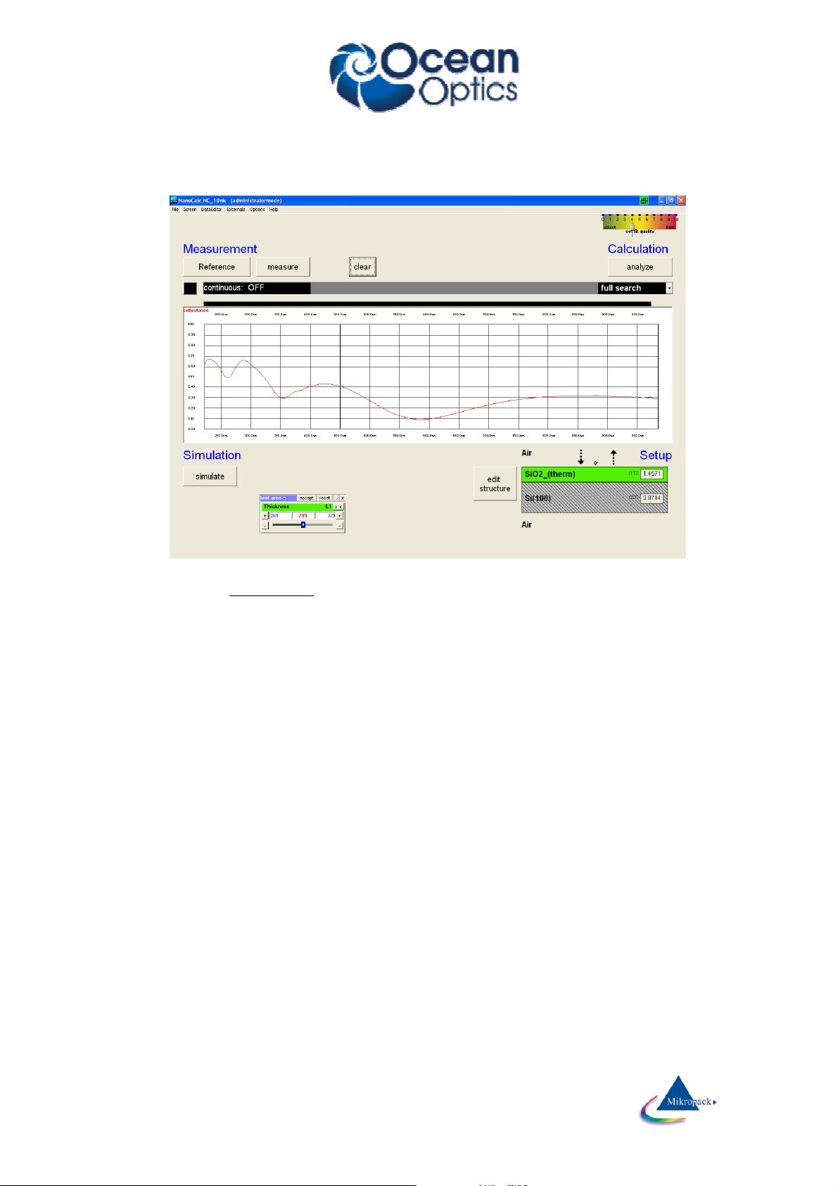
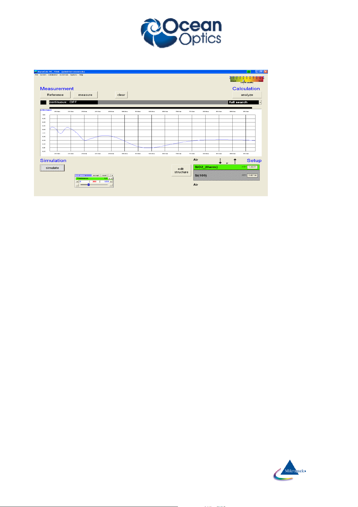
Measurement signal
The typical modulated signal of such a spectroscopic thin film measurement might look like this (after some
data manipulations):
NanoCalc uses this signal to extract thickness (eventually also dispersion) for this (SiO2 ) layer on Si.
Ocean Optics Germany GmbH Thin Film Metrology
4
Page 6
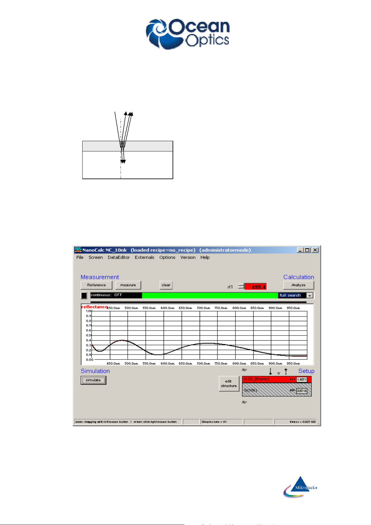
layer
1.3
Physical principle
The measurement principle of NanoCalc is the well-known fact of interference of light in thin layers. Light is
reflected (and transmitted), resulting in phase shifts and superposition of amplitudes and finally adding up to
different intensities for different wavelengths (=different colors). You see these colors in every-day-life, if you
observe the colors of thin oil films on water or if you carefully observe the colored anti-reflective coating on
lenses of cameras or binoculars.
substrate
transmitted (and
absorbed)
information: nearly vertical
incidence
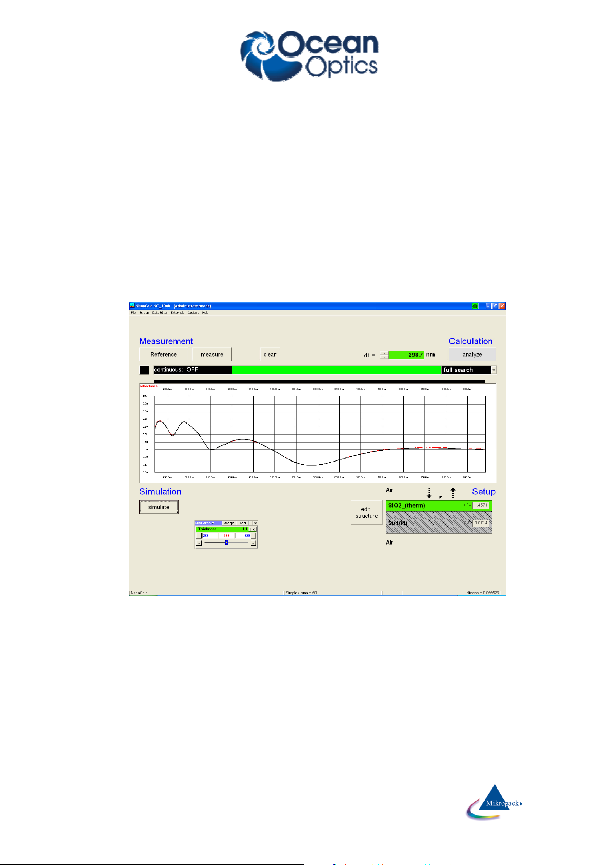
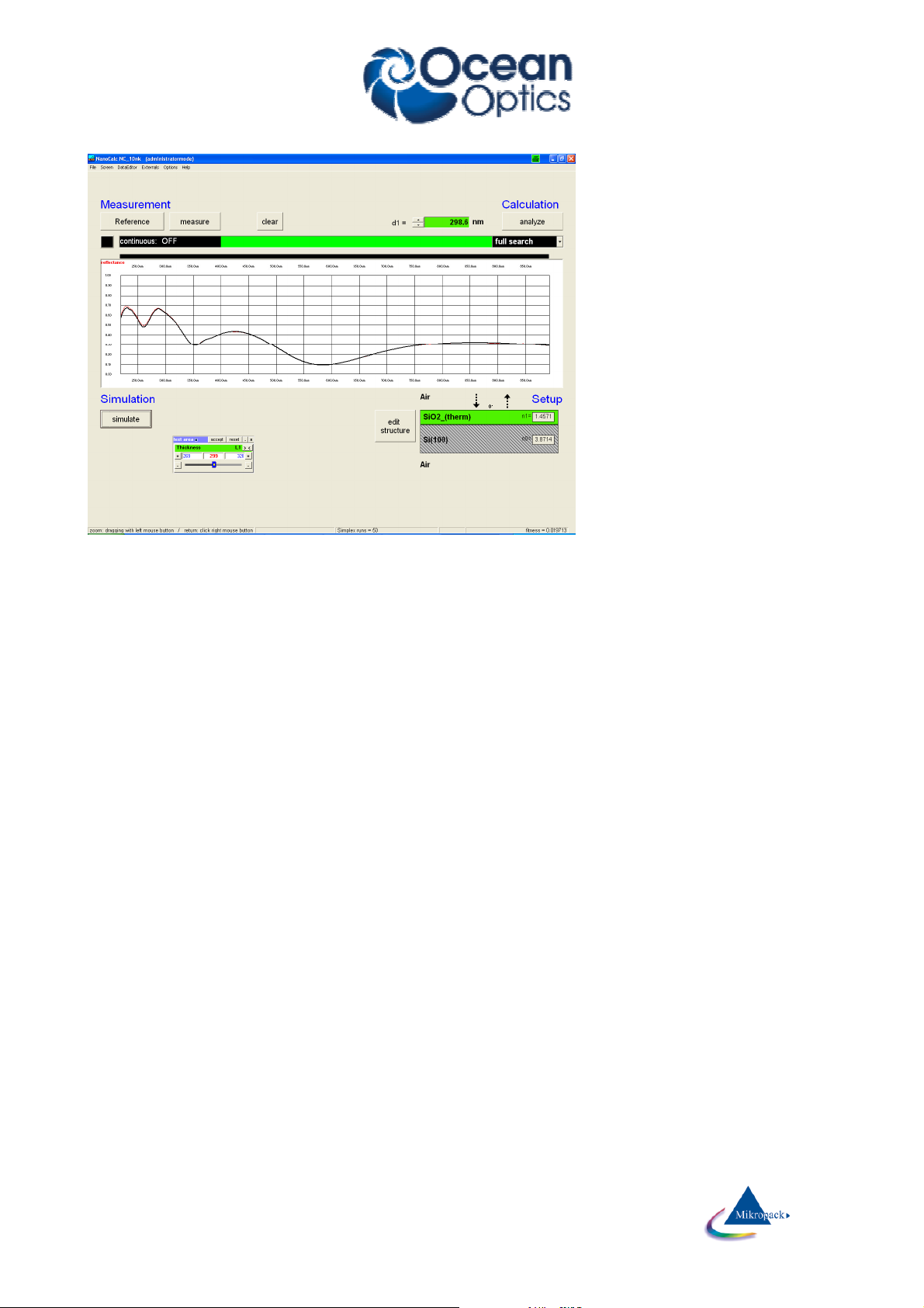
After some calculations NanoCalc will show a result (here: 499.4 nm) as the best fit to the experimental data
(red curve=measured signal, black curve = theoretical curve):
Ocean Optics Germany GmbH Thin Film Metrology
5
Page 7

2
Installation
NanoCalc (and SCOUT) is delivered on a CD-ROM.
Insert the CD-ROM in your CD-ROM drive and run „NanoCalc-Setup.exe “. Do not call “NanoCalc.exe” at
this level, if you happen to find it in some subdirectory.
NanoCalc will ask you for a directory (and propose a directory „c:\programs\NanoCalc“).
If you prefer other names, change this to "c:\MyPrograms\NanoCalc” or any convenient directory name).
Deinstallation:
If you want to deinstall NanoCalc from your computer, go to „system control“, „software“ and deinstall
NanoCalc.
Do NOT just delete it because NanoCalc adds some files to your windows\system directory and to the
registry !! Always de-install the software properly.
3
Product support
Please contact your local distributor for product support. Here you can find additional information:
www.OceanOptics.de
Ocean Optics Germany GmbH Thin Film Metrology
6
Page 8
4
Getting started
After installation of your hardware and software you should be ready to make your first measurements.
First example = without SCOUT-software:
1. You need a blank silicon wafer as a reference and a wafer with a thin layer (e.g. 495 nm SiO2 on Si). It
is a good idea to use a special “step wafer” with different oxide thickness as a first test or for calibration
purposes. Please ask your hardware supplier for information about step wafers.
Choose an experimental setup with a fiber or a microscope.
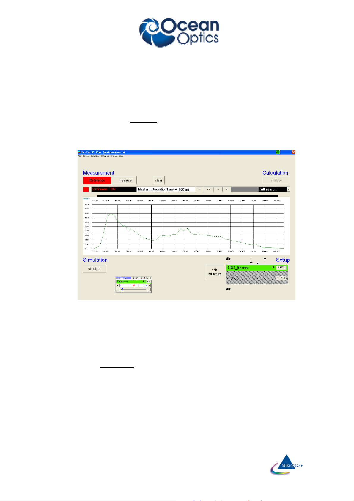
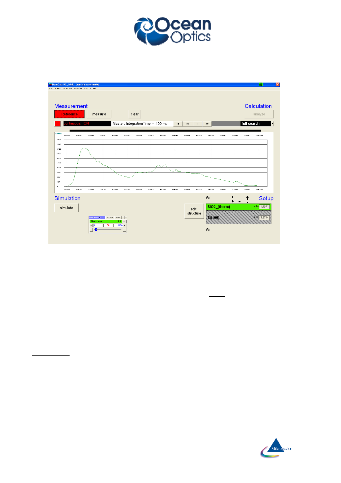
2. Then insert your reference wafer, switch on your lamp, start NanoCalc and click on the button
„continuous mode“.
This button turns RED. Then click on the button “reference” (this button turns RED as well) and you
should see the spectrum of your lamp as it measured repeatedly in short time intervals.
You should observe a spectral region comparable to the data of your spectrometer (e.g. 250 -1100 nm,
depending on your grating).
It is important to use a “good” amplitude of this signal = not too high and not too low. This means:
a. there should be no saturation of the CCD-detector (=a flat region) in the signal.
b. try to get a signal height of about 50-90% of the scale height for oxide samples (and similar) and
about 20% for metallic samples. The exact value is of no concern as long as your signal in the
measurement of the real sample does not cause saturation.
There are several possibilities to get a “good” signal amplitude:
a. increase or decrease integration time (with the buttons ±1 ms or ±10 ms) to adjust the signal
between 20-90%.
b. or adjust the lamp intensity (e.g.NanoCalc-VIS), if this is possible
3. Then click on the button „continuous mode“ again to turn off the continuous mode. Both buttons turn to
BLACK again. The last reference measurement is saved internally and you can see it on the screen.
Ocean Optics Germany GmbH Thin Film Metrology
7
Page 9
From now on there is no need to repeat this reference measurement unless you like to control
repeatability
BUT: from now on you should not change the lamp intensity or the distance to your sample. Your
sample should also have the same height as the reference sample.
4. Put your wafer with the thin film onto the stage and press the button „measure“. Pay attention not to
have dust particles in the region where you measure.
You should get a spectrum like this (with a different numbers of extrema or even no extrema).
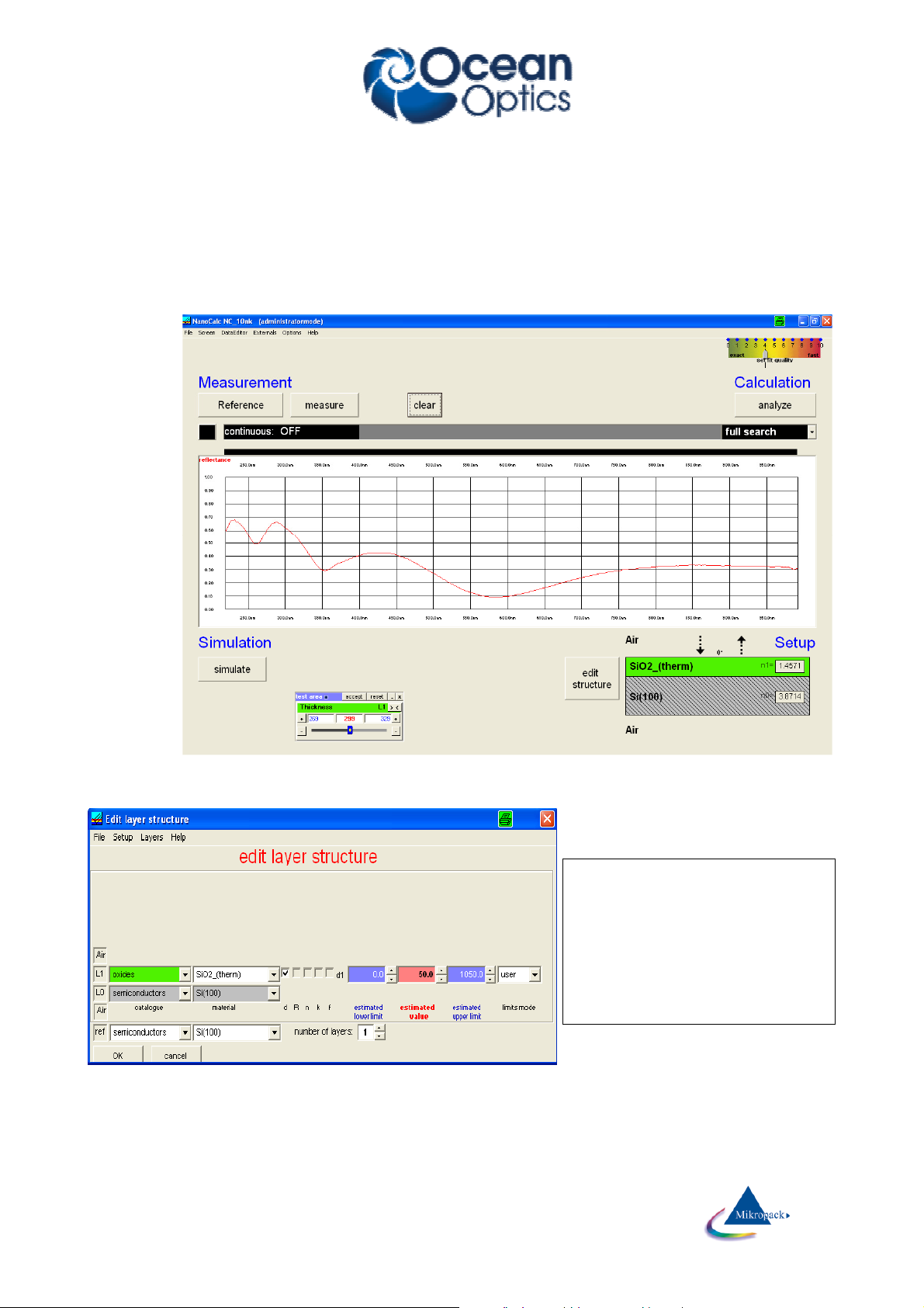
5. Then press the button „EditStructure“ and choose the correct parameters for your layer setup:
number of layers = 1
catalogue for substrate= semiconductors
catalogue for layer 1 = oxides
material for substrate = Si(100)
material for layer 1 = SiO2_(therm)
estimated thickness = 50 nm
user limits
It is not important to choose perfect values for thickness and estimation limits at the moment.
Ocean Optics Germany GmbH Thin Film Metrology
8
Page 10
When should you use “narrow limits” or “wide limits” or “user limits” ?
- if you have no knowledge about the thickness of your layer (but layer thickness should be MORE than
about 5 micrometers in thickness), choose "user limits"
- if you have no knowledge about the thickness of your layer (but layer thickness should be LESS than
about 5 micrometers in thickness), choose "wide limits"
- if you have GOOD knowledge about the thickness of your layer (within about 50-100 nm), choose
"narrow limits"
6. After changing the layer structure please check the spectral range again.
Use a smaller range for a thicker layer (and shifted more to VIS/NIR), and a range as wide as possible
for thin layers, e.g. 250 - 1100nm.
7. Press the button „analyze“. The result for the thickness of the oxide is shown in the upper right text
window.
Second example = with SCOUT-software:
Now it is assumed that you own the SCOUT software and want to use this powerful tool for extracting data.
This mode does not work, if SCOUT is not installed on your PC !
1. Get a reference spectrum in the same way as described above in steps 1 – 3
2. Now load an appropriate recipe with the menu “File\Load recipe”. You will be asked for the name of
the recipe. In the case of an oxidized silicon wafer we use the recipe: “Cauchy on Si.lrc” which is in
the list of delivered recipes. This recipe contains a Cauchy model for the dispersion n(λ) of SiO2 and
will also deliver the oxide thickness.
After loading this recipe you can see the layer structure. The button “EditStructure” is still accessible,
but it is only possible to change the reference material. All details of the layer system and all
Ocean Optics Germany GmbH Thin Film Metrology
9
Page 11

extraction limits etc are contained in the SCOUT recipe and can only be modified within SCOUT
(which needs some knowledge of optics and some experience with the SCOUT software)
3. Now press the button „analyze“. The result for the thickness and the refraction index of the oxide is
shown in the upper right text window. (comment: the thickness values for measurements with and
without SCOUT are slightly different because a Cauchy model is not the same dispersion as table
values)
Ocean Optics Germany GmbH Thin Film Metrology
10
Page 12
NanoCalc:
reflectometer
SCOUT
NanoCalc:
5
User modes of NanoCalc
NanoCalc has two different user modes, the “SCOUT-mode” and the “NanoCalc internal mode”. At the
moment the “internal-mode” is the normal mode, the “SCOUT mode” may be used but an extra SCOUT
software has to be purchased.
5.1
SCOUT mode
NanoCalc works as a graphical user interface for a sophisticated film software “SCOUT” working in the
background.
The whole process is necessarily driven by recipes.
• within NanoCalc you have to load a “recipe”, e.g. “SiO2 on Si.lrc”. This ASCII-readable recipe contains
a link to a SCOUT recipe like “SiO2 on Si.sc2”. All necessary layer informations are contained in this
SCOUT recipe and are read by NanoCalc, but only for display purposes.
• NanoCalc now controls the hardware, measures the sample and sends the measured reflectivity-values
to SCOUT (via a file NC_Data.xy in directory “NanoCalc\Internal_Files”).
• SCOUT does the calculation of all parameters
• the results are given back to NanoCalc via OLE-connection. The main fit parameters (thickness,
refraction, absorption, roughness and EMA-fractions) are displayed by NanoCalc, as well as all other
SCOUT fit parameters.
This SCOUT mode relies totally on good SCOUT recipes. So there must be someone (you or the
administrator or OceanOptics) in the background being familiar with the details and the physics of SCOUT.
The advantage is a “one-button-reflectometry” for the user and an enormous calculation power !
calculation
SCOUT sc2-recipe NanoCalc lrc-recipe
measure spectrum
display results
5.2
Internal mode
In this (normal) internal mode the user can create own layer stacks and does not need the external SCOUT
software at all. There is no need to work with recipes, but it is recommended. BUT: At the moment only
thickness values and a Cauchy dispersion can be extracted.
5.3
Combiversion with NanoCalc
If you bought a combiversion ElliCalc + NanoCalc (= ellipsometry and reflectometry) you will see an extra
menu “version”. Here you can switch from one application to the other.
Ocean Optics Germany GmbH Thin Film Metrology
11
NanoCalc lrc-recipe
define layer stack
measure spectrum
calculate thickness
display thickness
reflectometer
Page 13
5.4
List of all menus and buttons
Main menu Sub-menu SCOUT
mode
FILES menu Load file x
Load Scout layer recipe x x
Load NanoCalc layer recipe x x
Save as file x
Save as layer recipe x
Save as reference system x
Change layer recipe x
Save reference and dark x
Load reference and dark x
Export raw data x x
Import raw data x x
Show all results x
Print report x x
Exit x x
SCREEN menu Spectrometer data x x
Limits x x
Dispersion x x
Pixel resolution x
Show intensity x x
EXTERNALS Mapping x x
Analyze mapped data x x
Online/multipoint x x
Analyze online data x x
RS232 x x
Video camera x x
Show plot x x
OPTIONS Change buttons x x
Roughness (x) x
Special modes x
Fit parameters x
Some setups (overflow) x x
Some setups (change colors) x
Merasurement mode X x
Operator mode(Admin/User) x x
VERSION NanoCalc_1 x x
NanoCalc_10nk x x
ElliCalc x x
HELP Contents x x
About x x
EDITSTRUCTURE x
Internal
mode
Ocean Optics Germany GmbH Thin Film Metrology
12
Page 14
6
Basic features of NanoCalc
6.1
Reference
This button „freezes“ the reference spectrum and sets internal flags („there is a valid reference spectrum“).
So this spectrum is valid until you decide to measure again.
hint:
Pay attention not to run into saturation of the spectrometer ! (= a (nearly) horizontal part in the spectrum very
near to the upper limit of the plot). There is an option in menu “data extraction” to give a warning.
If you want to measure precisely (especially for extremely thin layers) repeat this reference from time to time
(drift of lamps and so on).
If you use a double spectrometer, you have to adjust the crossover wavelength. Below this wavelength the
data are collected from spectrometer channel A, above they are collected from spectrometer channel B.
You may use a different material for referencing than your substrate (but pay attention: do not run into
saturation in either mode !). In the present version a reference material has to be a solid, nontransparent
material like Si (where the optical constants n and k are well known.
If you choose a non-transparent material like glass (with a backside reflection !), NanoCalc will use a
different formula to calculate the reference reflectivity. In this case you have to choose a “thick” glass
(regarded as transparent), which means that the name of the glass material has to end with something like
“_1.5_mm”.
An example: you want to you use a thick BK7-plate with 2.3 mm thickness as a reference material. Then
rename the material “BK7.dat” in the materials directory to: “BK7_2.3_mm.dat”. Apart from that, please
regard that the quality of the glass surfaces on both sides is important.
There is an option for arbitrary reference systems.
Ocean Optics Germany GmbH Thin Film Metrology
13
Page 15
substrate
−
With:
6.2
Measure
This routine measures the spectrum of your test device and performs the following calculation:
Meas D
R R
Reflectivity:
As a result you get the theoretical reflectance (or transmittance) of your coated substrate.
If you are using a SCOUT-recipe the measured data are transferred to SCOUT. This takes some time ….
= ⋅
Ref D
−
Meas = measured spectrum
Ref = reference spectrum
D = dark spectrum
R
= reflectivity of an uncoated substrate
Substrate
Ocean Optics Germany GmbH Thin Film Metrology
14
Page 16
6.3
Simulate
This routine simulates a spectrum from the estimated thickness from „EditStructure“.
The structure that is simulated may be changed with button „EditStructure“, if you do not use SCOUT.
Otherwise you need SCOUT experience.
Hint:
If you want to have a short check which structure is simulated at the moment, put the mouse cursor over the
appropriate layer for some seconds and you see the layer thickness.
OR:
Leave your mouse cursor for some seconds over the button SIMULATE and look at the text in the status bar.
If you are using a SCOUT-recipe the calculation is done by SCOUT. This takes some time to transfer the
data…..
6.4
Analyze
This routine analyzes a spectrum (either simulated or measured) within the data extraction limits.
The structure that is simulated may be changed with button „EditStructure“, if you do not use SCOUT.
Ocean Optics Germany GmbH Thin Film Metrology
15
Page 17
Hint:
Leave your mouse cursor for some seconds
To have a short check which structure is
simulated at the moment, put the mouse
cursor over the appropriate layer for some
seconds and you see the layer thickness.
OR:
over the button SIMULATE and look at the
text in the status bar.
If you are using a SCOUT-recipe the calculation is done by SCOUT. This takes some time to transfer the
data…..
6.5
Continuous mode
The continuous button switches between continuous: ON (=red button) and “continuous: OFF” (button
=black). To use this option you have to switch either to “reference” or “measure” or “analyze”. Then there will
be a continuous measurement of the reference signal (very useful to adjust the intensity of your lamp) or
there will be a continuous measurement or even analyzing of your signal (very useful if you want to move
your sample to different positions).
All others buttons of NanoCalc are disabled until you finish the continuous mode.
You may adjust integration time by using the buttons -1/-10 /+1/+10 msec (separate for channel A and
channel B spectrometer)
6.6
Measurement mode
There are different data extraction modes in NanoCalc (internal mode):
Full search
NanoCalc uses the lower and upper limit of your guess in EditStructure and tries to find the best fit to the
measured values by testing all simulated curves in narrow intervals of 1 nanometer.
This is the preferable method in most cases, although it is not optimized concerning speed.
Fast search
NanoCalc extracts information from the (guessed) values in EditStructure to calculate thicknesses as precise
as possible. The search region is still determined by your choice of narrow, wide or user limits.
This is the fastest method in most cases, nevertheless it may fail.
Ocean Optics Germany GmbH Thin Film Metrology
16
Page 18

FFT
This method is very fast and applicable only for relatively thick layers, but not very precise !! It may be
refined by pressing the check box “use extended search after FFT or failure” in menu FitParameters.
You will see the fouriertransformed spectrum on the screen with different peaks. As your original signal is
NOT a sum of harmonic functions, there are peaks that do not correspond to a layer thickness (e.g. typically
there is a peak corresponding more or less to the sum of all thicknesses). All peaks that can be identified are
marked with a colored circle.
The scale in FFT mode is a scale of optical thickness (=product of geometrical thickness and refraction
index), not of geometrical thickness. If you SHIFT+Click on the values of refraction index (below the word
“SETUP” in main menu, the FFT scale will be recalculated for the value of the corresponding layer.
You have the choice between different options in menu EditStructure ("FixedLimits", "NarrowLimits",
"WideLimits" and "UserLimits")
"FixedLimitsMode"
In this mode the values of low and high limits of your estimate are made equal to the thickness. This
means that this layer is regarded as perfectly well-known.
Such a layer is excluded from data extraction algorithms.
"NarrowLimitsMode"
NanoCalc uses the value of your thickness estimation to calculate low and high limits which are quite
narrow (about ± 100 nm). A search is done ONLY within these limits. If your limits were to narrow this
search will fail and you have to try wider limits (like WideLimitsMode)
"WideLimitsMode"
The low limit and high limit is set according to the EditStructure setup menu:
1. relative wide limits: a symmetrical region is given, like ± 500 nm
2. absolute wide limits: the values of lower and upper wide limits are given as absolute values
In any case: a search is done ONLY within these limits. This means that the user does not need any
knowledge about the thickness. This option MAY be slow (but not necessarily !)
"UserLimitsMode"
NanoCalc fits the spectrum between low and high limits which were input by the user. Here the maximum
thickness is 300 micrometers.
Ocean Optics Germany GmbH Thin Film Metrology
17
Page 19

6.7
Fitness
Any extraction of parameters is accompanied by a value of "fitness". This is the sum of the mean square
deviations between measured and simulated curve (normalized to the range of extraction). The fitness is a
rough guide whether your thickness value is "good" or not.
In the file “Thinfilm.ini” you will find 3 entries in section [fit]:
Failure_RedLevel=1
Failure_YellowLevel=0.1
RYG_LevelsAreDisplayed=False
If you change the variable RYG_LevelsAreDisplayed from “False” to “True” (in main menu “Fitparameters”),
the usual rainbow pattern on the screen will disappear and a simple color will show up.
• If the fitness is below Failure_YellowLevel=0.1 you will see a GREEN color.
• If the fitness is between Failure_YellowLevel=0.1 and Failure_RedLevel=1 you will see a
YELLOW color.
• If the fitness is above Failure_RedLevel=0.1 you will see a RED color
Attention:
If you measure very thick layers (with a good correlation between maxima positions, but bad correlation
between signal heights) you may end up with high values of fitness, but nevertheless the thickness results
may be o.k.
Ocean Optics Germany GmbH Thin Film Metrology
18
Page 20
7
Detailed features of NanoCalc
7.1 Main menu “File”
Internal mode Scout mode
7.1.1
Load file
(internal mode only)
This routine loads a measured or simulated spectrum that has been saved earlier (extension: .nan). Do not
change the extension .nan.
It is assumed that all .nan-files are in the default directory “NanoCalc\data\nan_Files”, but you can change
the directory path to any other directory on your PC.
The *.nan-file is an ASCII file that contains most parameters of the software and the measured or simulated
values of reflectance (or transmittance) as a function of wavelength (or pixel) within the plot limits.
If you load a recipe instead of a *.nan–file you will not see any curve on the screen, but a change in the
setup or the limits. The only difference between a recipe and a *.nan-file is the additional list of data values.
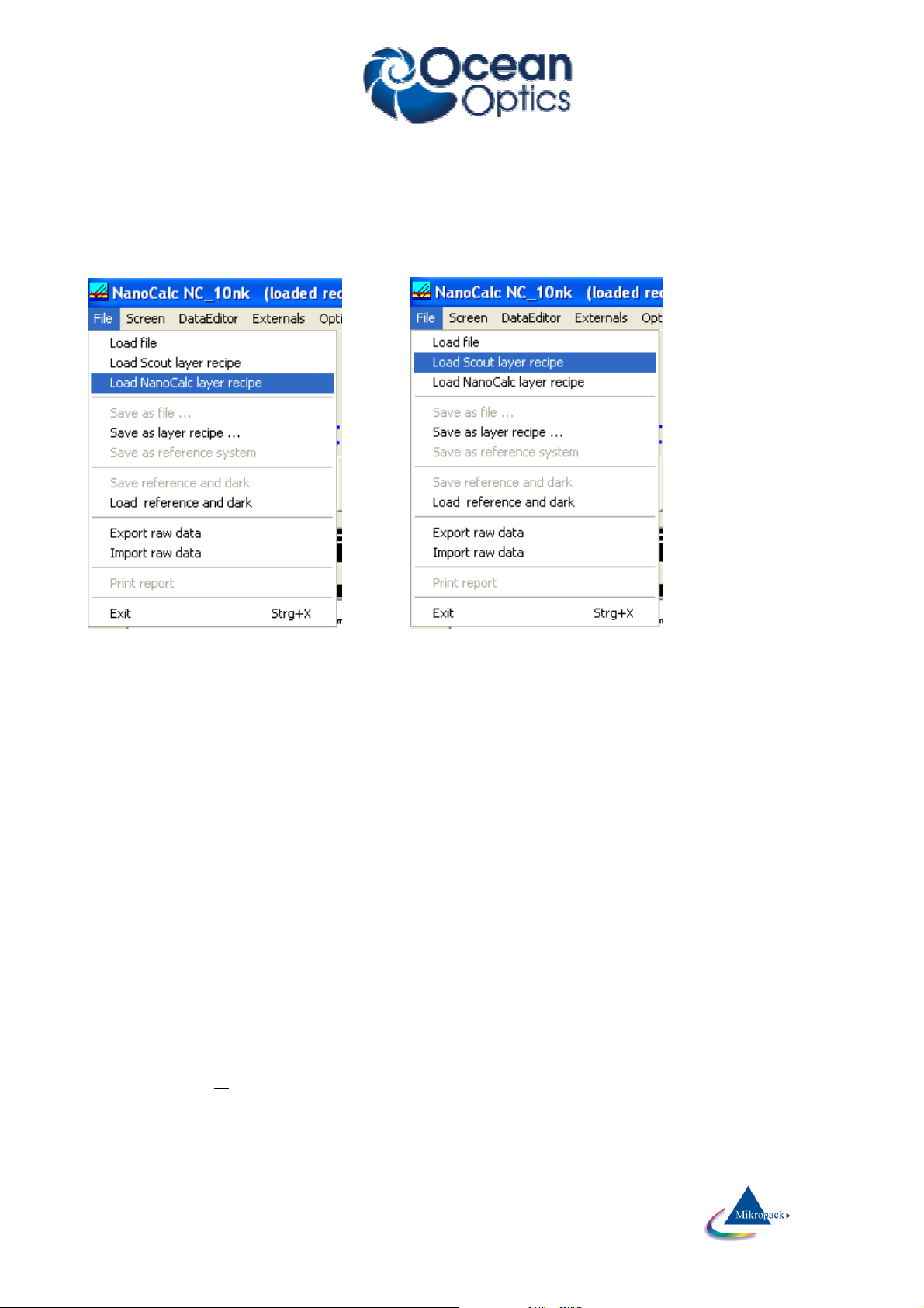
7.1.2
Load layer recipe
(internal mode and SCOUT mode)
This routine loads a layer recipe that has been saved earlier (extension: .lrc). Do not change the extension
.lrc.
In SCOUT mode you may either load another SCOUT recipe (“load Scout layer recipe”) or you may switch
to NanoCalcs internal mode (“Load NanoCalc layer recipe”). See the screenshots above.
In SCOUT mode all buttons captions are in italic, otherwise in normal.
It is assumed that all .lrc-files are in the default directory “NanoCalc\recipes\layer_recipes”, but you can
change the directory path to any other directory on your PC (provided that you did not use
"UseLastFilenames_NC=False" in section [Filenames_NC] in Thinfilm.ini).
Ocean Optics Germany GmbH Thin Film Metrology
19
Page 21

There is a section [Scout] in this layer recipe with an entry for "Scout_Recipename_NC". This entry is a
link to the corresponding SCOUT .sc2-recipe in the directory "c:\programs\scout\scout_sc2_recipes" (or
similar directory name).
If this linked .sc2-recipe is existent, SCOUT will be used for calculations = “SCOUT mode”. If this link is
empty, NanoCalc will calculate without SCOUT = “internal mode” (at the moment only for thicknesses and
Cauchy parameters !)
Example for SCOUT-mode (in ellipsometry):
[Scout]
Scout_DirPath=c:\programs\scout
ScoutStopTime=15
Scout_RecipeName_NC=SiO2 (table) on Si.sc2
Scout_RecipeName_EC=
Example for NanoCalc internal mode:
[Scout]
Scout_DirPath=c:\programs\scout
ScoutStopTime=15
Scout_RecipeName_NC=
Scout_RecipeName_EC=
The *.lrc-file is an ASCII file that contains most parameters of the software, but NO measured or simulated
values of psi/delta (or tan(psi) /cos(delta)) as a function of the wavelength.
If you load a recipe you will not see any curve on the screen, but a change in the setup or the limits.
7.1.3
Save as file
(internal mode only)
This routine saves the measured or simulated file as an ASCII file with the extension .nan. The name of the
file may be chosen arbitrarily. Do not use any other extension than .nan.
The *.nan-file is an ASCII file which contains most parameters of the installation and reflectivity R(λ) as a
function of wavelength (or pixel) within the plot limits.
7.1.4
Save as layer recipe
(internal mode only)
Ocean Optics Germany GmbH Thin Film Metrology
20
Page 22

This routine saves all layer and screen settings as an ASCII file with the extension .lrc. The name of the file
may be chosen arbitrarily. Do not use any other extension than .lrc.
The *.lrc-file is an ASCII file which does NOT contain and reflectivity R(λ) as a function of wavelength (or
pixel) within the plot limits.
7.1.5
Save reference and dark
(internal mode and SCOUT mode)
This routine saves the current reference data to the file “NanoCalc\data\ref_files\name.ref” and/or to
“NanoCalc\data\ref_files\name_pixel.ref”. If the screen was switched to pixel resolution both of these files are
saved.
If the dark button was active also 1-2 dark files are saved
This function is easily accessible through function key F8.
7.1.6
Save as reference system
(internal mode only)
In Version NC_10nk there is an option to use “reference systems”. e.g. a glass reference with a backside
surface or even a stack of layers (e.g. native oxide). First you have to measure this reference system in the
normal way = with silicon as reference. Then press the button file/save as reference system. Then choose
this system as a new reference in EditStructure.
7.1.7
Load reference and dark
(internal mode and SCOUT mode)
This routine loads a reference from the directory “NanoCalc\data\ref_files”. If you choose to load a pixel
reference, both references will be loaded (eventually also dark files)
Which of these two files is displayed depends on the pixel or nanometers resolution.
This function is easily accessible through function key F9.
7.1.8
Load last measurement
(internal mode only)
This function is easily accessible through function key F11.
7.1.9
Load last saved file
(internal mode only)
This function is easily accessible through function key F12.
7.1.10
Import raw data
(internal mode and SCOUT mode)
You are asked for an import- directory. The imported values are displayed in blue (=similar to measured
values). The scale of the screen is not adjusted.
7.1.11
Export raw data
(internal mode and SCOUT mode)
If a curve was produced by simulation or measurement it may be exported as ASCC-file (“raw data”). This
file has a very simple structure: (lambda, value)
350,0.455
351,0.467
352,0.479
353,0.490
354,0.501
355,0.512
356,0.522
You are asked for a directory to save this file. Please use the default directory \RawData_Files\Reflectometry
Ocean Optics Germany GmbH Thin Film Metrology
21
Page 23

7.1.12
Print report
This routine allows you to enter some user data (names of operator, of sample and so on), shows a preview
and prints on the Windows standard printer. Changing the printer is possible only within Windows itself.
Entering of user data: you may also change the names of the labels (empty labels: this line is not shown on
the final print). In the preview window you may zoom in and out. After pressing the print button you have the
chance to change some printer options.
If you want to get a printout of the complete screen or parts of it:
It is recommended to use a hardcopy program to print the different parts of the software with enough
options to change colors, resolution etc.
We recommend a shareware ”HC.EXE” (http://www.sw4you.de and on the CD-ROM in : tools\general),
which will include a small button in every (!) window of your system near to the close button.
For online-users: we recommend to buy the OPTION NanoCalc-Online for printouts of Multipoint
Measurement, Result-Windows with Statistic Data’s and Excel-Connection.
7.1.13
Show all results
(SCOUT mode only)
See chapter “Special features for SCOUT mode”
7.1.14
Exit
This routine exits NanoCalc and SCOUT and closes all windows. All important data have been written to
the Thinfilm.ini -file before and will be reloaded in the next run.
Important warning:
Do NOT close SCOUT separately !!! This would break the OLE-connection between SCOUT and
NanoCalc. The only way to restore this connection is to exit NanoCalc and restart the software !
7.1.15
Function keys
If you click on the buttons F2 - F7 different spectra or recipes together with their layer data are loaded (for
demonstration purposes or to get a faster access to recipes than by loading them via “files\load recipe”). You
should be able to analyze these demonstration spectra by a simple click on the button “analyze”.
How to add your own recipes to function keys:
Step 1: carefully adjust all parameters in EditStructure and all plot and extraction limits. Do not forget
roughness parameters if necessary.
Step 2: save this setup with menu “files\save_as_recipe” as usual BUT save it to menu “data\internal_files”
instead of saving it to menu “recipes\layer_recipes” AND save your setup with the name of the function key,
e.g. save F4.nan or F6.nan (NOT F6.lrc !!). Recipes stored in function keys have the file extension .nan and
not the extension .lrc (as usual layer recipes). Check for correct names with Windows Explorer !
Ocean Optics Germany GmbH Thin Film Metrology
22
Page 24
7.2
Main menu “Screen”
7.2.1
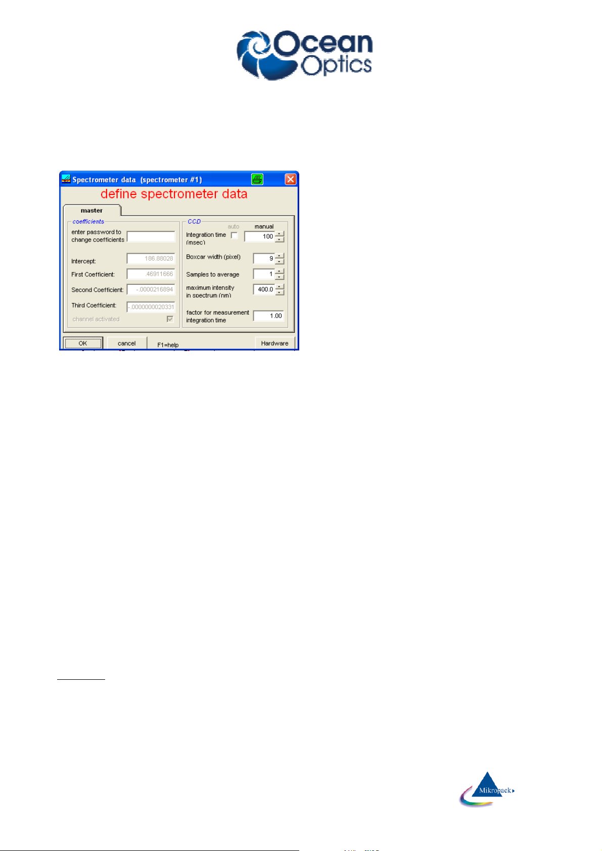
Spectrometer data
The 4 spectrometer coefficients are displayed for
information purposes. They are automatically set by
the Thinfilm.ini file which is specific for each single
system.
Changing these values will screw up the system and
is therefore password protected and only accessible
for technical service.
For calibration purposes you may change these
values (with a password and only within several
percent deviation from your original values).
physical meaning:
These 4 numbers are the coefficients in a formula that shows the dependence between wavelength (in
nanometers) and pixel number of your spectrometer according to the following formula:
λ
with:
I = intercept
C
C2 = second coefficient
C
P = pixel number
Hint: Ask your hardware supplier if you have the impression that it might be necessary to recalibrate the
spectrometer (a red HeNe-laser should show 632.8 nm)
= first coefficient
1
= third coefficient
3
2
21
3
PCPCPCI ⋅+⋅+⋅+=
3
7.2.1.1 Integration time
Whenever you change this value, it is written to disk (in file “Thinfilm.ini”) and will be used as a startup value.
How to change integration time:
1. method:
To check integration time rapidly, use continuous mode button. You may change the value of integration time
by +1 msec or +10 msec or -1 msec or -10 msec within a mouse click. Try to achieve a maximum signal of
20 - 90 % of total range. This value will depend very much on the reflectivities of your reference materials,
your substrate material and your layer material.
Ocean Optics Germany GmbH Thin Film Metrology
23
Page 25

An example:
If you use silicon as reference and substrate material and you want to measured silicon oxide thickness you
should try to get reference signals of 80 - 90 %. An oxidized silicon wafer will NOT produce signal saturation
and your signal-to-noise-ration will be as high as possible.
If you use a metalized surface as a reference (and you want to measure oxidized silicon wafers later on) you
need to start with LOW reference intensities (like 20 %) to avoid saturation in your measured signal. Of
course you get a lower signal-to-noise-ratio in this case.
After switching off continuous mode button, you do not have to press the reference button again as the last
signal has been saved.
2. method:
use the menu "options/spectrometer data" and check by pressing the reference button once.
Tips:
Try to use short values of integration time while keeping the lamp intensity as high as possible (to get short
measuring times). This is especially important in mapping mode.
If your integration times are too short, you will have problems with signal-to-noise. If your integration times
are too long, you will get saturation of the signal and this may cause errors in data extraction.
You may check the value of integration time at any time without entering the menu OPTIONS: Put your
mouse cursor over the button “reference” or “measure” and wait for about 2 seconds: a small window will
pop up to inform you about integration time, samples to average and boxcar width.
These values correspond to the channel A spectrometer if you use a double spectrometer.
7.2.1.2 Boxcar width
physical meaning:
The Ocean Optics spectrometer is able to average over some pixels to increase signal/noise-ratio.
A boxcar width of 1 pixel means no averaging at all. This has to be used if you want to measure very thick
layers (like 50 micrometers of resist)
A boxcar width of 5 pixels means an averaging over 2 pixels on the left side and 2 pixels on the right side (=
5 pixels altogether). This averaging routine is shifted from the left side of the simulated spectrum to the right
side with a step size of 1 pixel only. Values of 5-9 are recommended if you want to measure films in the
range of 1 micrometer or less as you get a better signal-to-noise ratio. Use a value of 1 for very thick layers.
hint:
You may check boxcar width at any instance without entering the menu OPTIONS: Put your mouse cursor
over the button “reference” or “measure” and wait for about 2 seconds: a small window will pop up to inform
you about integration time, samples to average and boxcar width.
These values correspond to the channel A spectrometer if you use a double spectrometer.
7.2.1.3 Samples to average
Whenever you change this value, it is written to disk (in file “Thinfilm.ini”) and will be used as a startup value.
physical meaning:
The Ocean Optics spectrometer is able to average over some runs to increase signal/noise-ratio.
Tips:
Try to use small values for Samples To Average while keeping the lamp intensity as high as possible (to get
short measuring times). This is especially important in mapping mode.
You may check Samples To Average at any instance without entering the menu OPTIONS: Put your mouse
cursor over the button “reference” or “measure” and wait for about 2 seconds: a small window will pop up to
inform you about integration time, samples to average and boxcar width.
Ocean Optics Germany GmbH Thin Film Metrology
24
Page 26

7.2.1.4 Internal correct for dark
If you choose this option, dark current is corrected automatically (see Button “measure”).
The Ocean Optics Spectrometer is able to the dynamic dark current internally within a couple of pixels that
are NOT irradiated by external light, and is correcting dynamically.
7.2.1.5 Dark button
If you choose this option, dark current is corrected mathematically. This is necessary if you can’t protect your
system against ambient light or stray light.
7.2.1.6 Maximum intensity
This value describes the maximum intensity in the spectrum of your (halogen ?) lamp.
This value helps NanoCalc to achieve an automatic adjustment of the reference spectrum within the limits of
the screen (=without saturation)
If you use a double spectrometer there are TWO such wavelengths corresponding to the different
sensitivities of the two spectrometers and your light source.
7.2.1.7 Crossover wavelength
If you use a double spectrometer with different sensitivity regions (e.g. 200-600 nm for the CHANNEL A
spectrometer and 500-1100 nm for the CHANNEL B spectrometer), NanoCalc
single spectrum (200 -1100 nm). The wavelength where the two overlapping spectra are joined is called
crossover wavelength. (any value in your overlap range of the two channels is possible, 550 nm would be a
good choice in this case).
joins the 2 spectra to get a
7.2.2
Limits
The spectrometer limits in magenta colors are showing the maximum range of your specific system.
Ocean Optics Germany GmbH Thin Film Metrology
25
Page 27

7.2.3.1 Plot limits
The plot limits are the left and right side of the plot on your screen and coincide with limits of measurement.
The adjustable values of the plot limits depend on the grating in your Ocean Optics Spectrometer and are
noted in the calibration sheet of your system.
The plot limits may be changed within NanoCalc in steps of 1 nm.
1. normal mode to change the limits:
open the menu “spectrometer data \ limits” and enter numbers or use the up-down arrows
2. fast and rough method to change the limits:
If you click in the field near the
LOWER numbers you may change the plot limits without entering the
menu option/limits:
If you click in the LEFT half with your LEFT mouse button you will decrease the lower plot limit.
If you click in the LEFT half with your RIGHT mouse button you will increase the lower plot limit.
If you click in the RIGHT half with your LEFT mouse button you will decrease the lower plot limit.
If you click in the RIGHT half with your RIGHT mouse button you will increase the lower plot limit.
The same feature applies to plot limits and reflectivity limits.
3. fast and precise method to change the limits:
If you move your mouse very near to the lower part of the plot window (but still in the grey part) you will
see a little vertical arrow and the value of the wavelength is displayed. If you now click with the left mouse
button, you are able to change the lower plot limit (right mouse button=upper plot limit). The same applies
to the other 2 grey zones = extraction and reflectivity limits (see picture)
4. Zoom
You may zoom by
dragging the mouse from
one point to another
within the plot area.
If you click with the right
mouse button a small
popup window will appear
with the chance to undo
this zoom.
You can also change the
plot limits back to the full
range (according to your
spectrometer limitations).
You can also set the
current plot limits as a
standard or return to a
previously set standard.
ATTENTION:
To be consistent with data handling, ALL materials files contain n and k data between 150 nm and 1100
nm. Usually only parts of these data are measured data (e.g. between 206 nm and 840 nm or between
300 nm and 1100 nm). If you simulate, the valid part of the curve is shown in black while the rest is shown
in grey (and you get a message).
Extraction limits are restricted to the range of valid n and k data.
Ocean Optics Germany GmbH Thin Film Metrology
26
Page 28

7.2.3.2 Extraction limits
These limits cannot be larger than the plot limits. Try to use a large extraction range as long as your signal is
“good”.
1. normal mode to change the limits:
open the menu “spectrometer data \ limits” and enter numbers or use the up-down arrows
2. fast and rough method to change the limits:
If you click in the field near the UPPER numbers you may change the extraction limits without entering
the menu “spectrometer data \ limits”.
If you click in the
If you click in the LEFT half with your RIGHT mouse button you will decrease the lower extraction limit.
If you click in the RIGHT half with your LEFT mouse button you will decrease the lower extraction limit.
If you click in the RIGHT half with your RIGHT mouse button you will decrease the lower extraction limit.
The same feature applies to plot limits and reflectivity limits.
3. Fast and precise method to change the limits:
If you move your mouse very near to the upper part of the plot window (but still in the grey part) you will
see a little vertical arrow and the value of the wavelength is displayed. If you now click with the left mouse
button, you are able to change the lower extraction limit (right mouse button=upper extraction limit)
ATTENTION:
To be consistent with data handling, ALL materials files contain n and k data between 150 nm and 1100 nm.
Usually only parts of these data are measured data (e.g. between 206 nm and 840 nm or between 300 nm
and 1100 nm).
If you simulate, the valid part of the curve is shown in black while the rest is shown in grey (and you get a
message).
Extraction limits are restricted to the range of valid n and k data.
LEFT half with your LEFT mouse button you will decrease the lower extraction limit.
7.2.3.3 Reflectivity limits
Reflectance (and transmittance) are defined between 0 and 1.
To zoom in the plot and to see some more details you may change the reflectivity limits. In most cases you
will not need this option.
1. normal mode to change the limits:
open the menu “spectrometer data \ limits” and enter numbers or use the up-down arrows
2. fast and rough method to change the limits:
If you click in the field near the LEFT numbers you may change the reflectivity limits without entering the
menu option \ limits:
If you click in the LOWER half with your LEFT mouse button you will decrease the lower reflectivity limit.
If you click in the LOWER half with your RIGHT mouse button you will decrease the lower reflectivity limit.
If you click in the UPPER half with your LEFT mouse button you will decrease the lower reflectivity limit.
If you click in the UPPER half with your RIGHT mouse button you will decrease the lower reflectivity limit.
The same feature applies to plot limits and reflectivity limits.
3. Fast and precise method to change the limits:
If you move your mouse very near to the left part of the plot window (but still in the grey area) you will see
a little horizontal arrow and the value of the wavelength is displayed. If you now click with the left mouse
button, you are able to change the lower reflectivity limit (right mouse button=upper reflectivity limit)
7.2.4
Dispersion
This form shows the refraction index n(lambda) and the absorption index k(lambda) (within the plot limits) for
different layers.
This form is just a tool to control your data, nothing can be changed in this form.
Ocean Optics Germany GmbH Thin Film Metrology
27
Page 29

• You may use 2 cursors (symbol #4). At start time of the cursors both cursors are painted on top of
one another, move them with the mouse. The cursor values are shown in blue (= k(λ)) and red (=n(λ))
• You may also zoom in and out and in an area (symbols #1 - #3)
You may also save these dispersion values
as a dat-file, but be very careful about the
target directory !!
ATTENTION:
To be consistent with data handling, ALL materials files contain n and k data between 150 nm and 1100 nm.
Usually only parts of these data are measured data (e.g. between 206 nm and 840 nm or between 300 nm
and 1100 nm).
If you simulate, the valid part of the curve is shown in black while the rest is shown in grey (and you get a
message).
Extraction limits are restricted to the range of valid n and k data.
7.2.5
Pixel resolution
This option is only useful for very thick films. If you use the option pixel resolution the software will acquire
and display all data in spectrometer pixels and no more in nanometer resolution.
With pixel resolution data are displayed at exactly those wavelengths where there is a pixel in your
spectrometer. If you own a high resolution spectrometer there is a spectral resolution down to 0.2 nanometer
or less. For more precise information consult your hardware supplier.
The same option is also accessible via menu “data extraction \ sampling”.
Ocean Optics Germany GmbH Thin Film Metrology
28
Page 30

7.2.6
Show intensity
If you use this option you will observe a value of ”total intensity” in one of the panels in the status bar. This
value is just the sum of all intensities between the extraction limit with a spacing of 5 nm.
Example:
I(total)=234.45
So this figure gives a very rough information about the area under the measured or simulated curve. This
might be used to maximize some intensity.
Ocean Optics Germany GmbH Thin Film Metrology
29
Page 31

7.3
Main menu “Data Editor”
7.3.1
Modify old .dat-files
Modifying existing dat-files:
1. At first you will see two combo-boxes to choose a catalogue and a material.
2. Then click “open file”. Some new features become visible: either a list with cauchy coefficients or a table
with dispersion data
If you like to change these old data (=adding of constants or multiplying with a factor), just click on ADD
or MULTIPLY in the appropriate row. It is possible to change each cauchy coefficient separately, but not
a single value in a table. If you want to change table values, you have to do this with an external text
editor.
3. After adding or multiplying click on “save dat-file” or click “reset modifications”
Then the software will automatically switch to the page “save dat-file”.
7.3.2
Save DAT-files
Be careful where you save this “new” material !
Ocean Optics Germany GmbH Thin Film Metrology
30
Page 32

7.3.3
Create Cauchy .dat-file
Creating new Cauchy dat-files:
It is only possible to create new DATfiles with cauchy coefficients, not as a
table of index data. To create a table you
have to use an external text editor.
1. At first you will see three
wavelengths and 6 Cauchy
coefficients n0, n1, n2, k0, k1and k2
2. change these values according to
your information. You have to add
ALL three values.
3. click on create Cauchy coefficients
4. then click on “save DAT-file” or click
“reset modifications”
Then the software will automatically
switch to the page “save DAT-file”.
7.3.4
Create EMA dat-file
Creating new EMA dat-files:
An EMA-file is a mixture of 2 different dispersion
values. There are different mixture algorithms in the
literature. In NanoCalc only the simple Looyenga
method (=a linear mixture) and the Bruggeman
method are implemented.
The structure of an EMA dat-file is rather similar to 2
added normal dat-files. Here you see an example for
Poly-silicon as a mixture of crystalline silicon and
amorphous silicon (it is also possible to construct such
a file manually with every text editor)
Si_cr.100(Aspnes_mod.)
633,3.8714,0.0158
150,1100
EMA_Mixture=Si_(100),a_Si,Bruggeman,50.0_Perc
ent
Table
150,0.5100,2.1500
151,0.5000,2.1500
152,0.5000,2.1500
….
Ocean Optics Germany GmbH Thin Film Metrology
31
Page 33

…
….
1098,3.5559,0.0014
1099,3.5557,0.0014
1100,3.5554,0.0014
a_Si(SOPRA_amorphousSilicon)
633,4.517,0.2312
240,840
EMA_Mixture=Si_(100),a_Si,Bruggeman,50.0_Percent
Table
150,1.6844,3.3312
151,1.6844,3.3312
152,1.6844,3.3312
153,1.6844,3.3312
154,1.6844,3.3312
Be careful where you save this “new” material !
Ocean Optics Germany GmbH Thin Film Metrology
32
Page 34

7.4
Main menu “Externals”
7.4.1
Mapping
You need a mapping-xy-stage and a special mapping
add-on software for NanoCalc to measure in mapping
mode. In this mode it is possible to measure and
display your film parameters as a function of x and y.
Ocean Optics Germany GmbH Thin Film Metrology
33
Page 35

main menus of mapping mode
1. menu “Recipes”
• Save as map recipe
• Load map recipe
Here you may save or load ALL the settings you have done in all the various possibilities. It is
recommended to save your usual settings in a recipe. It is possible to use a special recipe name like
“myownRecipe”. Recipes for mapping will receive the extension “.mrc” and will be saved in menu
“Recipes\Map_Recipes”
2. menu “Teach in”
This will be explained later in a following section
3. menu “help”
this is the usual access to help functions
main buttons (lower right side)
reference
you can take a reference with a blank reference wafer (right mouse button=time adjuastments possible)
measure
you can take a real (test) measurement with your sample. Thus you can control all settings before you
start the mapping
clear
clears the screen
Ocean Optics Germany GmbH Thin Film Metrology
34
Page 36

scan mode:
analyze
you can analyze the layer thickness your sample. Thus you can control all settings before you start the
mapping
conti
you can take a reference or a measurement in continuous mode.
initialize stage:
After starting mapping mode you have to initialize the mapping stage first.
Until the mapping stage is initialized the function start mapping is deactivated.
start mapping
this will start the mapping sequence
cancel
leave mapping mode
a. shape of the wafers:
1. You may use square or round wafers.
2. To use your own design as a background you need to edit the file
OwnDesign.bmp (this is possible with lots of drawing programs or ask
your software supplier for help).
b. wafer size
Wafer size may be changed between 50 mm and 300 mm (= 12'').
A grid is shown with a constant grid distance (e.g. 10 mm).
c. scan region
It is possible to change:
-
the x and y coordinates of the origin in steps of 0.1 mm
-
the number of rows and the number of columns of the scanning grid
(from 1 to 100)
-
the size of the x and y steps (in multiples of 0.1 mm)
The wafer plot shows what you are doing.
d. rotation
here you can rotate the scan region
Ocean Optics Germany GmbH Thin Film Metrology
35
Page 37

e. mapping positions
wafer:
measuring position:
If you press one of the position buttons (Home, Scan, Center, Reference), the mapping stage will immediately go to
this point and a red circle is displayed on the screen. Additionally the coordinates of this point are displayed. If
option "measure on each click" in Tab2 is activated, a measurement will be performed.
You may reach any point by clicking with the LEFT mouse button or by entering the coordinates and pressing the
xy-button.
You may move up and down or left and right by pressing the appropriate arrow buttons. If you press the arrow
buttons with the left mouse button the cursor will move in increments of xSteps. If you press the arrow buttons with
the right mouse button the cursor will move in smaller increments of xSteps/10
f. position buttons:
1. home position
Usually this is in the right lower corner of the xy-stage. The hardware of the stage will define this point at the
beginning of the mapping experiment (and it can be changed manually in the ini-File in section [mapping],
HomepositionX/Y=.... The numbers mean the percentage compared to wafersize (0.05 =5% of wafersize)
2. scan position
this is the origin of the scanning coordinate system
3. center position
this is the center of the (round) wafer stage
4. reference position
this is the position where the reference measurement has to be done.
this point (=the black circle) may be chosen by clicking with the RIGHT mouse button or by changing the
numbers
The wafer plot shows what you are doing.
The shape of the substrate may be:
a. circular (between 50 and 300mm)
b. square (between 50 and 300 mm)
c. your own design (change file "OwnDesign.bmp" with any drawing
software)
example:
Wafer size may be changed between 50 mm (= 2'' ) and 300 mm (= 12” ).
Ocean Optics Germany GmbH Thin Film Metrology
36
Page 38

Xy-stage:
data extract:
Ocean Optics can deliver xy-stages up to 300mm
(= 12”)
a. xy reference position
With a right mouse button click you may change the position for measuring
the reference. You may also enter numbers in this field. There is a
possibility to build a wafer-chuck with a special area for a piece of
reference-material even outside the defined wafer area. You may enter
negative coordinates, but be VERY careful not to damage the stage. When
the reference is taken, the stage drives to the set reference position and
takes the reference measurement.
b. xy center position:
You may define a round (!) area which means the area of measurements.
This area is not necessarily the same as the reserved area for the chuck
c. wait interval:
After each measurement the scanning may be interrupted for a certain
interval of time
d. scanmode:
If you activate this option each single measurement is waiting for a trigger
signal (a keystroke with ENTER key or an external TTL trigger signal which
is applied to the spectrometer. Ask your hardware supplier…)
a. visibility during map
You have the choice between 1D-plots for line scans, 2D-plots and/or 3Dplots. The 2D-plot and the 3D-plot contain the same data.
A 1D-plot is possible only if you measure along ONE row or column (and
not a two-dimensional field.)
Only one variable is allowed to be seen during map.
b. analyzing options
Analyze thickness on each left mouse click. This is a very useful feature
to make a quick check on thickness distributions on your wafer (do not
forget to activate option "plot value ").
Fitness limit: if your results are completely wrong for some reasons, all
measured values with a fitness greater than this fitness limit here will be
set to zero. This feature is useful, if dust causes a measurement error
during mapping. Without this feature you might get enormous spikes.
d. number of runs
You have the choice between a single run (for real measurement
purposes) and a nearly infinite number of runs (=30000) for
demonstration purposes.
Ocean Optics Germany GmbH Thin Film Metrology
37
Page 39

data export:
Scan data:
You may choose the following options during a mapping experiment:
1. plot the simulated curve
2. plot thickness value
It is more informative to see the analyzed curve and the calculated value of
thickness during the simulation, but this is time-consuming. If the mapping
takes a longer time it is recommended to switch off these 2 features.
You may choose the following options after a mapping experiment:
1. write data as map-file
2. insert comments in map or Excel-files
3. show results window
1. Write data as map-file
All thickness and fitness data together with some coordinate information
are written to a ASCII-file in directory “NanoCalc\data\map_files”.
examples can be found in the directory “NanoCalc\data\map_Files”
2. insert comments in map or Excel-files
You may enter text like “sample #1, “Paul McCartney” or “myfirsttest”.
This text will be a header for your map-files and also for all exported
Excel_files
3. show result window
If you accept this option a results window with possibility for Excel export
will open after the mapping process.
This feature is used in microscope arrangement (e.g. for measuring structured wafers) if you want to hit the xy-positions with higher accuracy.
Usually the wafer or sample will be positioned on the chuck with some
mechanical adjustments (like pins on 2 sides of the wafer and adjustment to
the wafer flat). This will result in a medium accuracy, but not comparable to
fine positioning like in semiconductor photolithography.
How to get a higher accuracy:
1. click on “marker 1”:
The stage will move to this position. If you now look through the
microscope you will see a slight deviation between the illuminated spot
and the real marker on your wafer.
2. Correct this deviation by moving the stage (use the keyboard arrows:
clicking or pressing once = 10 micrometer, SHIFT + clicking or pressing
once = 1 millimeter). The red circle on the screen will move slightly off the
marker.
3. Repeat step 1 and 2 for marker 2
4. Now the software knows both deviations and is able to calculate what to
do: shifting the origin and rotating the scan pattern a little bit. Press the
button: “accept teach-in”
5. Control the values of rotation angle and xy-origin
6. Start mapping as usual
Ocean Optics Germany GmbH Thin Film Metrology
38
Page 40

Teach in:
Teach in is an interactive tool to write new map-recipes without using text editors to edit the map recipe file.
Now the method with teach-in-mode:
1. Open the mapping window (main menu “map data”) and then the menu “TeachIn”
2. You will see this window:
3. To set the first marker position, click on “marker 1”, then move the measuring position
with the arrow keys on the keyboard
or by clicking somewhere in the wafer area
or by typing values in the text box
4. To set the second marker position, click on “marker 2”, then move the measuring position as before
5. To set the first data point, click on “data”, then move the measuring position as before
Ocean Optics Germany GmbH Thin Film Metrology
39
Page 41

6. To set the next data point, click on the up down counter (now it should show the value 2 instead of 1)
and then move to the measuring position as before
7. Save the new recipe (like test.mrc) with the extension .mrc
7.4.2
Result List
As soon as the mapping is finished you will see a result list:
On the first page you see the measured thickness values for each layer. In the picture above there was just
one layer and 3 x 3 = 9 measured data points. In the last page you can see the associated fitness values for
each coordinate. In the text windows below the data window you see mean values, maximum and minimum
values and standard deviation σ, the 3σ-value and the number of failures (according to the measured fitness
and your fitness limit).
If you did not choose a regular scan pattern, you will see a one-dimensional list.
If you click on the buttons with the numbers in a row or a column you will highlight a certain number of data
points (in the picture above column 3 was highlighted). Now you can control these selected values in a one-
Ocean Optics Germany GmbH Thin Film Metrology
40
Page 42

or two-dimensional plot by pressing the appropriate button in the last row. You may also choose a smaller
amount of data by dragging with the mouse (e.g. 2 x 2 = 4 points).
If you press “write data to EXCEL-file” EXCEL will be opened (if installed on your PC) and the data will be
transferred to a spreadsheet.
With “close all windows” you will return to NanoCalc main window and all mapping windows will be closed.
If you enter a value for “fitness limit” and press ENTER, the screen will be updated and all cells with a higher
fitness than your limit will be plotted in red (cells in grey show that this point was outside the wafer).
7.4.3
Analyze mapped data
This feature helps to analyze mapped data that have been measured earlier.
You are asked for a file name (extension .map) in directory ElliCalc\data\map_files. Then the results
window is opened and you may inspect your data, plot the data or export them to Microsoft Excel.
7.4.4
Structure of .map-file
The first 2 lines are comments, the file format is very strict.
test4
user4
***
xy-ScanMode
1 Layer(s)
1 Layer(s)ToExtract
2 Row(s)
2 Col(s)
4 total points
5 xStep
5 yStep
***
IndexNo, row, col, x, y, fitness, d1
1, 1, 1, 30.000, 30.000, 0.048, 132.880717
2, 1, 2, 35.000, 30.000, 0.048, 132.806642
3, 2, 1, 35.000, 35.000, 0.048, 132.918102
4, 2, 2, 30.000, 35.000, 0.048, 132.858514
Ocean Optics Germany GmbH Thin Film Metrology
41
Page 43

7.4.5
Online/multipoint measurements
load online/multipoint recipe:
The online setup window contains lots of input data, so usually
you will want to use an online recipe to do that job for you.
You will be asked for a file name (usually in directory
“NanoCalc\recipe\online_recipes”). After loading this file nothing
happens except new parameters in setup, like different y-axis or
other trigger parameters.
save as online/multipoint recipe:
The online setup window contains lots of input data, so usually
you will want to use an online recipe to do that job for you.
If you changed some setup parameters you can save them as a new online recipe.
You will be asked for a new file name (usually in directory “NanoCalc\recipe\online_recipes”).
online/multipoint setup:
Depending on the switch “show setup first” in menu “online\setup” the setup window for online
measurements is shown at first or not. If you want to rename your files at the beginning of each
measurement cycle it is recommended to open the setup window first.
Ocean Optics Germany GmbH Thin Film Metrology
42
Page 44

trigger mode:
The setup window contains lots of input data, so usually you will want to use an online recipe to do that job
for you.
save mode:
In this first part of online setup you can choose:
a. option “save mode“
1. no save:
all data are lost and only visible on screen
2. continuous save to RAM
at the end of the run you may observe and analyze
your data in the results window
3. continuous save to disk
according to option “write_to_file_interval” all data are
written to file in smaller portions with filenames that
are determined in option “filenames”
b. option “filenames“
1. Choose a name like “series 1“ or “test4” or alike
2. Choose one or more options “add…..”
example: a filename might look like: test156.onl
c. option “trigger interval”
You might want to save the value (not the file !) every
trigger, but for some reasons you might want to save
only every third trigger.
d. option “write_to_file_interval”
You might want to save the file (not the value !) every
trigger, but for some reasons you might want to save
only every third trigger.
e. comment
You may add an ASCII-string, which will be added to
every online file
In this second part of online setup you can choose:
a. option “trigger modes“
You can trigger continuously by adjusting the
appropriate software parameters like trigger interval.
You can trigger manually with a keystroke
you can trigger externally with a TT-signal to your
spectrometer. Please consult your hardware
supplier…
b. option “trigger interval”
Here you choose the time interval between two
software triggers. Pay attention on the correct unit.
You may test the trigger interval empirically with “test
recommended time”. Add some safety margins.
c. option “number of runs”
You might want to run a certain number of data points
only or (nearly) infinitely.
Attention: “infinite” means about 999999 data points.
Ocean Optics Germany GmbH Thin Film Metrology
43
Page 45

Plots:
In this third part of online setup you can choose plot
parameters for up to 4 charts.
Each chart displays a single parameter
Ocean Optics Germany GmbH Thin Film Metrology
44
Page 46

Result list for online/multipoint mode
On the first tab you see the fitness for each measurement, on the second tab you see the measured
thickness values (for a one-layer system). In the picture above there 25 measured data points.
In the text windows below the data window you see mean values, maximum and minimum values and
standard deviation σ, the 3σ-value and the number of failures (according to the measured fitness and your
fitness limit).
If you press “write data to EXCEL-file” the data are transferred to an .xls-file (Excel need not be installed on
this PC).
If you press this Excel-button together with the SHIFT-key the text will switch to “write data as csv-file” and
such a csv-file will be generated instead of an .xls-file.
With “close all windows” you will return to NanoCalc main window and all online windows will be closed.
7.4.6
Analyze online/multipoint data
This feature helps to analyze online/ multipoint data that have been measured earlier.
You are asked for a file name (extension: .onl) in directory NanoCalc\data\online_files. Then the results
window is opened and you may inspect your data, plot the data or export them to Microsoft Excel.
Ocean Optics Germany GmbH Thin Film Metrology
45
Page 47

7.4.7
Structure of .onl-file
The first line is a comment, the file format is very strict.
test1
***
55 total points
***
triggercounter, time, fitness, d1
1, 10:35:19, 0.010, 128.3
2, 10:35:19, 0.010, 128.1
3, 10:35:20, 0.014, 128.1
4, 10:35:20, 0.009, 128.3
5, 10:35:21, 0.008, 128.2
7.4.8
RS232
If you own an xy-stage or any other arrangement with Faulhaber motors you may use this menu to drive
the motors and to test their behaviour. You find a list of commands on the left side, for more information
please consult the motor manuals.
7.4.9
Vision system
If you own a vision system with an IDS uEye-camera you may turn on the camera with this menu
Ocean Optics Germany GmbH Thin Film Metrology
46
Page 48

7.5
Main menu “Options”
7.5.1
Change buttons
with SCOUT:
In this window you can make visible or invisible:
- The startup image:
If you want to start NanoCalc with a nice picture: activate this option !
The picture will disappear after some seconds or you might “click it away”
- a measure and analyze-button:
to combine the functions to the measure and the analyze button
- factor for measuring integration time:
Sometimes the signal intensities from the reference sample and the device under test are extremely
different: e.g. the device might have an antireflective coating and does not show a good reflection signal.
To avoid signal-to-noise problems, it possible to switch on the option “factor for measuring integration time”
in menu “data extraction”. If you now go to menu “spectrometer data” you will find a new item to change the
integration time for the measurement task independently of the reference task.
Example:
Integration time for reference = 100 msec
Integration time for measurement = 1000 msec
without SCOUT = internal mode
Ocean Optics Germany GmbH Thin Film Metrology
47
Page 49

Thus there is a factor of 10 between these two experiments. Internally the device signal will first be
divided by 10 (maintaining a good S/N-ratio) and then the calculation will be done as usual.
- show fit checkboxes (in internal mode of NanoCalc only):
in the menu Edit Structure there are some fit checkboxes that can be made visible or not. In the
current software version only thickness and n and k (for Cauchy models) are activated
- show fit sliders (in internal mode of NanoCalc only):
you may use fit sliders to check for variations of thickness, n or k
- show dark button:
an extra dark button appears if it is necessary to measure any dark current (e.g. in a microscope setup)
- show SCOUT recipe button:
a feature to load SCOUT recipes if you are using the internal mode (also possible from main menu)
- show NanoCalc recipe button:
a feature to load internal recipes if you are using the SCOUT mode (also possible from main menu)
- show mapping button:
an extra “mapping” button appears to make it easier to use mapping (also possible from main menu)
- quality slider is allowed
with this feature it is possible to set the speed (or the precision of the fit) for each individual measurement
7.5.2
Roughness
General:
It is quite difficult to measure interference if the substrate or the layers are rough, as the interference patterns
get lost.
Ocean Optics Germany GmbH Thin Film Metrology
48
Page 50

Roughness is quite common for thick layers like 20 micrometers of photoresist, as the drying process is very
critical and the shrinking of the resist does not lead to perfect surfaces.
Roughness is also quite common for technical surfaces like aluminum or brass or steel that are to be
covered with protection layers (like DLC = diamond like carbon layers).
Methods:
In NanoCalc an empirical methods is implemented to deal with roughness:
1. no roughness
No roughness is included in the calculation.
2. constant roughness
You will see some textboxes in the setup area which show “R-factors” for each interface. This value
means a percentage of light that is regarded as lost at this interface. So there is no real physical
roughness model. Such a physical model cannot be given as the typical size of the roughness is
absolutely unknown. This means that even the scattering mechanism (Mie scattering, Rayleigh scattering
etc) is unknown. There are some formulae in the literature but in our case these are not better than the
above mentioned method of light loss via some empirical R-Factors.
An R-factor of R=0 means a perfect surface = no roughness
An R-factor of R=50 means a loss of 50% light at this interface.
There is no wavelength dependency of these empirical factors.
In the current version there is no wavelength dependency of these empirical factors.
constant roughness
You may input roughness values in the roughness textboxes or use the slider in the roughness window.
Method:
At each interface a certain amount of light is regarded as lost. This percentage has to be input via roughness
textboxes in the setup area. These R-factors are not dependent on wavelength.
This algorithm does NOT manipulate measured data, but the measured amplitude might still differ
considerably from the simulated amplitudes. This means that the fit procedure might still have problems to
find a good solution.
Try menu “Special modes” instead.
7.5.3
Special modes
Please be aware of the fact that all actions within this menu are real manipulations of your measured data !
You change data to get better results, this maybe risky…
1. apply formula
It is possible to apply many reasonable formulae to the spectrum.
Example:
Spectrum=Spectrum*0.9
(all values are multiplied with a constant factor 0.9)
You may also try:
Spectrum=Spectrum*(1+lambda/800)
and many others …
Ocean Optics Germany GmbH Thin Film Metrology
49
Page 51

2. subtract mean value
The mean level of the measured signal is adjusted to the level of the simulated signal, but NOT the
frequency or the amplitude or the slope of the signal. This option is quite useful if for some reason there is
a slight constant offset between signal and simulation.
4. subtract mean value and adjust slope
The level and the amplitude and the slope of the measured signal are adjusted to the level of the
simulated signal, but NOT the frequency of signal modulation.
Only the frequency of the wiggles remains as information. Think about using the FFT method instead.
Ocean Optics Germany GmbH Thin Film Metrology
50
Page 52

7.5.4
Fit parameters
In the file “Thinfilm.ini” you will find 3 entries in section [fit]:
Failure_RedLevel=1
Failure_YellowLevel=0.1
RYG_LevelsAreDisplayed=False
If you change the variable RYG_LevelsAreDisplayed from “False” to “True” (in main menu “Fitparameters”),
the usual rainbow pattern on the screen will disappear and a simple color will show up.
• If the fitness is below Failure_YellowLevel=0.1 you will see a GREEN color.
• If the fitness is between Failure_YellowLevel=0.1 and Failure_RedLevel=1 you will see a YELLOW color.
• If the fitness is above Failure_RedLevel=0.1 you will see a RED color
Attention:
If you measure very thick resists (with a good correlation between maxima positions, but bad correlation
between signal heights) you may end up with high values of fitness, but nevertheless the thickness results
may be o.k.
7.5.5
Some setups
In this menu you may change the colors of your layers in the layer stack. It is just an optical effect and has
nothing to do with calculations.
Change colors: Here you may change the colors of the layers. First click on the layer area on the left side.
Then move the mouse over the large colored area and click if the color pleases you. Then press OK
Ocean Optics Germany GmbH Thin Film Metrology
51
Page 53

7.5.6
Measurement mode
NanoCalc can be used in reflection or transmission setup.
7.5.7
Operator mode
NanoCalc can be used in administrator or operator mode.
7.5.7.1 Internal mode
For internal purposes only (password necessary).
7.5.7.2 User mode
In user mode certain restrictions apply: e.g. the user is not allowed to edit the structure or to change the
parameters of the spectrometer.
The default password to come back to administrator mode is: ”admin”. This password can be changed
arbitrarily, there are no severe restrictions concerning passwords. Please use letters and numbers only.
7.5.7.3 Administrator mode
In administrator mode no restrictions apply.
This mode is reserved for the administrator of the system.
Ocean Optics Germany GmbH Thin Film Metrology
52
Page 54

The default password to come back to administrator mode is: ”
arbitrarily, there are no severe restrictions concerning passwords. Please use letters and numbers only.
The administrator may define the options that will work for a standard user. To get this Rights of User window just click ”administrator mode”.
7.5.7.4 Rights of user
The administrator may set the rights for the user for nearly every single feature of the software.
admin”. This password can be changed
Ocean Optics Germany GmbH Thin Film Metrology
53
Page 55

7.5
Main menu “Version”
This menu is visible only if you own a “combiversion” = a combined version of NanoCalc and ElliCalc. You
may switch to the other application
7.6
Chart and chartdesigner
If you produced a 1Dplot or 2Dplot or 3Dplot
you may change nearly
ALL parameters of the
plot by clicking with the
RIGHT mouse button
Hint:
To change the view
position: keep CTRL
button pressed and
move the mouse at the
same time.
For further information see VCFI5.hlp in the help directory of your NanoCalc installation.
1D-plot
2D-plot
3D-plot
During mapping it is possible to produce 1D-plots, 2D-plots and 3D-plots.
These plot types can be changed interactively after the mapping was finished. Click with right mouse button
on the plot to get access to the "chart designer“.
Ocean Optics Germany GmbH Thin Film Metrology
54
Page 56

8
Special features for “SCOUT mode”
8.1
Main menu “File”
8.1.1
Change layer recipe
If you load a (.lrc)-recipe containing a link to a SCOUT .sc2-recipe and measure your sample, SCOUT will
analyze in the background and the results will be displayed in the graphical user interface of NanoCalc.
The layer stack and all layer parameters are defined within SCOUT and are extracted by SCOUT.
NanoCalc is only a user interface. There are lots of data in NanoCalc's internal .lrc-recipe, but most of them
are not important in this context: SCOUT is the "master".
With "change layer recipe" you may change some of the layer and fit parameters of SCOUT (but not all).
Your changes are NOT permanently saved to the SCOUT recipe on the harddisk, only to the running
SCOUT instance. If you are convinced that your changes are good enough you may also save them
permanently (at the moment only via Scout itself).
To switch to a completely new recipe you have to load another .lrc-recipe with a different SCOUT .sc2recipe (do NOT use SCOUT directly !). With "change layer recipe" it is not possible to change the layer
structure, only values of the recipe.
SCOUT fit parameters: Changing a value
Ocean Optics Germany GmbH Thin Film Metrology
55
Page 57

SCOUT fit parameters: Changing a range for parameters
SCOUT fit parameters: Changing an extraction method
Ocean Optics Germany GmbH Thin Film Metrology
56
Page 58

9
Special features for “internal mode”
This internal mode can only extract thicknesses in layer stacks, so this is much more restricted than
“SCOUT mode”. You do not need the SCOUT software and it may be faster than SCOUT in simple cases.
To reach this mode you have to use a lrc-recipe without an internal link to a SCOUT .sc2-recipe. There are
different possibilities to do this:
• Press SHIFT+CTRL+F12
• Or: load a special .lrc-recipe, called “no_recipe.lrc”
• Or: edit any .lrc-recipe manually: just remove the name of the .sc2-recipe after
“Scout_FileName_NC=name.sc2” in section [Scout]. Be careful with this manual editing, make a
safety copy! Finally the line should read: “Scout_FileName_NC=”
After this change, you will see a new button “EditStructure”, which allows you to edit your own layer stack.
Ocean Optics Germany GmbH Thin Film Metrology
57
Page 59

9.1
EditStructure button
You will see this button and this window only if you do not use a SCOUT recipe= if you use NanoCalc’s
internal mode (not yet fully supported). You could get good results, but only for the extraction of
thicknesses (not dispersion)
In this menu “edit layer structure” you have to define your own layer structure
9.1.1
General
The full menu EditStructure is only available if you do not use SCOUT.
If you use SCOUT only the reference material may be changed.
In the menu EditStructure you may enter:
1. The type of catalogue like:
others
nitrides
semiconductors
.....
2. The type of material within one specified catalogue, like „oxides“:
Cauchy_SiO
2
CuO
TiO
2
......
3. The number of layers ( in the present version: 1 to 10)
4. The thickness of all layers in nanometers. This value is regarded as an EXACT value for simulations and
as a GUESS for analyzing measured spectra. Whether this guess is used (or not) will depend on the
measurement mode.
5. A lower and an upper limit of the thickness. These values are NOT used in simulations. Whether these
limits are used for measuring purposes (or not) will depend on the measurement mode.
6. An option „fixed“:
If you press this option, the lower and upper limits are fixed to the value of the thickness of the layer.
Such a layer is regarded as „well known“.
Restriction to NanoCalc_1: If you have two layers and one of them is fixed (= „well-known“), NanoCalc is
Ocean Optics Germany GmbH Thin Film Metrology
58
Page 60

able to determine the thickness of the second layer unambiguously. It is not important whether this layer
is the upper or the lower one. The same applies to three layers: two of them have to be fixed, the third will
be calculated.
Of course it does not make sense to use three fixed layers, there is nothing left to analyze.
This restriction will not apply to NanoCalc_10nk. This multilayer version is able to calculate several layers
(Attention: in most cases you need moderate information, otherwise there are several nearly equivalent
solutions to the problem)
7. An option „narrow limits“
If you press this option the lower and higher limits are set to about 80-100 nm below and above the value
of the thickness. This is equivalent to having a FAIRLY GOOD KNOWLEDGE of the thickness.
8. An option „wide limits“
If you press this option the lower and upper limits are set to a wider range. This range depends on the
settings of the menu EditStructureSetup and may be set to:
-- well defined values like: lower limit=200 nm and upper limit=800 nm (with any thickness value between
200 and 800 nm)
-- constant range like lower limit = thickness - 100 nm and upper limit = thickness + 100 nm
Thus the search region is restricted to a rather wide, but more or less "reasonable" range. Of course you
may also set the limits very narrow, even to a search range of zero.
9. An option „user limits“
If you press this option you may set the lower and upper limit to any value between 0 and 300000
nanometers. These values are equivalent to having absolutely NO KNOWLEDGE of any thickness.
10. A submenu “layers” with lots of commands to delete, insert or switch layers. Especially important is the
possibility to include “thick layers” = include the calculation of backside reflections.
9.1.2
Catalogues
In the menu EditStructure you find a row “catalogues” for each layer. You may choose the TYPE of material
like: glasses, semiconductors, metals etc. In the next row “materials” you may choose the actual material of
your layer.
There are different catalogues for photoresists (for different companies like Shipley, MRT and others).
You may add a new catalogue manually or use the menu Edit Refraction Index.
9.1.3
Materials
In the menu EditStructure you find a row “materials” for each layer. You may choose the material itself: Si,
GaAs, Ge etc.
In the previous row “catalogues” you first have to choose the TYPE of material of your layer (like
“semiconductors”). There are different catalogues for photoresists (for different companies like Shipley, MRT
and others).
You may add a new material manually or use the menu Edit Refraction Index.
In Version NC_10nk there is an option to use “reference systems”. e.g. a glass reference with a backside
surface or even a stack of layers (e.g. native oxide). First you have to measure this reference system in the
normal way = with silicon as reference. Then press the button file/save as reference system. Then choose
this system as a new reference.
9.1.4
Thickness
NanoCalc uses values for the thickness between 0 and 300000 nm (=300 micrometers).
9.1.5
Estimates
NanoCalc uses a maximum value for the estimates of 300000 nm (=300 micrometers).
Ocean Optics Germany GmbH Thin Film Metrology
59
Page 61

In automatic mode it is NOT necessary to add values for the upper and lower estimate.
You should give reasonable values for these limits in fitting mode as this influences the time for calculation
considerably.
9.1.6
Fixed limits
If you fix a layer you force the upper and lower limit to have the same value as the thickness value. This
means that the thickness of a fixed layer is regarded to be “well-known” = exact.
Example: thickness = 500 nm
upper limit = 500 nm
lower limit = 500 nm
NanoCalc_1 is able to analyze even 3 layers if two of them are “well-known” = fixed.
The same applies to 2 layers: one of them has to be fixed and the other may be analyzed. It is of no
importance which layer is to be analyzed.
NanoCalc_10nk can extract 2 or 3 layers simultaneously. Of course this takes some time...
9.1.7
Narrow Limits
If you click “narrow limits”, NanoCalc uses rather narrow low and
high limits range of about 100 nm above and below your
thickness estimate (depending on the material of the layer)
Example1: thickness = 500 nm
upper limit = 600 nm
lower limit = 400 nm
Example2: thickness = 3500 nm
upper limit = 3600 nm
lower limit = 3400 nm
If you need a larger range of limits you have to choose the options
WideLimits or UserLimits (up to 300000 nm).
9.1.8
Wide Limits
To use this option you should consult the menu EditStructure \ Setup first:
You have the choice between relative and absolute wide limits
If you choose “wide limits mode” (e.g. ±1000 nm and a thickness of 4000 nm), NanoCalc will search between
3000 nm and 5000 nm.
9.1.9
User limits
If you click “user limits”, NanoCalc accepts your values for lower and upper limits (up to 300000 nm = 300
micrometers).
Ocean Optics Germany GmbH Thin Film Metrology
60
Page 62

9.1.10
Number of layers
NanoCalc_1 is doing all simulations with a maximum of 4 layers (extraction: 1 layer)
In its internal mode NanoCalc_10nk is doing all simulations with a maximum of 10 layers and am maximum
of 12 fit parameters (=thickness and Cauchy).
An example of two layers:
9.1.11
Layer commands
only available in "internal mode"
in menu EditStructure there is a submenu "layers" which helps to insert, remove or shift layers within a stack.
application 1: "make a thick layer"
In most cases the substrate is the only "thick" layer and has layer number 0 (abbreviation: L0). As default
this substrate is regarded as non-transparent: its backside is NOT included in the calculation, it is regarded as
semi-infinite. In the software layer L0 owns a property "SUBSTRATE".
But if your substrate is transparent (like glass) you might want to include the backside. Then you have to
change the property "SUBSTRATE" (= non-transparent) to another property "THICK" (=transparent).
example 1:
BK7-glass is the substrate and you want to include backside reflections (attention on rough backsides,
oblique substrates and so on). Start with a configuration with glass as substrate, do not care about thickness
values at the moment. Apply the command "make a thick layer". A little windows pops up, choose layer 0
(the glass layer) as "thick". Now you also have the chance to insert the thickness of the glass plate. Select
"calculate backside=True". Now press "ok" in this little window (which will disappear). Now adjust all other
thicknesses.
Ocean Optics Germany GmbH Thin Film Metrology
61
Page 63

example 2:
you want to measure a thin film of Si3N4 on the backside of a thick glass plate
First establish the stack: Si3N4 as substrate with a glass layer on top. Do not care about thickness values at
the moment. Then apply the command "make a thick layer". A little windows pops up, choose layer 1 (the
glass layer) as "thick". Now you also have the chance to insert the thickness of the glass plate. You are not
allowed to select "calculate backside" as this is always the case if the thick layer is not L0. Now press "ok" in
this little window (which will disappear). Now adjust all other thicknesses.
application 2: show layer commands
if this option is activated a small list of commands is shown (like PageDown, PageUp, ...)
application 3: select a layer
Ocean Optics Germany GmbH Thin Film Metrology
62
Page 64

To delete, insert or switch layers you first have to select a layer.
You have 2 possibilities:
a. click on the label of the layer, e.g. L0 with a left mouse click
b. in submenu "layers" there is a command "select a layer"
application 4: delete a layer
First select the layer that is to be deleted (see application 3). Then press the delete button on your keyboard
Or: select the layer and use the command "delete a layer" in submenu "layers"
application 5: insert a layer (above another)
First select a layer (see application 3). Then press the insert button on your keyboard
Or: select the layer and use the command "insert a layer above" in submenu "layers"
application 6: switch layers
First select a layer (see application 3). Then press the PageUp or PageDown button on your keyboard
Ocean Optics Germany GmbH Thin Film Metrology
63
Page 65

10
Experimental setups and problems
10.1
General
10.1.1
Experimental setup
microscope setup:
• if you use a microscope you have the advantage of a high spatial resolution (depending on your lens
system), but you should keep in mind:
• the angle of incidence is not well defined and you should repeat your measurement with different lenses to
control your results (usually the results are slightly dependent on the magnification factor)
• you have a good chance to measure lots of stray light from your laboratory. Control your measured lamp
spectra !
• If you use a fiber for illumination: turn off the usual microscope lamp
• as your spot size is so small: pay attention on particles which may give wrong results
• if film thickness is high: such samples often are inhomogeneous. Try a different spot to measure
• use reference wafers and device under test of the same height
fiber setup:
if you use a simple fiber setup you should keep in mind:
• the spot size corresponds to the area of your fiber core (e.g. 200 micrometers or less)
• try to avoid stray light
• use a distance of at least 3-30 mm (otherwise the results are sensitive to different heights of your reference
wafer and the device under test)
10.1.2
Reference spectrum
To measure the thickness of any thin film you have to measure a reference spectrum first. This is necessary
to get information about the incoming amount of light as a function of wavelength.
Insert a blank (silicon?) wafer or your blank substrate in the measuring arrangement and press “reference”.
You should get a typical spectrum of a halogen lamp (see chapter 5.1) (or a warning to increase or decrease
the intensity of the lamp)
If you want to continue with measuring your thin films:
Do not forget to tell NanoCalc which substrate you used in this step (by pressing EditStructure and adjusting
the correct catalogue)
10.1.3
Maximum intensity
This value describes the maximum intensity in the spectrum of your amp (could be easily checked in
Reference mode). This value helps NanoCalc to achieve an automatic adjustment of the reference spectrum
within the limits of the screen (=without saturation)
If you use a double spectrometer there are TWO wavelengths corresponding to the sensitivities of the two
spectrometers and your light source.
10.1.4
Polarization
In case of oblique incidence polarization plays an important role. In a vertical arrangement (like NanoCalc)
the polarization does not play any role.
Attention: in microscope arrangements this condition of vertical incidence may no longer be fulfilled. You
should test your results with different magnifications.
Ocean Optics Germany GmbH Thin Film Metrology
64
Page 66

10.1.5
Angle of incidence
“angle of incidence” is defined as the angle between the direction of incoming light and an axis vertical to the
surface.
In the current version of NanoCalc only vertical incidence is allowed.
10.1.6
Signal to noise ratio
The intensity of your acquired signal depends on:
the adjustment of the lamp (see light source or NanoCalc-2000 manual)
the integration time (see menu options)
the number of averages (see samples to average in menu options)
the diameter of the fiber
the distance between fiber and wafer
Do not extend the extraction limits into regions with a high signal-to-noise-ratio !
10.1.7
Stray light
Especially in a microscope setup there is a risk to catch stray light from your laboratory lamps. Try to avoid
this as much as possible or use the simple fiber setup. External light sources usually changes and will
produce errors.
10.1.8
Fiber
You may use different fibers with core diameters between 8 and 800 micrometers.
There are special fibers (Y-fibers, fibers with 6 outer fibers to illuminate and 1 inner fiber to detect the
reflected light, fiber cables for double spectrometers). In most cases it is easily possible to detect more or
less light through a different fiber constellation.
Consult your hardware supplier.
10.1.9
Absorbing media
It is not too easy to measure absorbing media like polycrystalline silicon as their refractive and absorption
indices usually depend strongly on preparation conditions.
Try to find good values of n(λ) and k(λ).
10.1.10
There are several passwords within NanoCalc:
As a start for user mode and administrator mode there is a password “admin”. This password can be
changed.
To change intercept, first coefficient and second coefficient and third coefficient (to recalibrate your own
spectrometer) there is another password corresponding to the serial number of your Ocean Optics
spectrometer. This number is displayed on a separate sheet or on the backside of your spectrometer
system. If you could not find this serial number ask your hardware supplier…
Passwords
Ocean Optics Germany GmbH Thin Film Metrology
65
Page 67

10.1.11
If you click on the button F1, you get access to help functions.
If you click on the buttons F2 - F7 different spectra or recipes together with their layer data are loaded for
demonstration purposes. You should be able to analyze these demonstration spectra by a simple click on
the button “analyze”.
The button F8 is not used by the demo version (in full version F8 is used to save the reference spectrum to
disk).
F9 is used to load the references spectrum from disk.
If you click on the button F9 the file "reference.nan" is loaded and may be used as a reference spectrum (to
avoid a real measurement with a blank substrate). Of course this is only a very inaccurate method for fast
access to measured spectra.
If you click on the button F11 the last measured file is loaded again (if it was cleared). This file was saved on
disk as "LastMeasured_File.nan" in directory \data\Internal_Data.
If you click on the button F12 the last saved file is loaded again (if it was cleared). This file might be a
simulated or a measured file.
Function buttons
Ocean Optics Germany GmbH Thin Film Metrology
66
Page 68

10.2
How to measure very thin films
It depends very much of the type of layers whether it is difficult to measure very thin films or not. As we have
seen in the first section it is necessary to expand the spectral measurement range as wide as it is possible
with this system. See chapter 6.2.3 Frequency Limits.
1st example: 20 nm SiO2 on Si
This is difficult to measure because the intensities and the spectral information of the signals with and
without the SiO2-layer do not differ very much. The problem reduces more or less to an intensity
measurement.
Si
20nm SiO2 on Si
This means that you should use a light source with a extremely high stability and measure the reference
signal immediately before measuring the SiO2 sample to avoid any drifts. (You should use a UV/VIS/NIR
System with a large spectral range (and a suitable lamp as well).
2nd example: 5 nm Si on BK7-glass
You can see that it is rather easy to measure such a thin film.
5nm Si on BK7
BK7
Ocean Optics Germany GmbH Thin Film Metrology
67
Page 69

10.3
How to measure very thick films
Here you see a (simulated) example of 11µm resist on silicon
If the film thickness increases above 5 - 10 micrometers it gets more and more difficult to get good results
because the numbers of extrema in your spectrum increases. This is in conflict with the spectral resolution of
your spectrometer and the thickness of the fiber.
You get the best results (concerning spectral resolution) if you are using a system with a narrow slit. This
means that you probably do not get enough intensity. To avoid problems with signal-to-noise-ratio try the
following:
-
adjust your lamp intensity to maximum
-
minimize distance fiber – wafer
-
adjust integration time (menu options)
-
be careful in your choice of extraction and plot limits
-
try manual measurement mode instead of automatic mode
Quite often thick resists are inhomogeneous or have a rough surface. This may destroy the signal completely
or reduce the amplitude compared to theory.
Ocean Optics Germany GmbH Thin Film Metrology
68
Page 70

10.4
How to measure rough, thick films
If the films or the substrate surfaces are rough it gets more and more difficult to get good results because of
scattering effects. Sometimes it is still possible to measure a signal, but usually the amplitude and offsets are
drastically different from theory. Nevertheless: if the film thickness is big enough, the spectrum has enough
wiggles so that analyzing becomes possible.
In menu “data extraction” you find some options to adjust to roughness problems.
Ocean Optics Germany GmbH Thin Film Metrology
69
Page 71

11
a c u u m
m a t e r ia l
Physical explanations
11.1
Refraction index and absorption indices
The refraction index n of a substance is defined as
c
nc=
with c = speed of light
v
The absorption index k of a substance
describes the absorption behavior of
materials. Glasses and photoresists have
negligible absorption in the visible range.
n and k are a function of the wavelength
lambda: n = n(λ). This phenomenon is
called „dispersion“.
n(λ) and k(λ) are closely interrelated via
the dielectric function ε(λ).
11.2
Cauchy coefficients
These coefficients empirically describe the dispersion functions of n(λ) and k(λ).
In many cases the 6 Cauchy coefficients are sufficient to describe the spectral behavior of resists, glasses
etc. Normally NanoCalc uses „nanometers“ as a unit dimension. If you add your own cauchy parameters in a
.DAT-file, pay attention on the correct dimension !! It is possible to use other dimensions within the software
but not in the .DAT-files.
Structure of a .DAT-file:
SiO2_(therm) name of the material
# this is my own comment 1 arbritrary comment (beginning with #)
# this is my own comment 2
633,1.4570,0 lambda, n and k at 633 nm
150,900 measured data between these limits
Table (or CAUCHY)
150,1.5510,0 n and k at 150 nm
151,1.5504,0 n and k at 151 nm
152,1.5491,0 n and k at 152 nm
Ocean Optics Germany GmbH Thin Film Metrology
70
Page 72

153,1.5477,0 n and k at 153 nm
154,1.5464,0 n and k at 154 nm
and so on......
The first lines are not used by the software for calculation.
ATTENTION: Do not use any blanks in the name of the file !
The third line (150,900) means that measured data are measured (=available) between these limits
(LowerLimit=150 nm and UpperLimit=900 nm) and all extracted and displayed data (drawn in light Grey
instead of black) between 900-1100 nm have NO meaning !!
11.3
Interference
The arrangement in the picture below shows the case of an oblique incidence (just to explain „angle of
incidence“) in contrast to usual experimental setup of a vertical incidence.
The measurement of reflectivity of thin films is a good example of an interference problem:
The incoming wave splits up in a reflected and a transmitted wave at each external or internal surface. The
amplitudes of these partial waves depend on:
reflected intsity incident intensity
substrate
transmitted (and
absorbed) intensity
1.angle of incidence (if this angle is >0, then polarization
plays an important role)
2.refraction index and absorption index of all layers
Now the superposition of ALL waves (with different phase
relations, amplitudes) has to be done. If the layers are thin
and flat you have to add amplitudes and not intensities
(see your physics text book). So you may end up with
„destructive and constructive interference“: a positive
amplitude and a negative amplitude may add up to zero.
This is why your measured intensities usually have maxima
and minima.
Ocean Optics Germany GmbH Thin Film Metrology
71
Page 73

12
Thinfilm.ini
This *.ini-file has to be located in the working directory of NanoCalc and should NOT be changed manually.
In emergency cases (= a corrupt file Thinfilm.ini) you may try to overwrite Thinfilm.ini with the default file
Thinfilm.ini (on your CD).
ATTENTION: All files from CD-ROMs are write-protected. Click on the file name in Windows Explorer with
your right mouse button and remove the write-protection.
Section [UserEdits]
In the file Thinfilm.ini there is a section [UserEdits] very near to the beginning of the file. You may edit the file
Thinfilm.ini with any text editor like notepad.exe or wordpad.exe (do not use Microsoft Word or similar
programs).
Attention: be careful in editing this file ! Make a backup before you edit Thinfilm.ini !!
The section [UserEdits] contains some parameters which cannot be changed within the graphical user
interface of NanoCalc because only special users need these features.
[UserEdits]
WriteTmpFile=False
WriteRefFile=False
MinimumSearch=False
AllowPixels=True
Plot_During_Online=True
Save_During_Mapping=False
CCD_StartCounts=0
WindowShift=175
AdjustRecipes=False
Special_FFTLayer=-1
Plot_After_FFT=False
YScale_FFTLayer=0
CsvExcelExport=xls
CsvExcelSeparator=;
CsvExcelNumberFormatter=.
ExcelMargins_LRTB=2;2;2;1
UseShutter=False
SpecialLambda=-1
UseClipBoard=True
HideNanoCalc=False
StopMappingStage=False
SpectrometerSleepTime=30
WriteTmpFile:
if this flag is set to TRUE, NanoCalc will write a temporary file after each measurement. In rare cases the
PC together with its network connection may be very slow and it is advisable to set the flag to FALSE. Then
it will no longer be possible to use the feature “load last file”
WriteRefFile
if this flag is set to TRUE, NanoCalc will write a file after each reference measurement. In rare cases the PC
together with its network connection may be very slow and it is advisable to set the flag to FALSE. Then it
will no longer be possible to use the feature “load last reference”
MinimumSearch
this is reserved for a special customer (using antireflective coatings)
AllowPixels
If you disable this feature by setting the flag to FALSE it will not be possible to use the pixel mode. You gain
some speed as no recalculation for pixels is done with each measurement.
Plot_During_Online
if you set this flag to FALSE then you gain some speed during online measurements as no plots are shown
Save_During_Mapping
allows to save all spectra during mapping (time-consuming !)
Ocean Optics Germany GmbH Thin Film Metrology
72
Page 74

Online_StartCounts
some spectrometers need a certain number of calls to the CCD pixels before they give stable results. If you
set this number to any value less than 10 (e.g. Online_StartCounts =5) you will have to wait until 5 dummy
measurements have been done. If you use a short integration time it is recommended to use values of 5-10.
If you use a longer integration time and you do not want to wait for some seconds it is recommended to set
the value to zero (but be aware that the first 1-5 measurements may not be completely correct)
AdjustRecipes
True: the main menu will contain a possibility to change a certain parameter in ALL recipe or ini-files
simultaneously
Special_FFTLayer
if any valid layer number is set to some number <> -1 (=default), the FFT result will be changed to get the
thickness result of this special layer and not the total sum of all layers (ask your software supplier for details).
There is also an application to extract the refraction index instead of thickness (ask your software supplier
for details).
Plot_After_FFT
If this variable is set to FALSE only the FFT peak wil be plotted and not the extracted (=simulated) curve
YScale_FFTLayer
this number gives a zoom factor for the main FFT peak (it can be changed within the software by pressing
the + and – buttons)
csvEXcelExport
you may enter csv oder xls (example: csvEXcelExport=csv). Csv is the well-known “comma separated value”
format.
csvEXcelSeparator
here you may enter the separator for the csv-format, like “;” oder”,” (example: csvEXcelSeparator=;)
csvExcelNumberFormatter
here you may enter the number formatter for the csv-format, like “,” oder”.” (example:
csvExcelNumberFormatter
=.)
ExcelMargins_LRTB
If you print Excel data LRTB means Left, Top, Right, Bottom as margins for the printout
UseShutter
In case an optical shutter exists this is a flag to use it or not
SpecialLambda
this is reserved for a special customer
UseClipBoard
Setting this value to False: the last measured value is NOT saved to clipboard
HideNanoCalc
Setting this value to True hides NanoCalc in the taskline (for remote)
StopMappingStage
Setting this value to True: after each new position the motors are disabled (to get rid of spurious noisy
movements)
SpectrometerSleepTime
If the spectrometer si not used for some time (SpectrometerSleepTime) the first results are not correct. This
can be avoided by reading the spectrometer data several times. Within this SpectrometerSleepTime there
are no repeated measurements.
Ocean Optics Germany GmbH Thin Film Metrology
73
Page 75

13
APPENDIX A
13.1
NanoCalc-Quick-Setup
This Appendix helps you step by step to get a first measurement. This description is using the reference
stepwafer from OceanOptics, SiO2-Steps on Si-Wafer.
Install the NanoCalc software and AD-Converter (see Appendix A)
Start the computer and light source
Plug-In the USB-Cable (or blue AD-Cable), then install fiber cable between the spectrometer and light
source.
Start the NanoCalc software
Put the reference (bare Si-Wafer) on the stage
Click the buttons "continuous mode" and then “reference”
Set the integration time to 3 ms
Now adjust the fiber distance between wafer and fiber in that way that you get the highest possible
signal. A typical distance is 1- 5 mm
Now adjust the integration time in that way that the Max-Level is around 0.8 on your screen
Click again the button "continuous mode" to stop the measurement
Click the button "reference"
Now you are ready to work with the NanoCalc System!
Ocean Optics Germany GmbH Thin Film Metrology
74
Page 76

Example I: Measure SiO
Go to menu Edit layer structure.
on a Si-Wafer
2
Settings:
L1 (layer1) oxides SiO2_(therm)
bulk (substrate) semiconductors Si
ref (reference) semiconductors Si
user limits 0 nm - 1050 nm
estimated thickness 50 nm
Go to menu Screen > Frequency limits and adjust the plot limits and the extraction range to:
System
VIS
XR
DUV
NIR
For thin materials choose a bigger range, for thicker materials (NIR) choose a smaller range and set the
smoothing factor 1.
max. plot limits [nm] max. extraction range [nm]
400 – 850 450 – 800
250 – 1050 300 – 1000
190 – 1100 220 – 1050
900 – 1700 950 – 1650
Ocean Optics Germany GmbH Thin Film Metrology
75
Page 77

Measure the reference again
Then put the first step of the wafer under the fiber and push the button "measure" than "analyze".
The two curves from measure and analyze should be nearly the same. How good they fit can you see in the
right lower corner as “fitness” (=Quality of Fit).
Please try the other steps on the wafer.
Save these settings as a recipe in menu “File” and “Save as recipe” under the name “Si_SiO2.lrc”.
Ocean Optics Germany GmbH Thin Film Metrology
76
Page 78

Example II: Transparent Samples
Nb
on Glass (Borosilicate 40)
2O5
a.) RTL-Stage (Reflectance mode)
Lighttrap
Sample (Nb2O5 rosilicat40)
Fiber
RTL-Stage
Please accept that Nb2O5 has a higher reflectivity than glass without coating, therefore we have to adjust the
integration time with the substrate plus layer first and take the reference from the substrate without any
changes.
Put the Nb2O5 glass onto the RTL-Stage. We need a light trap (black absorber material) behind the glass
material, to prevent reflections or ambient light.
Click on the button "continuous mode" and then the button “reference” (both turn red).
Adjust the fiber distance between sample and fiber in that way that you get the highest possible signal. A
typical distance is 1-5 mm
Now adjust the integration time in that way that the Max-Level is around 0.8
Now put the reference glass (BK7) on the table.
Click the button "reference".
Now you are ready to measure, but every time we have to go to the menu Edit layer structure first.
Ocean Optics Germany GmbH Thin Film Metrology
77
Page 79

Settings:
L1 (layer1) oxides Nb2O
bulk (substrate) glasses Borofloat40
ref (reference) glasses BK7
user limits 100 nm - 800 nm
estimated thickness 400 nm
Go to menu Screen > frequency limits
adjust the plot limits and the extraction range to:
max. plot limits [nm] max. extraction range [nm]
5
350 - 1050 400 - 1000
Please make again a reference measurement.
Now put the test-glass under the fiber and push the button "measure" than "analyze".
Ocean Optics Germany GmbH Thin Film Metrology
78
Page 80

The two curves from measure and analyze should be nearly the same. How good they fit can you see in the
right lower corner as Quality of Fit. The difference in amplitude comes from the “wrong” reference BK7
instead of Borosilicate 40 and the inexact values for the n(lambda) and k(lambda) from glass and layer. This
does not effect the thickness value in this case.
Please try different points on the wafer. Activate continuous mode and analyze, and move the wafer by
tweezers.
Save these settings as a recipe in menu “File” and “Save as recipe” under the name Nb2O5_Boro40.lrc”.
Ocean Optics Germany GmbH Thin Film Metrology
79
Page 81

RTL-Stage with 2 COL-UV lenses (Transmission mode)
Fiber to the spectrometer
C-UV lenses
Sample (Nb2O5 on Borosilicat40)
Fiber from the light source
RTL-Stage
Change to Transmission mode and go to menu Options > Measurement mode > Transmission.
Please accept that Nb2O5 has a higher reflectivity than glass without coating, therefore we have to adjust the
integration time with the substrate plus layer first and take the reference from the substrate without any
changes.
Put the Nb2O5 glass on the RTL-Stage.
Click on the button "continuous mode".
Adjust the fiber distance between wafer and fiber in that way that you get the highest signal. A typical
distance is 1 - 5 mm.
Now adjust the integration time in that way that the Max-Level is around 0.8.
Now put the reference glass (BK7) on the table.
Click the "reference" button.
Now you are ready to measure.
Ocean Optics Germany GmbH Thin Film Metrology
80
 Loading...