Page 1

NXP MicroPak and
MicroPak II packages for
single-, dual-, and triplegate logic functions
World’s smallest leadless logic packages
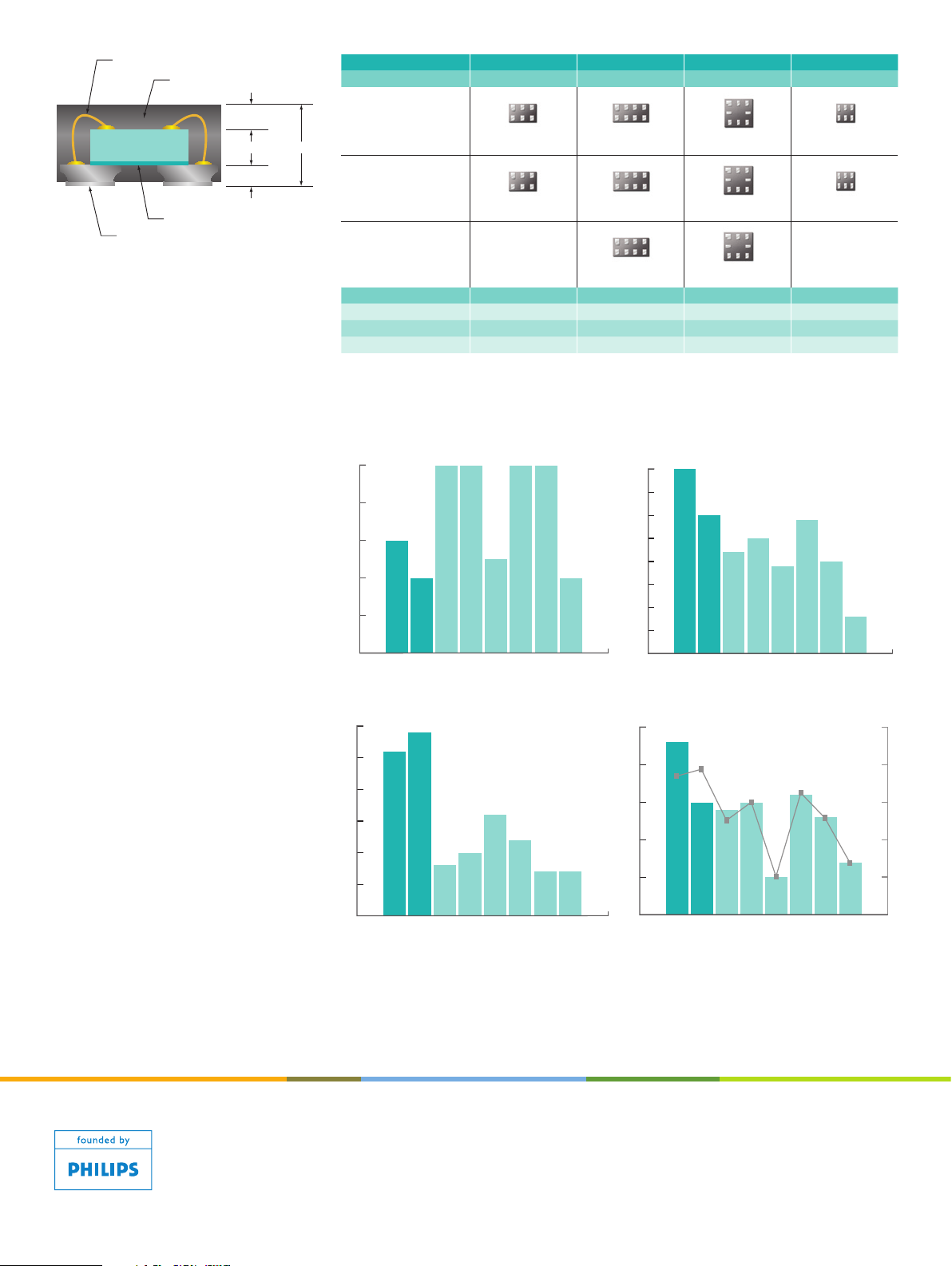
MicroPak and MicroPak II packages are the world’s smallest packages for single-, dual-, and
triple-gate logic. They are 65% - 74% smaller than their PicoGate equivalents and offer a larger
pad size that provides a more rugged and reliable bond between the device and the PC board.
Key features
4 Smallest package, more space for
added functionality
4 Leadless format eliminates assembly
problems
4 Pb-free and RoHS compliant
4 Temperature range: -40 to +125 °C
Applications
4 Mobile phones and PDAs
4 Laptop computers and high-density
boards
4 Digital still cameras and MP3 players
4 Portable/handheld test and
measurement and consumer
equipment
Ideally suited for portable applications,
where board space is always a concern,
MicroPak and MicroPak II packages
create a smaller, slimmer design and
frees up space for added functionality.
The form factor is similar to that of
popular passive components and a
variety of popular functions are available,
including gates, flip-flops, single and
dual buffers, inverters, configurable
gates and translators.
MicroPak and MicroPak II use the same
silicon as found in the HC/T, AHC/T,
LVC, and AUP PicoGate families, so
the electrical performance is highly
predictable. For easy upgrades, the
MicroPak and MicroPak II packages also
maintain the industry-standard pad pitch
of 0.5 mm and 0.35mm.
The six-pin MicroPak (GM) package
measures only 1.0 x 1.45 x 0.5 mm, so
they are 65% smaller than PicoGate
equivalents housed in SOT363 (SC-88) or
GW packages. The eight-pin packages
deliver similar space savings.
The six-pin MicroPakII is 33% smaller
than the MicroPak measuring only 1.0 x
1.0 mm and is 75% smaller than PicoGate
SOT353/363 package.
The MicroPak package can be used
as drop-in replacements for BGA and
Wafer-level Chip Scale Package (WCSP)
devices, since the layout requirements
for alignment and geometry are the
same for all of them.
MicroPak and MicroPak II are more
rugged than WCSP. Encapsulation
protects the die from breaks, scratches,
Page 2

0.15 mm
0.22 mm < 0.5 mm
0.127 mm
Wire bond (gold wire)
Mold compound
Matt tin
Die-attach material
Die
Package suffix
0.0
0.5
1.0
1.5
2.0
2.5
MicroPak
MicroPak II
Leadless
Leadless
Leaded
Leaded
Leadless
Leaded
Leaded
Leaded
SOT666 SOT553 fSv
SOT665
WCSP
FE
mm
2
Footprint (area)
0.00
0.05
0.10
0.15
0.20
0.25
0.30
0.35
0.40
MicroPak
MicroPak II
Leadless
Leadless
Leaded
Leaded
Leadless
Leaded
Leaded
Leaded
SOT666 SOT553 fSv
SOT665
WCSP
FE
mm
2
Contact area (total)
0
5
10
15
20
25
30
MicroPak
MicroPak II
Leadless
Leadless
Leaded
Leaded
Leadless
Leaded
Leaded
Leaded
SOT666 SOT553 fSv
SOT665
WCSP
FE
(%)
Contact — footprint ratio
0
5
10
15
20
25
MicroPak
MicroPak II
Leadless
Leadless
Leaded
Leaded
Leadless
Leaded
Leaded
Leaded
SOT666 SOT553 fSv
SOT665
WCSP
FE
Pull force
Dislocation force (Newtons)
0
5
10
15
20
25
Shear force
Single gate
Dual gate
Triple gate
GM GT GM GF
6-Pin 8-Pin 8-Pin 6-Pin
SOT886 SOT883 SOT902 SOT891
SOT886 SOT883 SOT902 SOT891
MicroPak cross sectional view
and environmental conditions. The
pads are 40% larger than on a WCSP
device, and 30% larger than on a leaded
package of the same footprint, so there’s
more contact area with the circuit board.
MicroPak and MicroPak II have no
leads, so they eliminate the assembly
problems associated with bent and nonplanar leads. They’re also Pb-free and
RoHS compliant, so they meet higher
standards for environmental friendliness.
The NXP MicroPak and MicroPak II
packages evolved from the company’s
Micro Carrier Device (MCD), a discrete
MOS leadless package built using a
quad flat non-leaded technology. MCD
is the world’s smallest package for single
diodes and transistors and improves RF
performance by reducing the parasitic
capacitance between the die and its
package.
SOT883 SOT902
6-Pin 8-Pin 8-Pin 6-Pin
Width (mm) 1.00 1.00 1.60 1.00
Length (mm) 1.45 1.95 1.60 1.00
Pitch (mm) 0.50 0.50 0.50 0.35
MicroPak package outline (5-pin functions use SOT886-1, pin 5 is NC).
For more information about MicroPak
and MicroPak II, please visit
www.nxp.com/logic.
MicroPak™ is a trademark of
Fairchild Semiconductors
www.nxp.com
© 2006 NXP N .V.
All r ights reserved. Reproduc tion i n whol e or in pa rt is pro hibited wi thout the prior writ ten conse nt of the copyri ght ow ner. The
inform ation presente d in thi s do cument do es n ot form part of any qu otatio n or contrac t, is believed to be accura te and reliab le and
may be change d witho ut notice. N o liabil ity will be accepted by the pub lisher for a ny conseque nce of i ts use. Publ ication the reof
does no t convey nor i mply any licens e under patent- or o ther ind ustri al or intel lectual pro pert y rights.
MicroPak offers the largest total contact area, so it provides the greatest mechanical strength
Date of re lease: De cember 2006
Docum ent orde r number : 9397 750 15771
Printe d in the USA
 Loading...