

Page 1

MICRF506
410MHz and 450MHz ISM Band
Transceiver
General Description
The MICRF506 is a true single-chip, frequency shift keying
(FSK) transceiver intended for use in half-duplex,
bidirectional RF links. The multi-channeled FSK transceiver
is intended for UHF radio equipment in compliance with the
European Telecommunication Standard Institute (ETSI)
specification, EN300 220.
The transmitter consists of a PLL frequency synthesizer
and power amplifier. The frequency synthesizer consists of
a voltage-controlled oscillator (VCO), a crystal oscillator,
dual modulus prescaler, programmable frequency dividers,
and a phase-detector. The loop-filter is external for flexibility
and can be a simple passive circuit. The output power of
the power amplifier can be programmed to seven levels. A
lock-detect circuit detects when the PLL is in lock. In
receive mode, the PLL synthesizer generates the local
oscillator (LO) signal. The N, M, and A values that give the
LO frequency are stored in the N0, M0, and A0 registers.
The receiver is a zero intermediate frequency (IF) type
which makes channel filtering possible with low-power,
integrated low-pass filters. The receiver consists of a low
noise amplifier (LNA) that drives a quadrature mix pair. The
mixer outputs feed two identical signal channels in phase
quadrature. Each channel includes a pre-amplifier, a third
order Sallen-Key RC low-pass filter that protects the
following switched-capacitor filter from strong adjacent
channel signals, and a limiter. The main channel filter is a
switched-capacitor implementation of a six-pole elliptic low
pass filter. The cut-off frequency of the Sallen-Key RC filter
can be programmed to four different frequencies: 100kHz,
150kHz, 230kHz, and 340kHz. The I and Q channel
outputs are demodulated and produce a digital data output.
The demodulator detects the relative phase of the I and the
Q channel signal. If the I channel signal lags behind the Q
channel, the FSK tone frequency is above the LO
frequency (data '1'). If the I channel leads the Q channel,
the FSK tone is below the LO frequency (data '0'). The
output of the receiver is available on the DataIXO pin. A
receive signal strength indicator (RSSI) circuit indicates the
received signal level. All support documentation can be
found on Micrel’s web site at www.micrel.com.
RadioWire®
Features
• True single chip transceiver
• Digital bit synchronizer
• Received signal strength indicator (RSSI)
• RX and TX power management
• Power down function
• Reference crystal tuning capabilities
• Frequency error estimator
• Baseband shaping
• Three-wire programmable serial interface
• Register read back function
Applications
• Telemetry
• Remote metering
• Wireless controller
• Remote data repeater
• Remote control systems
• Wireless modem
• Wireless security system
July 2006
1
M9999-092904
+1 408-944-0800
Page 2

Micrel MICRF506BML/YML
General Description....................................................................................................................................................1
Features......................................................................................................................................................................1
Applications ................................................................................................................................................................1
RadioWire® RF Selection Guide................................................................................................................................4
Ordering Information...................................................................................................................................................4
Block Diagram ............................................................................................................................................................4
Pin Configuration ........................................................................................................................................................5
Pin Description............................................................................................................................................................5
Absolute Maximum Ratings
Operating Ratings
(2)
....................................................................................................................................................6
Electrical Characteristics
(1)
.....................................................................................................................................6
(4)
.........................................................................................................................................6
Programming ..............................................................................................................................................................9
Writing to the control registers in MICRF506 ...........................................................................................................10
Writing to a Single Register ......................................................................................................................................10
Writing to All Registers .............................................................................................................................................11
Writing to n Registers having Incremental Addresses..............................................................................................11
Writing to n Registers having Non-Incremental Addresses......................................................................................12
Reading from the control registers in MICRF506.....................................................................................................12
Programming interface timing...................................................................................................................................12
Power on Reset ........................................................................................................................................................13
Programming summary ............................................................................................................................................14
Frequency Synthesizer.............................................................................................................................................15
Crystal Oscillator (XCO)........................................................................................................................................16
VCO ......................................................................................................................................................................17
Charge Pump........................................................................................................................................................18
PLL Filter...............................................................................................................................................................18
Lock Detect ...........................................................................................................................................................18
Modes of Operation ..............................................................................................................................................18
Transceiver Sync/Non-Synchronous Mode..............................................................................................................19
Data Interface ...........................................................................................................................................................19
Receiver....................................................................................................................................................................20
Front End ..............................................................................................................................................................20
Sallen-Key Filters..................................................................................................................................................20
Switched Capacitor Filter ......................................................................................................................................21
RSSI......................................................................................................................................................................21
FEE .......................................................................................................................................................................22
Bit Synchronizer....................................................................................................................................................23
Transmitter................................................................................................................................................................24
Power Amplifier.....................................................................................................................................................24
Modulator ..............................................................................................................................................................26
Using the XCO-tune Bits ..........................................................................................................................................28
Typical Application....................................................................................................................................................30
July 2006
2
M9999-092904
+1 408-944-0800
Page 3

Micrel MICRF506BML/YML
MICRF506BML/YML Land pattern ...........................................................................................................................31
Layout Considerations..............................................................................................................................................32
Package Information MICRF506BML.......................................................................................................................33
Package Information MICRF506YML.......................................................................................................................34
Overview of programming bit....................................................................................................................................35
Table 1: Detailed description of programming bit.....................................................................................................35
Table 2: Main Mode bit .............................................................................................................................................40
Table 3: Synchronizer mode bit................................................................................................................................40
Table 4: Modulation bit .............................................................................................................................................40
Table 5: Prefilter bit...................................................................................................................................................40
Table 6: Power amplifier bit ......................................................................................................................................41
Table 7:Generation of Bitrate_clk, BitSync_clk and Mod_clk...................................................................................41
Table 8: Test signals.................................................................................................................................................41
Table 10: Frequency Error Estimation control bit .....................................................................................................42
Table 11: Frequency Error Estimation control bit, cont. ...........................................................................................42
July 2006
3
M9999-092904
+1 408-944-0800
Page 4
Micrel MICRF506BML/YML
RadioWire® RF Selection Guide
Device Frequency Range
Maximum
Data Rate
Receive
Supply
Voltage
Transmit
Modulation
Type
Package
MICRF500 700MHz – 1.1GHz 128k Baud 12mA 2.5 to 3.4V 50mA FSK LQFP-44
MICRF501 300MHz – 440MHz 128k Baud 8mA 2.5 to 3.4V 45mA FSK LQFP-44
MICRF505 850MHz – 950MHz 200k Baud 13mA 2.0 to 2.5V 28mA FSK MLF™-32
MICRF506 410MHz – 450MHz 200k Baud 12mA 2.0 to 2.5V 21.5mA FSK MLF™-32
MICRF405 290-980MHz 200k Baud NA 2.0-3.6V 18mA FSK/ASK MLF™-24
Ordering Information
Part Number Junction Temp. Range
MICRF506YML TR –40° to +85°C Lead free 32-Pin MLF
MICRF506BML TR –40° to +85°C 32-Pin MLF
(1)
Package
TM
TM
____________________________________________________________________________________________________
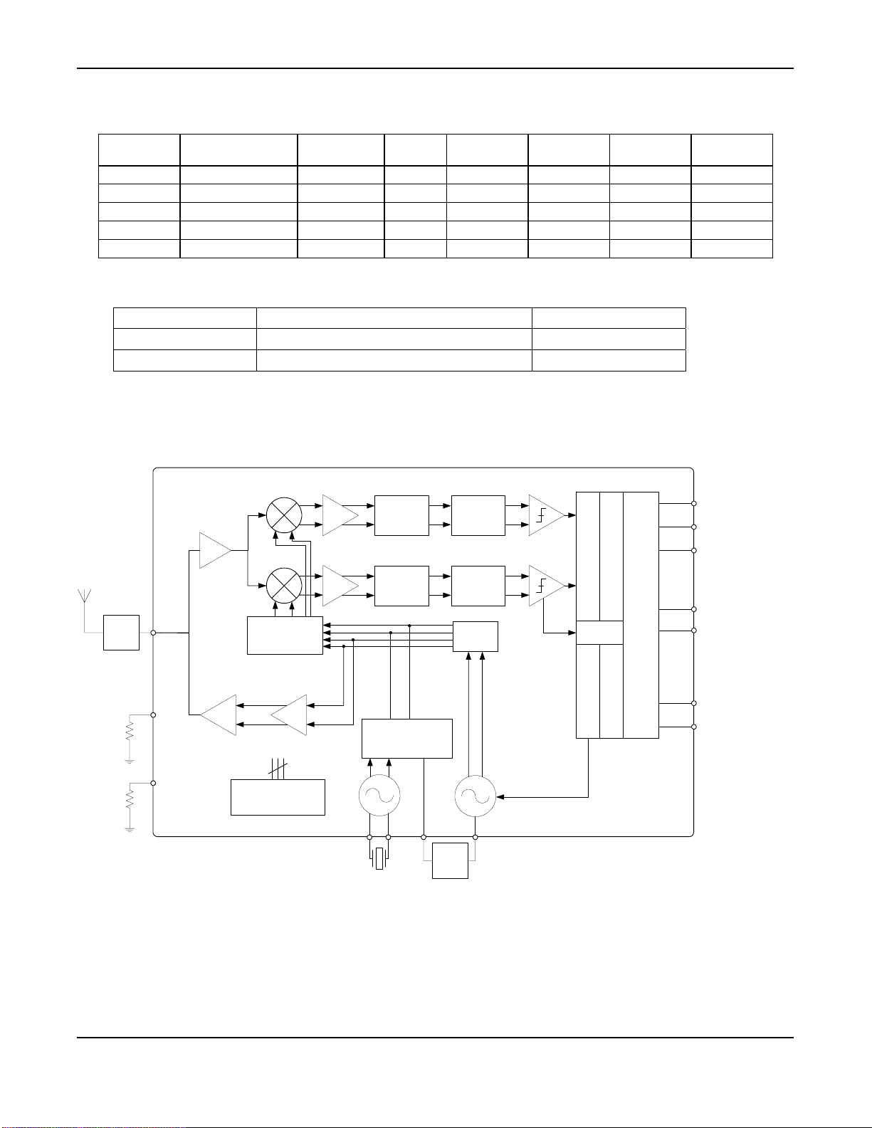
Block Diagram
SCLK
IO
CS
LNA
IFAMP
Sallen-key
Main
filter
Clock recovery
Demodulator
LC Filter
ANT
CIBIAS
PTATBIAS
IFAMP
LO-Buffer
PA
PA-buffer
Bias
XTALIN
XCO
Sallen-key
Frequency
Synthesiser
CPOUT
Loop
filter
Main
filter
DIV 4
VCO
Control logic
DATAIXO
RSSI
Modulator
Deviation control
VARINXTALOUT
DATACLK
RSSI
LD
July 2006
4
M9999-092904
+1 408-944-0800
Page 5
Micrel MICRF506BML/YML
P
T
K
D
Q
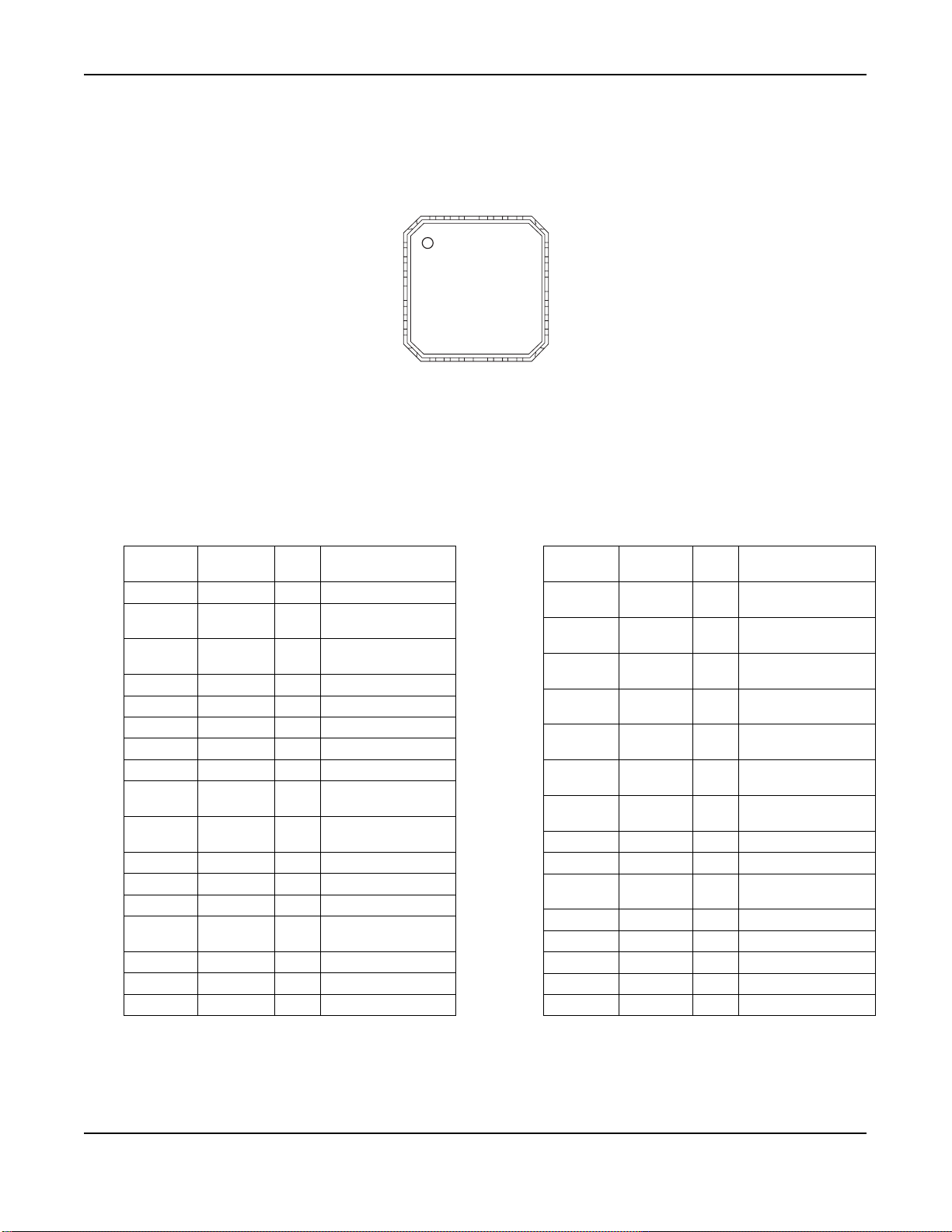
Pin Configuration
GND
VARIN
VCOGN
RFGND
TATBIAS
RFVDD
RFGND
ANT
RFGND
GND
NC
VCOVDDNC
32 3130 29 28 272625
1
2
3
4
5
6
7
8
9 10111213141516
IFVDD
CIBIAS
IFGND
ICHOUT
CPOUT
DIGGND
LD
RSSI
CHOUT
DIGVDD
XTALOU
24
23
XTALIN
22
CS
21
SCLK
20
IO
19
DATAIXO
DATACL
18
NC
17
NC
MICRF506BML
32-Pin MLF
TM
Pin Description
Pin
Number
1 RFGND LNA and PA ground.
2 PTATBIAS O Connection for bias
3 RFVDD LNA and PA power
4 RFGND LNA and PA ground.
5 ANT I/O Antenna In/Output.
6 RFGND LNA and PA ground.
7 RFGND LNA and PA ground.
8 NC No connect.
9 CIBIAS O Connection for bias
10 IFVDD IF/mixer power
11 IFGND IF/mixer ground.
12 ICHOUT O Test pin.
13 QCHOUT O Test pin.
14 RSSI O Received signal
15 LD O PLL lock detect.
16 NC No connect.
17 NC No connect
Pin Name Type Pin Function
resistor.
supply.
resistor.
supply.
strength indicator.
Pin
Pin Name Type Pin Function
Number
18 DATACLK O RX/TX data clock
output.
19 DATAIXO I/O RX/TX data
input/output.
20 IO I/O 3-wire interface data
in/output.
21 SCLK I 3-wire interface serial
clock.
22 CS I 3-wire interface chip
select.
23 XTALIN I Crystal oscillator
input.
24 XTALOUT O Crystal oscillator
output.
25 DIGVDD Digital power supply.
26 DIGGND Digital ground.
27 CPOUT O PLL charge pump
output.
28 GND Substrate ground.
29 VARIN I VCO varactor.
30 VCOGND VCO ground.
31 VCOVDD VCO power supply.
32 NC No connect.
July 2006
5
M9999-092904
+1 408-944-0800
Page 6
Micrel MICRF506BML/YML
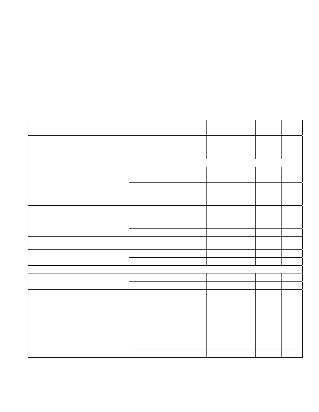
Absolute Maximum Ratings
(1)
Operating Ratings
(2)
Supply Voltage (VDD) ........................................ +2.7V
Voltage on any pin (GND = 0V). .....-0.3V to 2.7V
Storage Temperature (T
ESD Rating
(3)
....................................................... 2kV
)................ -55°C to +150°C
s
Supply voltage (VIN) ............................+2.0V to +2.5V
RF Frequencies ..........................410MHz to 450MHz
Data Rate ................................................ <200kBaud
Ambient Temperature (T
Package Thermal Resistance
MLF
TM
(θJA)........................................... 41.7°C/W
)................ –40°C to +85°C
A
Electrical Characteristics
(4)
fRF = 433MHz. Data-rate = 125kbps, Modulation type = closed-loop VCO modulation, VDD = 2.5V; TA = 25°C, bold
values indicate –40°C
Symbol Parameter Condition Min Typ Max Units
RF Frequency Operating Range
Power Supply
Power Down Current 0.3
Standby Current 280
VCO and PLL Section
Reference Frequency
3kHz bandwidth
PLL Lock Time
20kHz bandwidth
Switch Time
3kHz loop bandwidth
Transmit Section
July 2006
Crystal Oscillator Start-Up Time
Charge Pump Current
Output Power
Output Power Tolerance
Tx Current Consumption
Binary FSK Frequency
Separation
Data Rate
< TA < +85°C, unless noted.
(5)
(5)
(5)
(5)
(5)
433.75MHz to 434.25MHz 0.7
430MHz to 440MHz 1.3
433.75MHz to 434.25MHz 0.3 ms
Rx – Tx 1.0
Tx – Rx 1.0
Standby Rx 1.0
Standby Tx 1.0 ms
16MHz, 9pF load, 5.6pF loading
capacitors
VCP
VCP
R
R
Over temperature range 1 dB
Over power supply range 3 dB
R
R
R
Birate = 200kbps
VCO modulation
Divider modulation
= 1.1V, CP_HI = 0
OUT
= 1.1V, CP_HI = 1
OUT
= 50Ω, Pa2-0-111
LOAD
= 50Ω, Pa2-0-001
LOAD
= 50Ω, Pa2-0-111
LOAD
= 50Ω, Pa2-0-001
LOAD
= 50Ω, Pa2-0-000
LOAD
6
410
2.0
4 40
450
2.5
3
1.3
2
1.4
2.5
3
MHz
V
µA
µA
MHz
ms PLL Lock Time
ms
ms
ms
ms
1.0 ms
100
420
125
500
170
680
µA
µA
11 dBm
-7 dBm
21.5 mA
10.5 mA
8.0 mA
20 500
20 200
20
kHz
kbps
kbps
M9999-092904
+1 408-944-0800
Page 7
Micrel MICRF506BML/YML
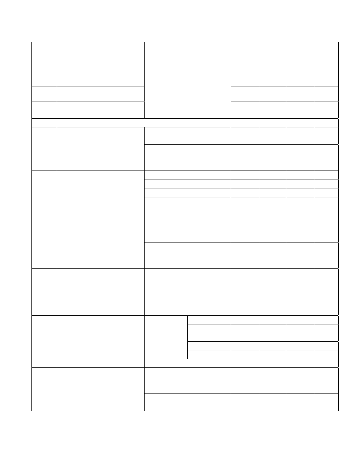
Symbol Parameter Condition Min Typ Max Units
Occupied bandwidth
(5)
38.4kbps, β = 2, 20dBc
125kbps, β = 2, 20dBc
200kbps, β = 2, 20dBc
Harmonics 434MHz
Spurious Emission in Restricted
bands < 1GHz
Spurious Emission < 1GHz
Spurious Emission > 1GHz
(5)
(5)
(5)
(5)
ETSI EN300 220
(Using antenna matching network)
Receive Section
Rx Current Consumption
All functions turned on 12 mA
LNA bypass 10.3 mA
Switch cap filter bypass with LNA 9.8 mA
Bypass of Switch cap and LNA
Rx Current Consumption Variation Over temperature 3 mA
2.4kbps, β = 16, BER 10
4.8kbps, β = 16, BER 10
19.2kbps, β = 4, BER 10
Receiver Sensitivity
38.4kbps, β = 4, BER 10
76.8kbps, β = 2, BER 10
125kbps, β = 2, BER 10
200kbps, β = 2, BER 10
Receiver Maximum Input Power
Receiver Sensitivity Tolerance
125kbps, 125kHz deviation +12 dBm
20kbps, 40kHz deviation +2 dBm
Over temperature 4 dB
Over power supply range 1 dB
-3
-3
-3
-3
-3
-3
-3
Receiver Bandwidth 50 350 kHz
Co-Channel Rejection
Adjacent Channel Rejection
19.2 kbps, β = 6, SC=133 kHz
500kHz spacing, 19.2kbps, Main
filter cut off frequency 133kHz
1MHz ,19.2kbps, Main filter cut off
frequency 133kHz
Offset ±1MHz
Offset ±2MHz
Offset ±5MHz
Offset ±10MHz
Offset ±30MHz
Desired signal:
Blocking
19.2 kbps, β =6,
3dB above sens,
SC=133 kHz
1dB Compression
Input IP3 2 tones with 1MHz separation -25 dBm
LO Leakage -90 dBm
Spurious Emission
Input Impedance
(5)
(5)
<1GHz, EN 300 220 -57 dBm
>1GHz, EN 300 220 -47 dBm
50
140 kHz
550 kHz
800 kHz
-36
-54
-36
-30
dBm
dBm
dBm
dBm
8.0 mA
-113 dBm
-111 dBm
-106 dBm
-104 dBm
-101 dBm
-100 dBm
-97 dBm
-8 dB
48 dB
56 dB
61 dB
58 dB
46 dB
62 dB
75 dB
-34 dBm
Ω
July 2006
7
M9999-092904
+1 408-944-0800
Page 8
Micrel MICRF506BML/YML
Symbol Parameter Condition Min Typ Max Units
RSSI Dynamic Range 50 dB
RSSI Output Range
Digital Inputs/Outputs
V
IH
V
IL
Clock/Data Frequency
Clock/Data Duty Cycle
Notes:
1. Exceeding the absolute maximum rating may damage the device.
2. The device is not guaranteed to function outside its operating rating.
3. Devices are ESD sensitive. Handling precautions recommended. Human body model, 1.5k in series with 100pF.
4. Specification for packaged product only.
5. Guaranteed by design.
Logic Input High 0.7V
Logic Input Low 0 0.3V
(5)
(5)
Pin = -110dBm 0.9 V
Pin = -60dBm 2 V
DD
VDDV
DD
V
10 MHz
45 55 %
July 2006
8
M9999-092904
+1 408-944-0800
Page 9
Micrel MICRF506BML/YML
Programming
General
The MICRF506 functions are enabled through a
number of programming bits. The programming bits
are organized as a set of addressable control
registers, each register holding 8 bits.
There are 23 control registers in total in the
MICRF506, and they have addresses ranging from 0
to 22. The user can read all the control registers.
The user can write to the first 22 registers (0 to 21);
the register 22 is a read-only register.
All control registers hold 8 bits and all 8 bits must be
written to when accessing a control register, or they
will be read. Some of the registers do not utilize all 8
bits. The value of an unused bit is “don’t care.”
The control register with address 0 is referred to as
ControlRegister0, the control register with address 1
is ControlRegister1 and so on. A summary of the
control registers is given in the table below. In
addition to the unused bits (marked with”-“) there are
a number of mandatory bits (marked with “0” or “1”).
Always maintain these as shown in the table.
Adr Data
A6…A0 D7 D6 D5 D4 D3 D2 D1 D0
0000000 LNA_by PA2 PA1 PA0 Sync_en Mode1 Mode0 Load_en
0000001 Modulation1 Modulation0 ‘0’ ‘0’ RSSI_en LD_en PF_FC1 PF_FC0
0000010 CP_HI SC_by ‘0’ PA_By OUTS3 OUTS2 OUTS1 OUTS0
0000011 ‘1’ ‘1’ ‘0’ VCO_IB2 VCO_IB1 VCO_IB0 VCO_freq1 VCO_freq0
0000100 Mod_F2 Mod_F1 Mod_F0 Mod_I4 Mod_I3 Mod_I2 Mod_I1 Mod_I0
0000101 - - ‘0’ ‘1’ Mod_A3 Mod_A2 Mod_A1 Mod_A0
0000110 - Mod_clkS2 Mod_clkS1 Mod_clkS0 BitSync_clkS2 BitSync_clkS1 BitSync_clkS0 BitRate_clkS2
0000111 BitRate_clkS1 BitRate_clkS0 RefClk_K5 RefClk_K4 RefClk_K3 RefClk_K2 RefClk_K1 RefClk_K0
0001000 ‘1’ ‘1’ ‘0’ ScClk4 ScClk3 ScClk2 ScClk1 ScClk0
0001001 ‘0’ ‘0’ ‘1’ XCOtune4 XCOtune3 XCOtune2 XCOtune1 XCOtune0
0001010 - - A0_5 A0_4 A0_3 A0_2 A0_1 A0_0
0001011 - - - - N0_11 N0_10 N0_9 N0_8
0001100 N0_7 N0_6 N0_5 N0_4 N0_3 N0_2 N0_1 N0_0
0001101 - - - - M0_11 M0_10 M0_9 M0_8
0001110 M0_7 M0_6 M0_5 M0_4 M0_3 M0_2 M0_1 M0_0
0001111 - - A1_5 A1_4 A1_3 A1_2 A1_1 A1_0
0010000 - - - - N1_11 N1_10 N1_9 N1_8
0010001 N1_7 N1_6 N1_5 N1_4 N1_3 N1_2 N1_1 N1_0
0010010 - - - - M1_11 M1_10 M1_9 M1_8
0010011 M1_7 M1_6 M1_5 M1_4 M1_3 M1_2 M1_1 M1_0
0010100 ‘1’ ‘0’ ‘1’ ‘0’ ‘0’ ‘0’ ‘1’ ‘1’
0010101 - - - - FEEC_3 FEEC_2 FEEC_1 FEEC_0
0010110 FEE_7 FEE_6 FEE_5 FEE_4 FEE_3 FEE_2 FEE_1 FEE_0
Names of programming bits, unused bits (“-“) and mandatory bits (“1” or “0”) are shown. Change of mandatory bits may cause malfunction.
The control registers in MICRF506 are accessed
through a 3-wire interface; clock, data and chip
select. These lines are referred to as SCLK, IO, and
CS, respectively. This 3-wire interface is dedicated
to control register access and is referred to as the
control interface. Received data (via RF) and data to
transmit (via RF) are handled by the DataIXO and
DataClk (if enabled) lines; this is referred to as the
data interface.
The SCLK line is applied externally; access to the
control registers are carried out at a rate determined
by the user. The MICRF506 will ignore transitions on
the SCLK line if the CS line is inactive. The
MICRF506 can be put on a bus, sharing clock and
data lines with other devices.
All control registers should be written to after a
battery reset. During operation, it is sufficient to write
to one register only. The MICRF506 will
automatically enter power down mode after a battery
reset.
July 2006
Table 1. Control Registers in MICRF506
9
M9999-092904
+1 408-944-0800
Page 10
Micrel MICRF506BML/YML
C
Writing to the control registers in MICRF506
Writing: A number of octets are entered into
MICRF506 followed by a load-signal to activate the
new setting. Making these events is referred to as a
“write sequence.” It is possible to update all, 1, or n
control registers in a write sequence. The address to
write to (or the first address to write to) can be any
valid address (0-21). The IO line is always an input
to the MICRF506 (output from user) when writing.
What to write:
• The address of the control register to write
to (or if more than 1 control register should
be written to, the address of the 1
st
control
register to write to).
• A bit to enable reading or writing of the
control registers. This bit is called the R/W
bit.
• The values to write into the control
register(s).
What to write:
Field Comments
Address: A 7-bit field, ranging from 0 to 21. MSB is
written first.
R/W bit: A 1-bit field, = “0” for writing
Values: A number of octets (1-22 octets). MSB in
every octet is written first. The first octet is
written to the control register with the
specified address (=”Address”). The next
octet (if there is one) is written to the control
register with address = “Address + 1” and so
on.
Table 2.
How to write:
Bring CS active to active to start a write sequence.
The two different ways to “program the chip” are:
• Write to a number of control registers (0-22)
when the registers have incremental
addresses (write to 1, all or n registers)
• Write to a number of control registers when
the registers have non-incremental
addresses.
Writing to a Single Register
Writing to a control register with address “A6. A5,
…A0” is described here. During operation, writing to
1 register is sufficient to change the way the
transceiver works. Typical example: Change from
receive mode to power-down.
What to write:
Field Comments
Address: 7 bit = A6, A5, …A0 (A6 = msb. A0 = lsb)
R/W bit: “0” for writing
Values: 8 bits = D7, D6, …D0 (D7 = msb, D0 = lsb)
Table 3.
“Address” and “R/W bit” together make 1 octet.
In addition, 1 octet with programming bits is entered. In
total, 2 octets are clocked into the MICRF506.
How to write:
• Bring CS high
• Use SCLK and IO to clock in the 2 octets
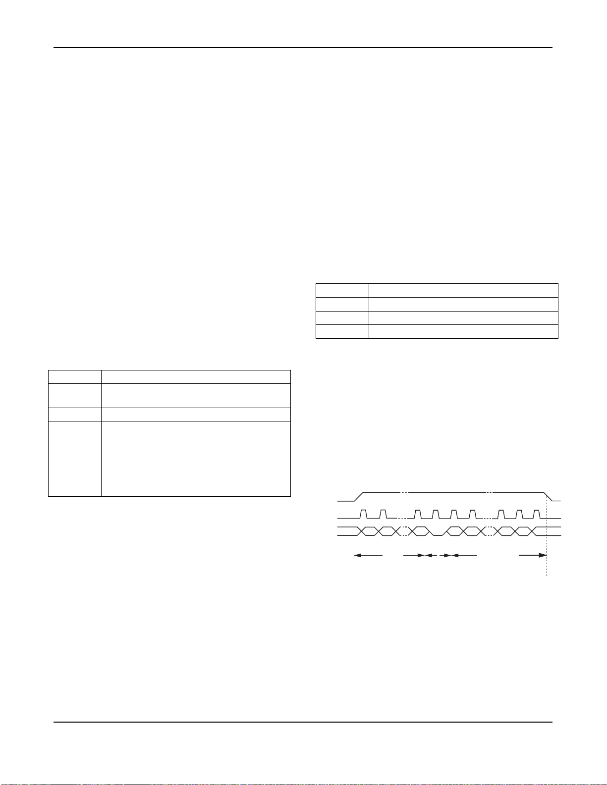
• Bring CS low
S
SCLK
IO
A6 A5 A0
D7 D6 D2
RW
D1 D0
The active state of the CS line is “high.” Use the
SCLK/IO serial interface to clock “Address” and
“R/W” bit and “Values” into the MICRF506.
Address of register i RW Data to write into register i
Internal load pulse made here
MICRF506 will sample the IO line at negative edges
of SCLK. Make sure to change the state of the IO
line before the negative edge. Refer to figures
below.
Bring CS inactive to make an internal load-signal
and complete the write-sequence. Note: there is an
exception to this point. If the programming bit called
Figure 1.
In Figure 1, IO is changed at positive edges of SCLK. The
MICRF506 samples the IO line at negative edges. The
value of the R/W bits is always “0” for writing.
“load_en” (bit0 in ControlRegister0) is “0”, then no
load pulse is generated.
July 2006
10
M9999-092904
+1 408-944-0800
Page 11
Micrel MICRF506BML/YML
C
Writing to All Registers
After a power-on, all writable registers should be
written. This is described here.
Writing to all register can be done at any time. To
get the simplest firmware, always write to all
registers. The price to pay for the simplicity is
increased write-time, which leads to increased time
to change the way the MICRF506 works.
What to write
Field Comments
Address: ‘000000’ (address of the first register to write
to, which is 0)
R/W bit: “0” for writing
Values: 1st Octet: wanted values for
ControlRegister0. 2
for ControlRegister1 and so on for all of the
octets. So the 22
nd
Octet: wanted values
nd
octet wants values for
ControlRegister21. Refer to the specific
sections of this document for actual values.
Table 4.
“Address” and “R/W bit” together make 1 octet.
In addition, 22 octets with programming bits are entered.
In total, 23 octets are clocked into the MICRF506.
How to write:
• Bring CS high
• Use SCLK and IO to clock in the 23 octets
• Bring CS low
Refer to the figure in the next section, “Writing to n
registers having incremental addresses”.
Writing to n Registers having Incremental
Addresses
In addition to entering all bytes, it is also possible to
enter a set of n bytes, starting from address i = “A6,
A5, … A0”. Typical example: Clock in a new set of
frequency dividers (i.e. change the RF frequency).
“Incremental addresses”. Registers to be written are
located in i, i+1, i+2.
What to write
Field Comments
Address: 7 bit = A6, A5, …A0 (A6 = msb. A0 = lsb)
(address of first byte to write to)
R/W bit: “0” for writing
Values: n* 8 bits =
D7, D6, …D0 (D7 = msb, D0 = lsb) (written
to control reg. with address ”i”)
D7, D6, …D0 (D7 = msb, D0 = lsb) (written
to control reg. with address ”i+1”)
D7, D6, …D0 (D7 = msb, D0 = lsb) (written
to control reg. with address ”i+n-1”)
Table 5.
“Address” and “R/W bit” together make 1 octet.
In addition, n octets with programming bits are entered.
Totally, 1 +n octets are clocked into the MICRF506.
How to write:
• Bring CS high
• Use SCLK and IO to clock in the 1 + n
octets
• Bring CS low
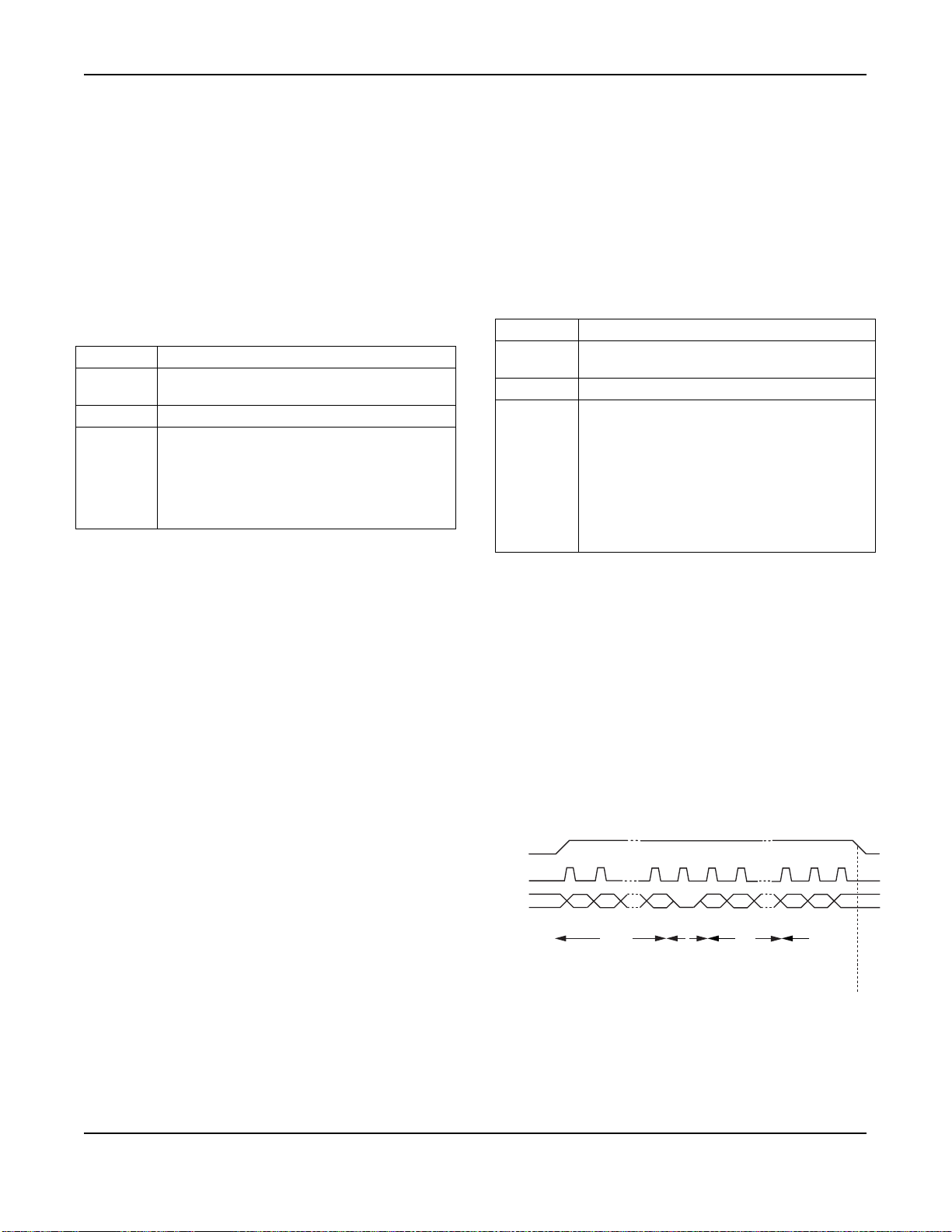
In Figure 1, IO is changed at positive edges of SCLK. The
MICRF506 samples the IO line at negative edges. The
value of the R/W bits is always “0” for writing.
S
SCLK
IO
A6 A5 A0
Address of first RW
register to write to,
register i
D7 D6 D2
RW
Data to write
into register i
Internal load pulse made here
D1 D0
Data to write
into register i+1
Figure 2.
July 2006
11
M9999-092904
+1 408-944-0800
Page 12
Micrel MICRF506BML/YML
S
I
I
C
S
I
D
Tscl
Twrite
TreadThigh
TperTcsr
traise
Writing to n Registers having Non-Incremental
Addresses
Registers with non-incremental addresses can be
written to in one write-sequence as well. Example of
non-incremental addresses: “0,1,3”. However, this
requires more overhead, and the user should
consider the possibility to make a “continuous”
update, for example, by writing to “0,1,2,3” (writing
the present value of “2” into “2”). The simplest
firmware is achieved by always writing to all
registers. Refer to previous sections.
This write-sequence is divided into several subparts:
• Disable the generation of load-signals by
clearing bit “load_en” (bit0 in
ControlRegister0)
• Repeat for each group of register having
incremental addresses:
o Bring CS active
o Enter first address for this group,
R/W bit and values
o Bring CS inactive
o Finally, enable and make a load-
signal by setting “load_en”
Refer to the previous sections for how to write to 1 or
n (with incremental addresses) registers in the
MICRF506.
Reading from the control registers in MICRF506
The “read-sequence” is:
1. Enter address and R/W bit
2. Change direction of IO line
3. Read out a number of octets and change IO
direction back again.
It is possible to read all, 1 or n registers. The
address to read from (or the first address to read
from) can be any valid address (0-22). Reading is
not destructive, i.e. values are not changed. The IO
line is output from the MICRF506 (input to user) for a
part of the read-sequence. Refer to procedure
description below.
Reading n registers from MICRF506
CS
SCLK
D0
imple time
O Input
O Output
IO
A6 A5 A0
Address of register i RWData read from reg. i
RW
D7 D6
Figure 3.
In the figure, 1 register is read. The address is A6,
A5, … A0. A6 = msb. The data read out is D7, D6,
…D0. The value of the R/W bit is always “1” for
reading.
SCLK and IO together form a serial interface. SCLK
is applied externally for reading as well as for writing.
• Bring CS active
• Enter address to read from (or the first
address to read from) (7 bits) and
• The R/W bit = 1 to enable reading
• Make the IO line an input to the user (set pin
in tristate)
• Read n octets. The first rising edge of SCLK
will set the IO as an output from the
MICRF506. MICRF will change the IO line at
positive edges. The user should read the IO
line at the negative edges.
• Make the IO line an output from the user
again.
Programming interface timing
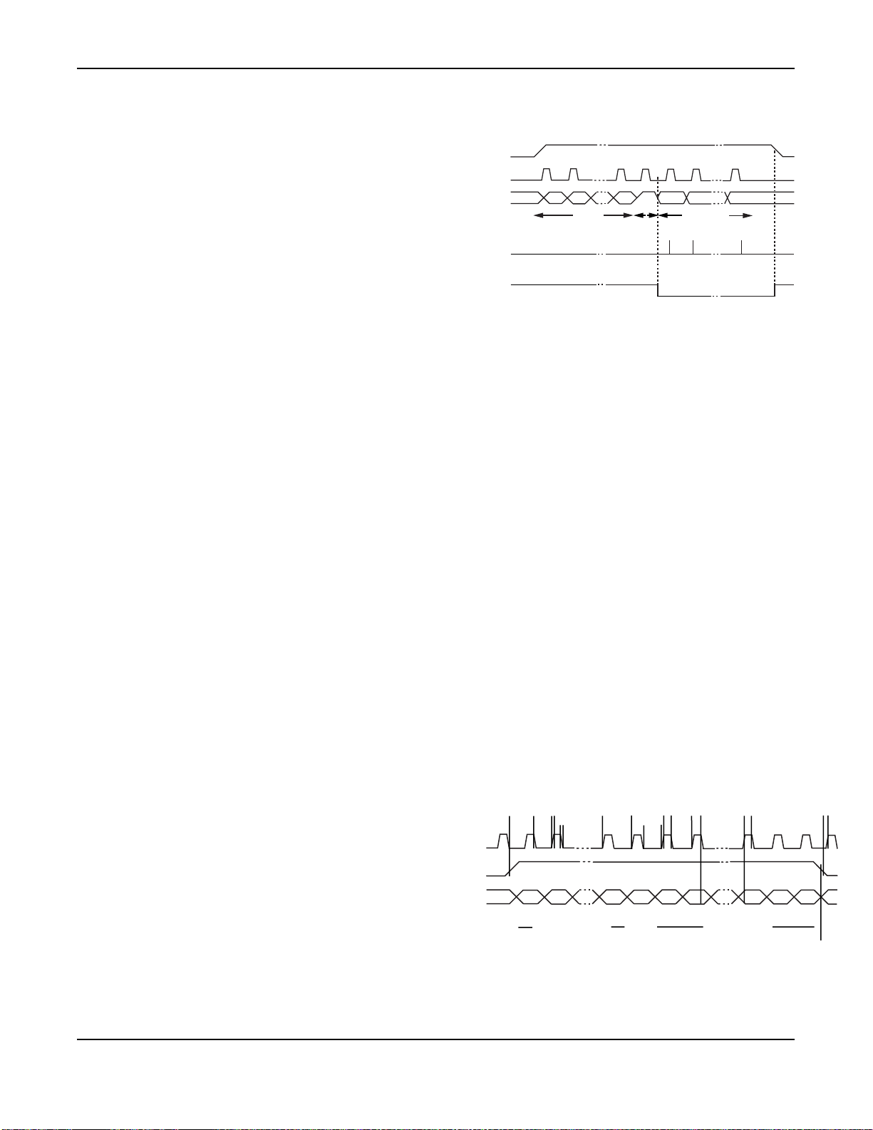
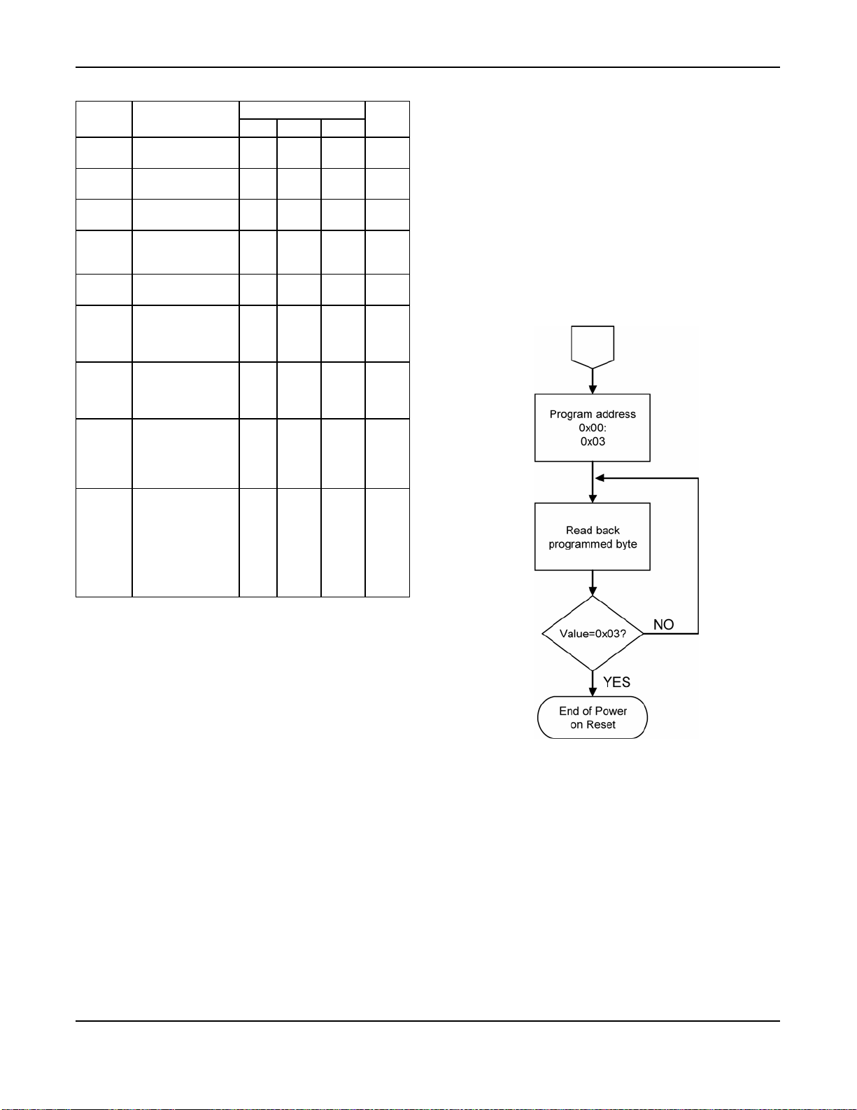
Figure 4 and Table 6 shows the timing specification for the
3-wire serial programming interface.
tfall
CLK
Tlow
A read-sequence is described for reading n
registers, where n is number 1-23.
S
O
A6 A5 A0
D7 D6 D2
RW
D1 D0
Address Register Data Register
LOA
July 2006
Figure 4.
12
M9999-092904
+1 408-944-0800
Page 13
Micrel MICRF506BML/YML
Symbol Parameter
Tper Min. period of
SCLK
Thigh Min. high time of
SCLK
Tlow Min. low time of
SCLK
tfall Max. time of
falling edge of
SCLK
trise Max. time of rising
edge of SCLK
Tcsr Max. time of rising
edge of CS to
falling edge of
SCLK
Tcsf Min. delay from
rising edge of CS
to rising edge of
SCLK
Twrite Min. delay from
valid IO to falling
edge of SCLK
during a write
operation
Tread Min. delay from
rising edge of
SCLK to valid IO
during a read
operation
(assuming load
capacitance of IO
is 25pF)
Values
Min. Typ. Max.
50 ns
20 ns
20 ns
1 µs
1 µs
0 ns
5 ns
0 ns
75 ns
Units
Power on Reset
When applying voltage to the MICRF506 a power
on reset state is entered. During the time period of
power on reset, the MICRF506 should be
considered to be in an unknown state and the user
should wait until completed (See Table 6). The
power on reset timing given in table 6 is covering all
conditions and should be treated as a maximum
delay time. In some application it might be beneficial
to minimize the power on reset time. In these cases
we recommend to follow below procedure:
Table 6. Timing Specification for the 3-wire
Programming Interface
July 2006
13
M9999-092904
+1 408-944-0800
Page 14

Micrel MICRF506BML/YML
Programming summary
• Use CS, SCLK, and IO to get access to the
control registers in MICRF506.
• SCLK is user-controlled.
• Write to the MICRF506 at positive edges
(MICRF506 reads at negative edges).
• Read from the MICRF506 at negative edges
(MICRF506 writes at positive edges)
• After power-on: Write to the complete set of
control registers.
• Address field is 7 bits long. Enter msb first.
• R/W bit is 1 bit long (“1” for read, “0” for
write)
• Address and R/W bit together make 1 octet
• All control registers are 8 bits long.
Enter/read msb in every octet first.
• Always write 8 bits to/read 8 bits from a
control register. This is the case for registers
with less than 8 used programming bits as
well.
• Writing: Bring CS high, write address and
R/W bit followed by the new values to fill into
the addressed control register(s) and bring
CS low for loading, i.e. activation of the new
control register values (“load_en” = 1).
• Reading: Bring CS high, write address and
R/W bit, set IO as an input, read present
contents of the addressed control
register(s), bring CS low and set IO an
output.
July 2006
14
M9999-092904
+1 408-944-0800
Page 15
Micrel MICRF506BML/YML
Frequency Synthesizer
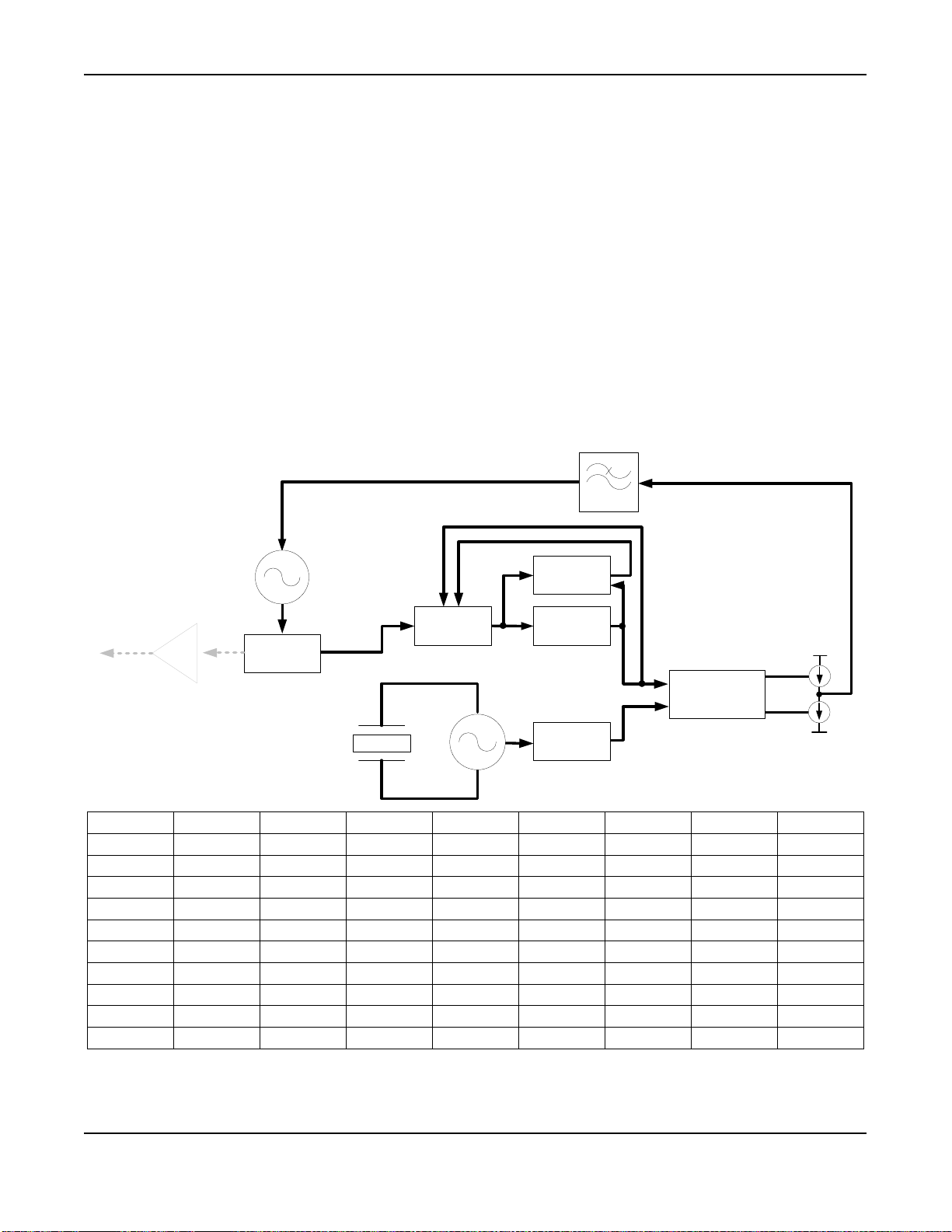
The MICRF506 frequency synthesizer consists of a voltage-controlled oscillator (VCO), a crystal oscillator, dual
modulus prescaler, programmable frequency dividers and a phase-detector. The loop-filter is external for flexibility
and can be a simple passive circuit. The phase detector compares frequencies of two signals and produces an
error signal which is proportional to the difference between the input frequencies. The error signal is used to
control a voltage-controlled oscillator (VCO) which creates an output frequency. The output frequency is fed
through a frequency divider back to the input of the phase detector, producing a feedback loop. If the output
frequency drifts, the error signal will increase, driving the frequency in the opposite direction so as to reduce the
error. Thus the output is locked to the frequency at the other input. This input is called the reference and is
derived from a crystal oscillator, which is very stable in frequency. The block diagram below shows the basic
elements and arrangement of a PLL based frequency synthesizer. The MICRF506 has a dual modulus prescaler
for increased frequency resolution. In a dual modulus prescaler the main divider is split into two parts, the main
part N and an additional divider A, where A < N. Both dividers are clocked from the output of the dual-modulus
prescaler, but only the output of the N divider is fed into the phase detector. The prescaler will first divide by 16.
Both N and A count down until A reaches zero, at which point the prescaler is switched to a division ratio 16+1. At
this point, the divider N has completed A counts. Counting continues until N reaches zero, which is an additional
N-A counts. At this point the cycle repeats.
Loop filter
1800MHz
VCO
A-Divider
Prescaler N-Divider
PA
Div/4
Charge pump
Phase
detector
XCO
M-Divider
A6…A0 D7 D6 D5 D4 D3 D2 D1 D0
0001010 - - A0_5 A0_4 A0_3 A0_2 A0_1 A0_0
0001011 - - - - N0_11 N0_10 N0_9 N0_8
0001100 N0_7 N0_6 N0_5 N0_4 N0_3 N0_2 N0_1 N0_0
0001101 - - - - M0_11 M0_10 M0_9 M0_8
0001110 M0_7 M0_6 M0_5 M0_4 M0_3 M0_2 M0_1 M0_0
0001111 - - A1_5 A1_4 A1_3 A1_2 A1_1 A1_0
0010000 - - - - N1_11 N1_10 N1_9 N1_8
0010001 N1_7 N1_6 N1_5 N1_4 N1_3 N1_2 N1_1 N1_0
0010010 - - - - M1_11 M1_10 M1_9 M1_8
0010011 M1_7 M1_6 M1_5 M1_4 M1_3 M1_2 M1_1 M1_0
July 2006
15
M9999-092904
+1 408-944-0800
Page 16
Micrel MICRF506BML/YML
X
3
N
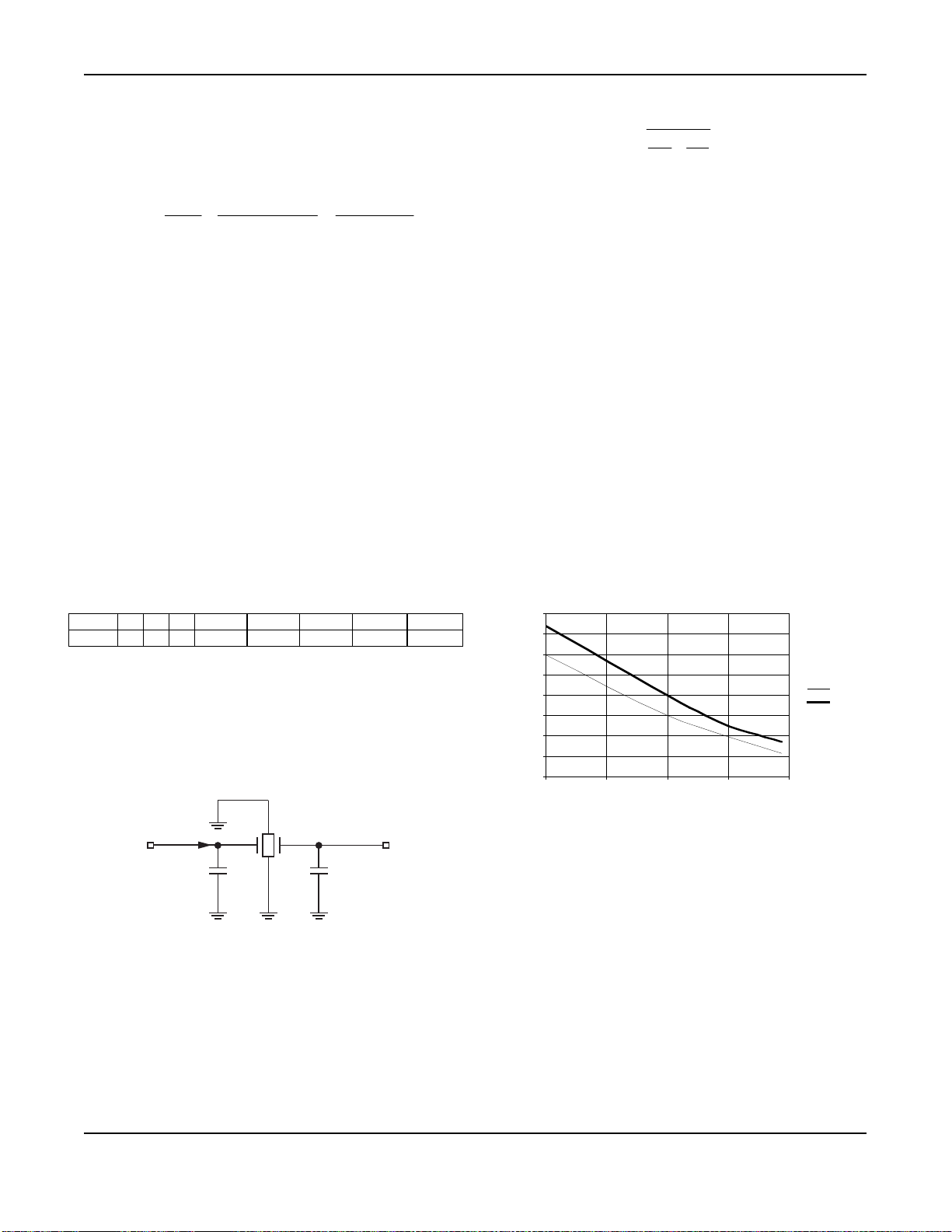
The lengths of the N, M, and A registers are 12, 12
and 6 respectively The values can be calculated
from the following formula:
f
PhD
f
M
f
VCOXCO
==
()()
=
×+×
2A N 16
RF
2f
×
A N 16
+×
M≠0
1 ≤ A < N
CL =
The parasitic capacitance is the pin input
capacitance and PCB stray capacitance. Typically,
the total parasitic capacitance is around 6pF. For
instance, for a 9pF load crystal the recommended
values of the external load capacitors are 5.6pF.
It is also possible to tune the crystal oscillator
1
1
C
10
+ C
1
+
C
11
parasitic
internally by switching in internal capacitance using
where
f
: Phase detector comparison frequency
PhD
f
: Crystal oscillator frequency
XCO
f
: Voltage controlled oscillator frequency
VCO
: RF carrier frequency
f
RF
There are two sets of each of the divide factors (i.e.
A0 and A1). If modulation by using the dividers is
selected (that is Modulation1=1, Modulation0=0), the
two sets should be programmed to give two RF
frequencies, separated by two times the specified
frequency deviation. For all other modulation
methods, and also in receive mode, the 0-set will be
used.
Crystal Oscillator (XCO)
Adr D7 D6 D5 D4 D3 D2 D1 D0
0001001 ‘0’ ‘0’ ‘1’ XCOtune4 XCOtune3 XCOtune2 XCOtune1 XCOtune0
The crystal oscillator is a very critical block. As the
crystal oscillator is a reference for the RF output
frequency and also for the LO frequency in the
receiver, very good phase and frequency stability is
required. The schematic of the crystal oscillator’s
external components for 16MHz are shown in Figure
5.
Pin 24
TALOUT
Y1
TSX-10A
Pin 2
XTALI
5 tune bits XCOtune4 – XCOtun0. When XCOtune4
– XCOtune0 = 0 no internal capacitors are
connected to the crystal pins. When XCOtune4 –
XCOtune0 = 1 all of the internal capacitors are
connected to the crystal pins. Figure 6 shows the
tuning range for two different capacitor values, 1.5pF
and no capacitors.
The crystal used is a TN4-26011 from Toyocom.
Specification: Package TSX-10A, Nominal frequency
16.000000 MHz, frequency tolerance ±10ppm,
frequency stability ±9ppm, load capacitance 9pF,
pulling sensitivity 15ppm/pF. When the external
capacitors are set to 1.5pF and the XCOtune=16,
the total capacitance will normally be ~9pF.
100,0
80,0
60,0
40,0
20,0
[ppm]
0,0
-20,0
-40,0
-60,0
0 8 16 24 32
XCO bitvalue
Figure 6. XCO Tuning
2x1.5pF
2x0pF
C10
5.6pF
Figure 5. Crystal Oscillator Circuit
The crystal should be connected between pins
XTALIN and XTALOUT (pin 23 and 24). In addition,
loading capacitors for the crystal are required. The
loading capacitor values depend on the total load
capacitance, C
, specified for the crystal. The load
L
capacitance seen between the crystal terminals
should be equal to C
for the crystal to oscillate at
L
the specified frequency.
July 2006
C11
5.6pF
The start up time is given in Table 7. As can be
seen, more capacitance will slow down the start up
time.
The start-up time of a crystal oscillator is typically
around a millisecond. Therefore, to save current
consumption, the XCO is turned on before any other
circuit block. During start-up the XCO amplitude will
eventually reach a sufficient level to trigger the Mcounter. After counting 2 M-counter output pulses
the rest of the circuit will be turned on. The current
consumption during the prestart period is
approximately 280µA.
16
M9999-092904
+1 408-944-0800
Page 17
Micrel MICRF506BML/YML
VCO frequency gain, Vdd=2.5V
380
390
400
410
420
430
440
450
460
470
480
0 0.4 0.8 1.2 1.6 2 2.4
V_varactor [V]
Freq [MHz]
11
10
01
00
XCOtune Start-up Time (µs)
0 590
1 590
2 700
4 700
8 810
16 1140
31 2050
Table 7. Typical values with C
= 1.5pF
EXT
If an external reference is used instead of a crystal,
the signal shall be applied to pin 24, XTALOUT. Due
to internal DC setting in the XCO, an AC coupling is
recommended to be used between the external
reference and the XTALOUT-pin.
VCO
A6..A0 D7 D6 D5 D4 D3 D2 D1 D0
0000011 ‘1’ ‘1’ ‘0’ VCO_IB2 VCO_IB1 VCO_IB0 VCO_freq1 VCO_freq0
The VCO has no external components. If has three
bit to set the bias current and two bit to set the VCO
frequency. These five bit are set by the RF
frequency, as follows:
RF freq. VCO_IB2 VCO_IB1 VCO_IB0 VCO_freq1 VCO_freq0
410MHz 1 0 1 0 1
410-423MHz 1 0 1 0 1
423-436MHz 1 0 0 1 0
436-450MHz 0 1 1 1 1
Table 8. VCO Bit Setting
The bias bit will optimize the phase noise, and the
frequency bit will control a capacitor bank in the
VCO. The tuning range, the RF frequency versus
varactor voltage, is dependent on the VCO
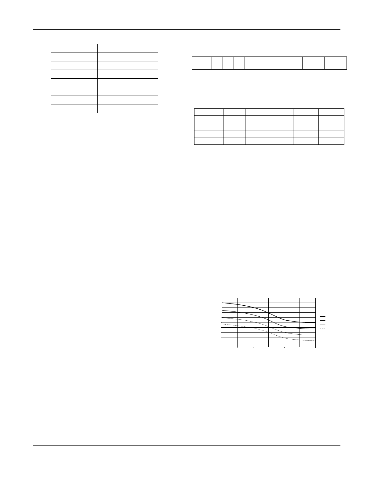
frequency setting, and can be shown in Figure 7.
When the tuning voltage is in the range from 0.9V to
1.4V, the VCO gain is at its maximum, approximately
32 to 35MHz/V. It is recommended that the varactor
voltage stays in this range.
The input capacitance at the varactor pin must be
taken into consideration when designing the PLL
loop filter. This is most critical when designing a loop
filter with high bandwidth, which gives relatively
small component values. The input capacitance is
approximately 6pF.
July 2006
Figure 7. RF Frequency vs. Varactor Voltage
and VCO Frequency bit (V
= 2.25V)
DD
17
M9999-092904
+1 408-944-0800
Page 18
Micrel MICRF506BML/YML
Pin 27
C
Pin 29
N
Charge Pump
A6..A0 D7 D6 D5 D4 D3 D2 D1 D0
0000010 CP_HI SC_by ‘0’ PA_by OUTS3 OUTS2 OUTS1 OUTS1
The charge pump current can be set to either 125µA
or 500µA by CP_HI (‘1’ → 500µA). This will affect
the loop filter component values, see “PLL Filter”
section. In most cases, the low current is best suited.
For applications using phase detector frequency and
high PLL bandwidth, the 500µA can be a better
choice.
PLL Filter
The design of the PLL filter will strongly affect the
performance of the frequency synthesizer. The PLL
filter is kept externally for flexibility. Input parameters
when designing the loop filter for the MICRF506 are
mainly the modulation method and the bit rate.
These choices will also affect the switching time and
phase noise.
The frequency modulation can be done in two
different ways with the MICRF506, either by VCO
modulation or by modulation with the internal
dividers (see chapter Frequency modulation for
further details). In the first case, the PLL needs to
lock on a new carrier frequency for every new data
bit. Now the PLL bandwidth needs to be adequately
high. It is recommended to use a third order filter to
suppress the phase detector frequency, as this is
not suppressed as much as when doing modulation
on the VCO with a lower bandwidth filter.
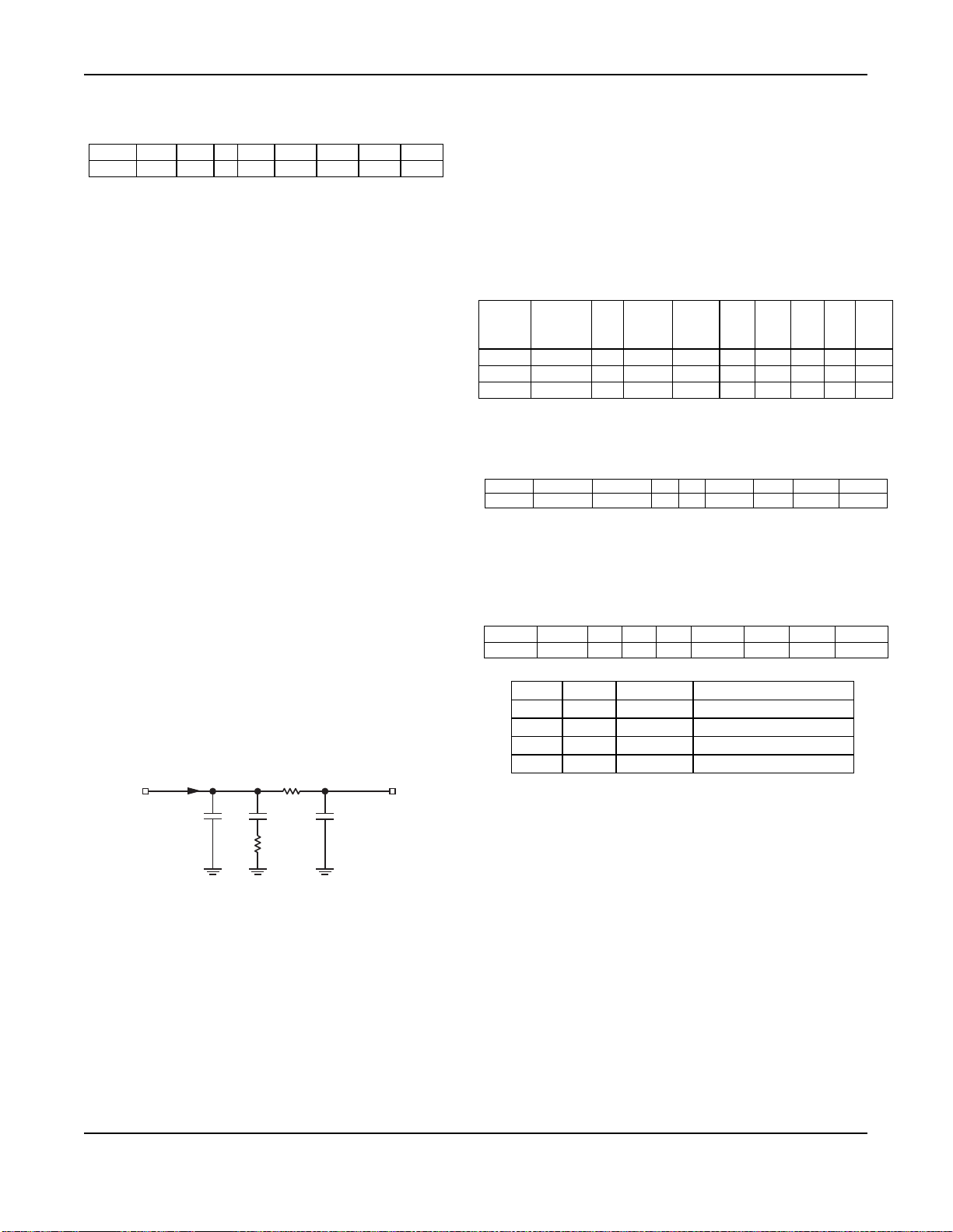
A schematic for a second (R2=0 and C3=NC) and
third order loop filter is shown in Figure 8.
P_OUT
R2
VARI
Table 9 shows three different loop filters, the two first
for VCO modulation and the last one for modulation
using the internal dividers. The component values
are calculated with RF frequency = 434MHz, VCO
gain = 32MHz/V and charge pump current = 125µA.
Other settings are shown in the table. The varactor
pin capacitance (pin 29) of 5pF does not influence
on the component values for the two filters with
lowest bandwidth.
PLL
Divider <20 13 86 500 150pF 10nF 18kΩ 82kΩ 4.7pF
Baud Rate
(kbaud/sec)
VCO >38.4 0.8 56 100 10nF 100nF 6.2kΩ 0 NC
VCO >125 3,2 56 100 680pF 6.8nF 22kΩ 0 NC
BW
(kHz)
Phase
Margin(˚)
Table 9. Loop Filter Components Values
Phase
Detector
Freq.
(kHz)
C1 C2 R1 R2 C3
Lock Detect
A6..A0 D7 D6 D5 D4 D3 D2 D1 D0
0000001 Modulat ion1 Modulation0 ‘0’ ‘0’ RSSI _en LD_en PF_FC1 PF_FC0
A lock detector can be enabled by setting LD_en
= 1. When pin LD is high, it indicates that the
PLL is in lock.
Modes of Operation
A6..A0 D7 D6 D5 D4 D3 D2 D1 D0
0000000 LNA_by PA2 PA1 PA0 Sync_en Mode1 Mode0 Load_en
Mode1 Mode0 State Comments
0 0 Power down Keeps register configuration
0 1 Standby Only crystal oscillator running
1 0 Receive Full receive
1 1 Transmit Full transmit ex PA state
C2
R1
C3C1
Figure 8. Second and Third Order Loop Filter
July 2006
18
M9999-092904
+1 408-944-0800
Page 19
Micrel MICRF506BML/YML
DATACLK
DATACLK
Transceiver Sync/Non-Synchronous Mode
A6..A0 D7 D6 D5 D4 D3 D2 D1 D0
0000000 LNA_by PA2 PA1 PA0 Sync_en Mode1 Mode0 Load_en
0000110 - Mod_clkS2 Mod_clkS1 Mod_clkS0 BitSync_clkS2 BitSync_clkS1 BitSync_clkS0 BitRate_clkS2
0000111 BitRate_clkS1 BitRate_clkS0 RefClk_K5 RefClk_K4 RefClk_K3 RefClk_K2 RefClk_K1 RefClk_K0
Sync_en State Comments
0
0 Tx: DataClk pin off
1
1 Tx: DATACLK pin on
Rx: Bit
synchronization off
Rx: Bit
synchronization on
When Sync_en = 1, it will enable the bit
synchronizer in receive mode. The bit synchronizer
clock needs to be programmed, see chapter Bit
synchronizer. The synchronized clock will be set out
on pit DATACLK.
In transmit mode, when Sync_en = 1, the clock
signal on pin DATACLK is a programmed bit rate
clock. Now the transceiver controls the actual data
rate. The data to be transmitted will be sampled on
rising edge of DATACLK. The micro controller can
therefore use the negative edge to change the data
to be transmitted. The clock used for this purpose,
BITRATE_CLK, is programmed in the same way as
the modulator clock and the bit synchronizer clock:
=
f
KBITRATE_CL
where:
f
BITRATE_CLK
: The clock frequency used to
control the bit rate, should be equal to the bit
rate (bit rate of 20 kbit/sec requires a clock
requency of 20kHz)
f
: Crystal oscillator frequency
XCO
Refclk_K: 6 bit divider, values between 1
and 63
BitRate_clkS: Bit rate setting, values
between 0 and 6
Data Interface
The MICRF506 interface can be divided in to two
separate interfaces, a “programming interface” and a
“Data interface”. The “programming interface” has a
three wire serial programmable interface and is
described in chapter Programming.
The “data interface” can be programmed to sync/non-synchronous mode. In synchronous mode the
Transparent reception of
data
Transparent transmission
of data
Bit-clock is generated by
transceiver
Bit-clock is generated by
transceiver
f
×
XCO
2Refclk_K
)-(7
kSBitRate_cl
MICRF506 is defined as “Master” and provides a
data clock that allows users to utilize low cost micro
controller reference frequency.
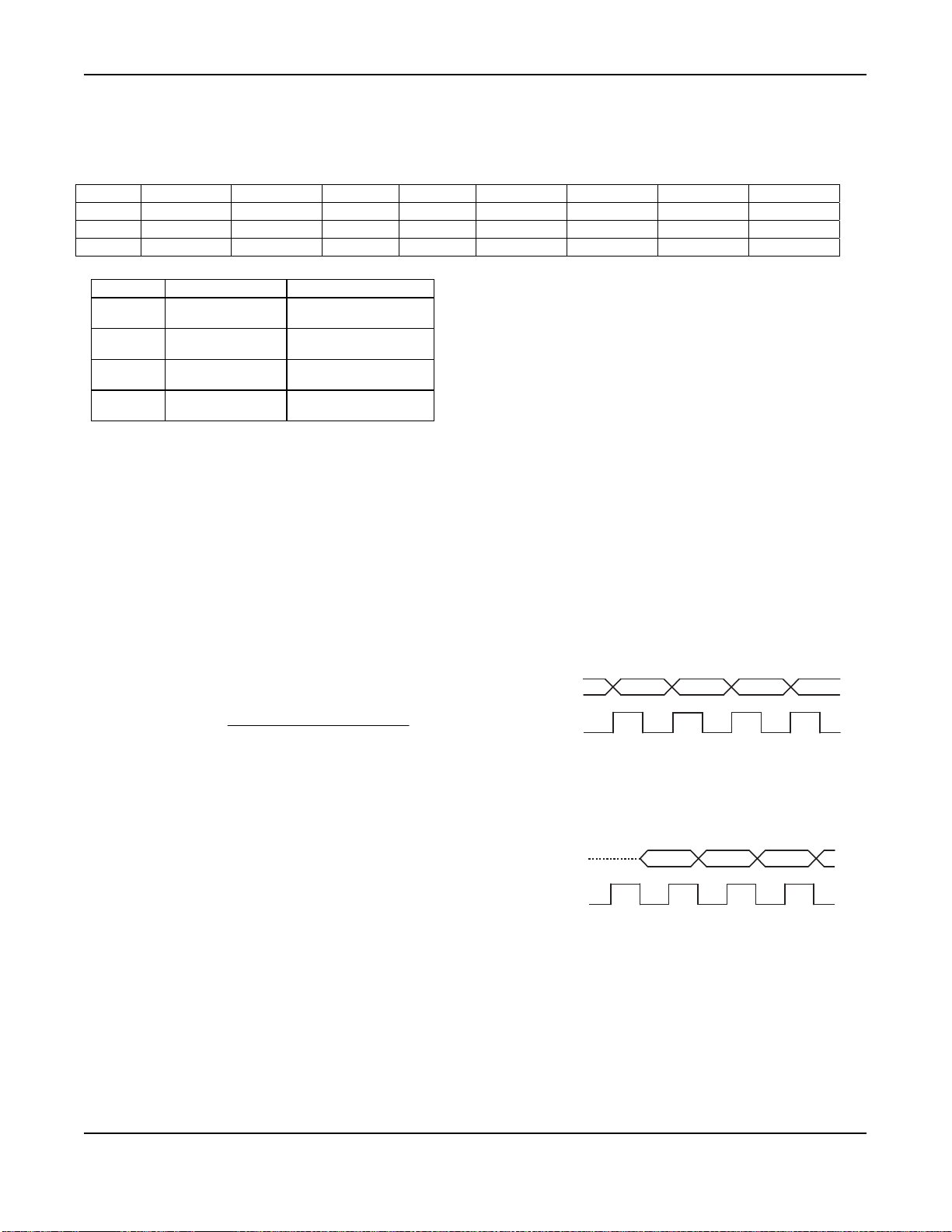
The data interface is defined in such a way that all
user actions should take place on falling edge and is
illustrated Figure 9 and 10. The two figures illustrate
the relationship between DATACLK and DATAIXO
in receive mode and transmit mode.
MICRF506 will present data on rising edge and the
“USER” sample data on falling edge in receive
mode.
DATAIXO
Figure 10. Data interface in Receive Mode
The User presents data on falling edge and
MICRF506 samples on rising edge in transmit mode.
DATAIXO
Figure 11. Data interface in Transmit Mode
When entering transmit mode it is important to keep
DATAIXO in tri-state from the time Tx-mode is
entered until user starts sending data. The data is
provided directly to the modulation circuit and
violation of this may/will cause abnormal behavior.
Depending upon the chosen FSK modulation, some
sort of encoding might be needed. The different
modulation types and encoding is described in
chapter Frequency modulation.
July 2006
19
M9999-092904
+1 408-944-0800
Page 20
Micrel MICRF506BML/YML
Receiver
The receiver is a zero intermediate frequency (IF)
type in order to make channel filtering possible with
low-power integrated low-pass filters. The receiver
consists of a low noise amplifier (LNA) that drives a
quadrature mixer pair. The mixer outputs feed two
identical signal channels in phase quadrature. Each
channel include a pre-amplifier, a third order SallenKey RC lowpass filter from strong adjacent channel
signals and finally a limiter. The main channel filter is
a switched-capacitor implementation of a six-pole
elliptic lowpass filte. The elliptic filter minimizes the
total capacitance required for a given selectivity and
dynamic range. The cut-off frequency of the SallenKey RC filter can be programmed to four different
frequencies: 100kHz, 150kHz, 230kHz and 340kHz.
The demodulator demodulates the I and Q channel
outputs and produces a digital data output. If detects
the relative phase of the I and Q channel signal. If
the I channel signal lags the Q channel, the FSK
tone frequency lies above the LO frequency (data
‘1’). If the I channel leads the Q channel, the FSK
tone lies below the LO frequency (data ‘0’). The
output of the receiver is available on the DataIXO
pin. A RSSI circuit (receive signal strength indicator)
indicates the received signal level.
Front End
A6..A0 D7 D6 D5 D4 D3 D2 D1 D0
0000000 LNA_by PA2 PA1 PA0 Sync_en Mode1 Mode0 Load_en
A low noise amplifier in RF receivers is used to
boost the incoming signal prior to the frequency
conversion process. This is important in order to
prevent mixer noise from dominating the overall
front-end noise performance. The LNA is a twostage amplifier and has a nominal gain of
approximately 23dB at 434MHz. The front end has a
gain of about 35dB to 38dB. The gain varies by 1-
1.5dB over a 2.0V to 2.5V variation in power supply.
The LNA can be bypassed by setting bit LNA_by to
‘1’. This can be useful for very strong input signal
levels. The front-end gain with the LNA bypassed is
about 12dB. The mixers have a going of about 10dB
at 434MHz. The differential outputs of the mixers
can be made available at pins IchOut and QchOut.
The output impedance of each mixer is about 8kΩ.
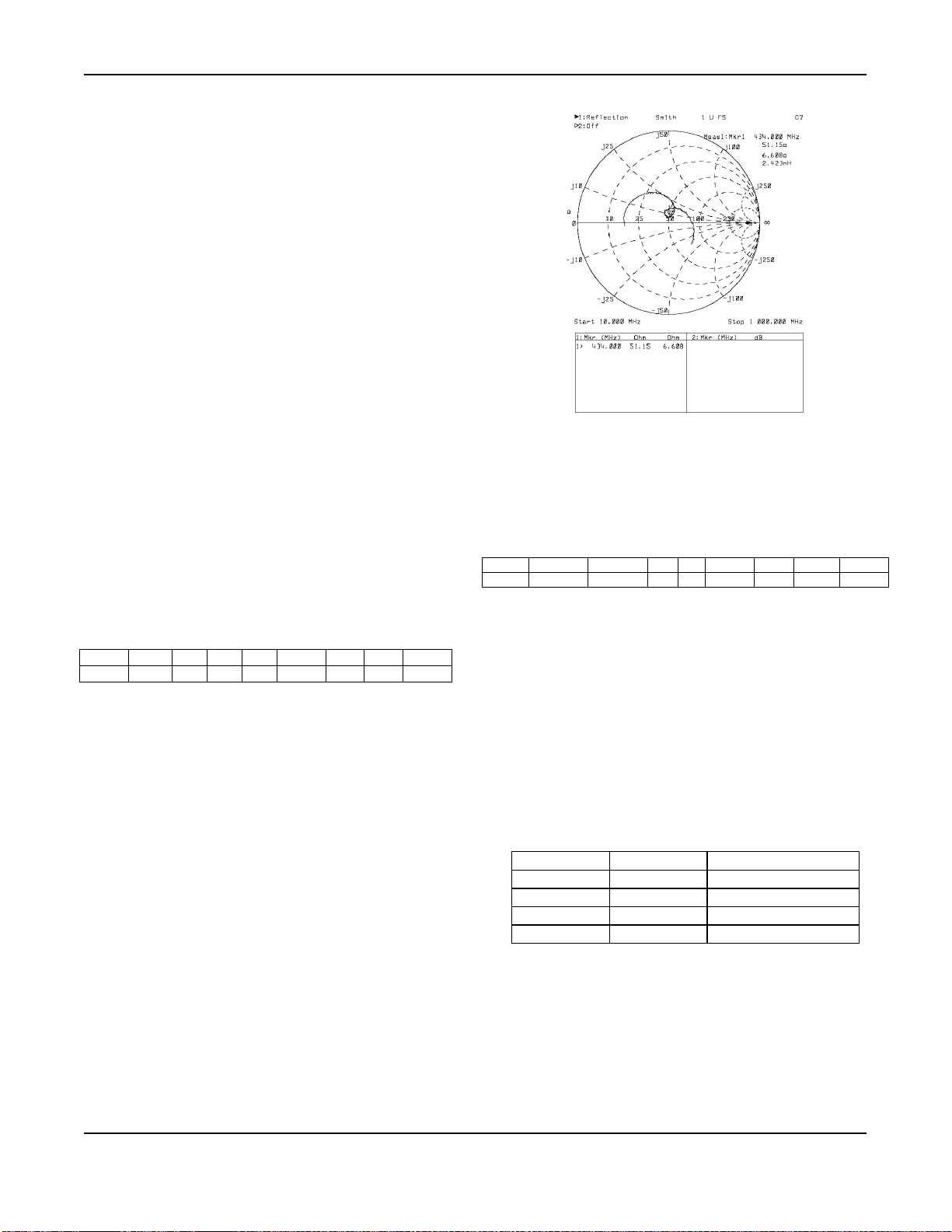
The input impedance is close to 50Ω as shown in
Figure 12, giving an input reflection of about -20dB.
The receiver does not require any matching network
to optimize the gain. However, a matching network is
recommended for harmonic suppression in Tx and
for improved selectivity in Rx.
July 2006
Figure 12. LNA Input Impedance
Sallen-Key Filters
A6..A0 D7 D6 D5 D4 D3 D2 D1 D0
0000001 Modulation1 Modulation0 ‘0’ ‘0’ RSSI_en LD_en PF_FC1 PF_FC0
Each channel includes a pre-amplifier and a prefilter,
which is a three-pole Sallen-Key lowpass filter. It
protects the following switched-capacitor filter from
strong adjacent channel signals, and it also works as
an anti-aliasing filter. The preamplifier has a gain of
22dB. The maximum output voltage swing is about
1.4Vpp for a 2.25V power supply. In addition, the IF
amplifier also performs offset cancellation. Gain
varies by less than 0.5dB over a 2.0 – 2.5V variation
in power supply. The third order Sallen-Key lowpass
filter is programmable to four different cut-off
frequencies according to the table below:
PF_FC1 PF_FC0 Cut-off Freq. (kHz)
0 0 100
0 1 150
1 0 230
1 1 340
20
M9999-092904
+1 408-944-0800
Page 21
Micrel MICRF506BML/YML
Pin 14
SI
Switched Capacitor Filter
A6..A0 D7 D6 D5 D4 D3 D2 D1 D0
0001000 ‘1’ ScClk_X2 ‘0’ ScClk4 ScClk3 ScClk2 ScClk1 ScClk0
The main channel filter is a switched-capacitor
A6..A0 D7 D6 D5 D4 D3 D2 D1 D0
0000001 Modulation1 Modulation0 ‘0’ ‘0’ RSSI_en LD_en PF_FC1 PF_F C0
Baudrate: The baud rate given is bit/sec
RSSI
implementation of a six-pole elliptic low pass filter.
The elliptic filter minimized the total capacitance
required for a given selectivity and dynamic range.
The cut-off frequency of the switched-capacitor filter
is adjustable by changing the clock frequency.
The clock frequency is designed to be 20 times the
cut-off frequency. The clock frequency is derived
from the reference crystal oscillator. A
programmable 6-bit divider divides the frequency of
the crystal oscillator. To generate the correct nonoverlapping clock-phases needed by the filter this
frequency is then divided by 4. The cut-off frequency
of the filter is given by:
f
f
CUT
=
XCO
40 ⋅ ScClk
: Filter cutoff frequency
f
CUT
f
: Crystal oscillator frequency
XCO
ScClk: Switched capacitor filter clock, bits
ScClk5-0
For instance, for a crystal frequency of 16MHz and if
the 6 bit divider divides the input frequency by 4 the
cut-off frequency of the SC filter is 16MHz/(40 x 4) =
100kHz. 1
st
order RC low pass filters are connected
to the output of the SC filter-to-filter the clock
frequency.
The lowest cutoff frequency in the pre- and the main
channel filter must be set so that the received signal
is passed with no attenuation, which is frequency
deviation plus modulation. If there are any frequency
offset between the transmitter and the receiver, this
must also be taken into consideration. A formula for
the receiver bandwidth can be summarized as
follows:
fBW = + f
OFFSET
+ f
DEV
+ Baudrate / 2
where
f
: Needed receiver bandwidth, fcut above
BW
should not be smaller than f
f
: Total frequency offset between
OFFSET
BW
[Hz]
receiver and transmitter [Hz]
f
: Single-sided frequency deviation, see
DEV
2.2
2
1.8
1.6
1.4
RSSI [V]
1.2
1
0.8
0.6
-125 -115 -105 -95 -85 -75 -65 -55 -45 -35 -25
Figure 13. RSSI Voltage
RSSI
Figure 14. RSSI Network
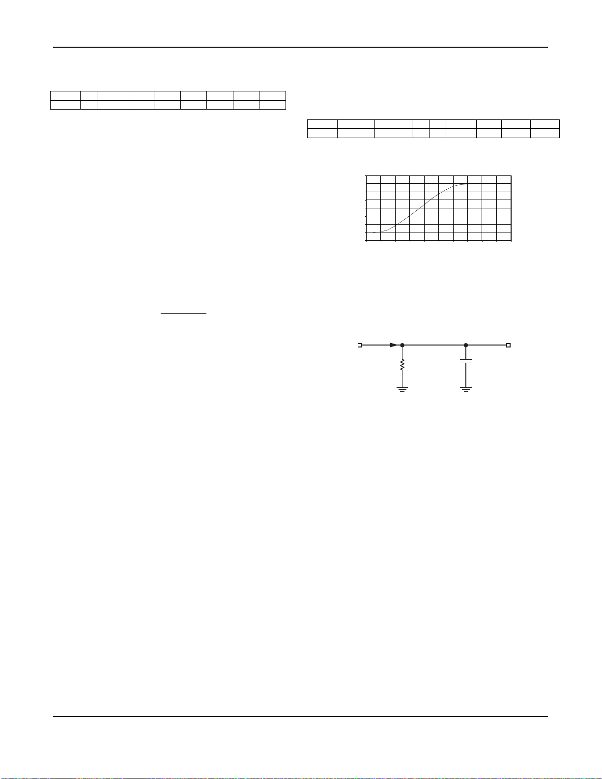
A Typical plot of the RSSI voltage as function of
input power is shown in Figure 13. The RSSI has a
dynamic range of about 50dB from about -110dBm
to -60dBm input power.
The RSSI can be used as a signal presence
indicator. When a RF signal is received, the RSSI
output increases. This could be used to wake up
circuitry that is normally in a sleep mode
configuration to conserve battery life.
Another application for which the RSSI could be
used is to determine if transmit power can be
reduced in a system. If the RSSI detects a strong
signal, if could tell the transmitter to reduce the
transmit power to reduce current consumption.
RSSI
33kohm, 1nF, 125kbps, BW=200kHz, Vdd=2.5V
Pin [dBm]
R2
33k
C10
1nF
RS
chapter Modulator on how to calculate [Hz]
July 2006
21
M9999-092904
+1 408-944-0800
Page 22
Micrel MICRF506
FEE
A6..A0 D7 D6 D5 D4 D3 D2 D1 D0
0010101 - - - - FEEC_3 FEEC_2 FEEC_1 FEEC _0
0010110 FEE_7 FEE_6 FEE_5 FEE_4 FEE_3 FEE_2 FEE_1 FEE_0
The Frequency Error Estimator (FEE) uses
information from the demodulator to calculate the
frequency offset between it’s receive frequency and
the transmitter frequency. The output of the FEE can
be used to tune the XCO frequency, both for
production calibration and for compensation for
crystal temperature drift and aging.
The inputs to the FEE circuit are the up and down
pulses from the demodulator. Every time a ‘1’ is
updated, an UP-pulse is coming out of the
where FEE is the value stored in the FEE register,
(Fp is the single sided frequency deviation, P is the
number of symbols/data bit counted and R is the
symbol/data rate. A positive Foffset means that the
received signal has a higher frequency than the
receiver frequency. To compensate for this, the
receivers XCO frequency should be increased (see
ANNEX A) on how to tune the XCO frequency based
on the FEE value).
It is recommended to use Mode UP+DN for two
reasons, you do not need to know the actual
frequency deviation and this mode gives the best
accuracy.
demodulator, and the same with the DN-pulse every
time the ‘0’ is updated. The expected number of
pulses for every received symbol is 2 times the
modulation index (∆).
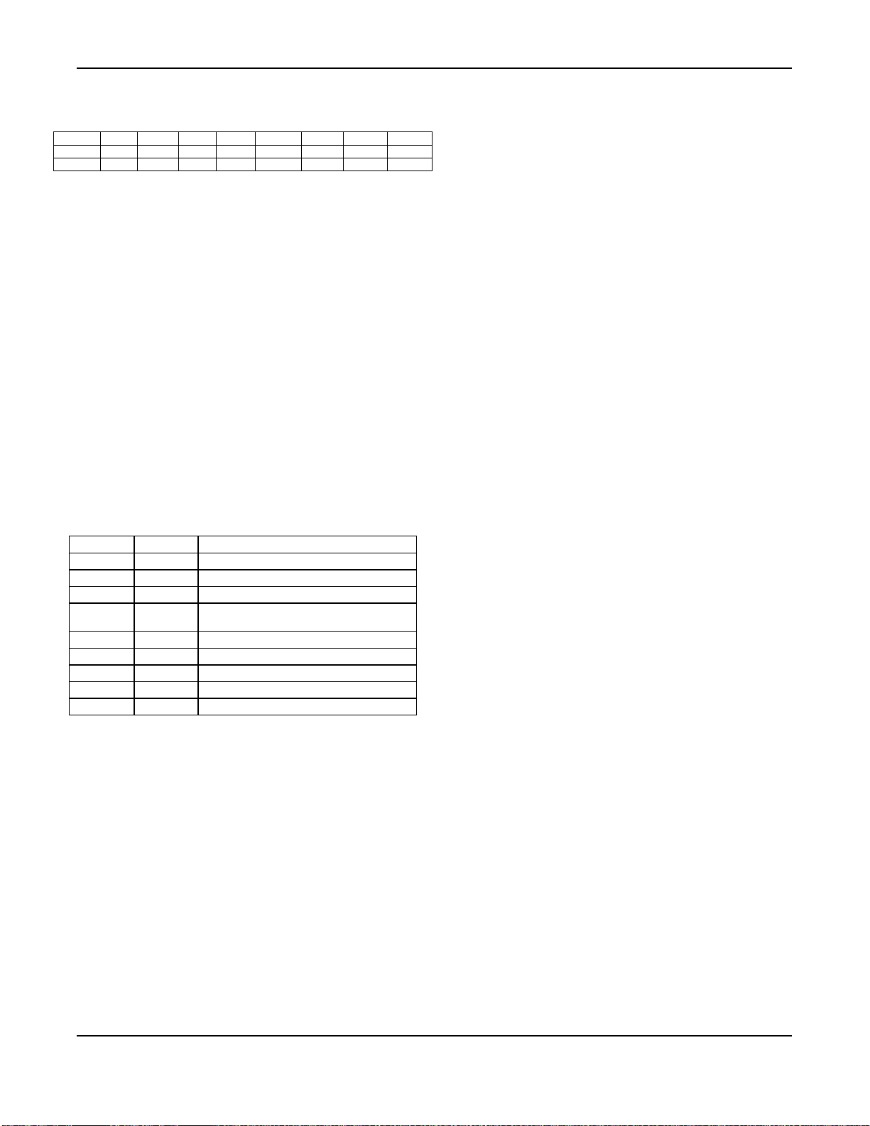
The FEE can operate in three different modes;
counting only UP-pulses, only DN-pulses or counting
UP+DN pulses. The number of received symbols to
be counted is either 8, 16, 32 or 64. This is set by
the FEEC_0…FEEC_3 control bit, as follows:
FEEC_1 FEEC_0 FEE Mode
0 0 Off
0 1 Counting UP pulses
1 0 Counting DN pulses
1 1 Counting UP and DN pulses. UP increments
FEEC_3 FEEC_2 No. of symbols used for the measurement
0 0 8
0 1 16
1 0 32
1 1 65
the counter, DN decrements it.
Table 10. FEEC Control Bit
The result of the measurement is the FEE value, this
can be read from register with address 0010110b.
Negative values are stored as a binary no between
0000000 and 1111111. To calculate the negative
value, a two’s complement of this value must be
performed. Only FEE modes where DN-pulses are
counted (10 and 11) will give a negative value.
When the FEE value has been read, the frequency
offset can be calculated as follows:
Mode UP: Foffset = R/(2P)x(FEE-∆Fp)
Mode DN: Foffset = R/(2P)x(FEE+∆Fp)
Mode UP+DN: Foffset = R/(4P)x(FEE)
July 2006
22
M9999-092904
+1 408-944-0800
Page 23

Micrel MICRF506BML/YML
Bit Synchronizer
A6..A0 D7 D6 D5 D4 D3 D2 D1 D0
0000110 - ModclkS2 ModclkS1 ModclkS0 BitSync_clkS2 BitSync_clkS1 BitSync_clkS0 BitRate_clkS2
0000111 BitRate_clkS1 BitRate_clkS0 RefClk_K5 RefClk_K4 RefClk_K3 RefClk_K2 RefClk_K1 RefClk_K0
A bit synchronizer can be enabled in receive mode
by selecting the synchronous mode (Sync_en=1).
The DataClk pin will output a clock with twice the
frequency of the bit rate (a bit rate of 20 kbit/sec
gives a DataClk of 20 kHz). A received symbol/bit on
DataIXO will be output on rising edge of DataClk.
The micro controller should therefore sample the
symbol/bit on falling edge of DataClk.
The bit synchronizer uses a clock which needs to be
programmed according to the bit rate. The clock
frequency should be 16 times the actual bit rate (a
bit rate of 20 kbit/sec needs a bit synchronizer clock
with frequency of 320 kHz). The clock frequency is
set by the following formula:
XCO
BITSYNC_CLK
f
=
Refclk_K × 2
f
(7-BITSYNC_c lk S )
where
f
BITSYNC_CLK
: The bit synchronizer clock
frequency (16 times higher than the bit rate)
f
: Crystal oscillator frequency
XCO
Refclk_K: 6 bit divider, values between 1 and
63
BitSync_clkS: Bit synchronizer setting, values
between 0 and 7
Refclk_K is also used to derive the modulator clock
and the bit rate clock.
At the beginning of a received data package, the bit
synchronizer clock frequency is not synchronized to
the bit rate. When these two are maximum offset to
each other, it takes 22 bit/symbols before
synchronization is achieved.
July 2006
23
M9999-092904
+1 408-944-0800
Page 24
Micrel MICRF506
Transmitter
Power Amplifier
A6..A0 D7 D6 D5 D4 D3 D2 D1 D0
0000000 LNA_by PA2 PA1 PA0 Sync_en Mode1 Mode0 Load_en
0000001 Modulation1 Modulation0 ‘0’ ‘0’ RSSI_en LD_en PF_FC1 PF_FC0
0000010 CP_HI SC_by ‘0’ PA_By OUTS3 OUTS2 OUTS1 OUTS0
The maximum output power is approximately 10dBm
for a 50Ω load. For maximum output power the load
seen by the PA must be resistive. Higher output
power can be obtained by decreasing the load
impedance. However, this will be in conflict with
obtaining impedance match in the LNA. The output
power is programmable in seven steps, with
approximately 3dB between each step. This is
controlled by bits PA2 – PA0.
The power amplifier can be turned off by setting PA2
– PA0 = 0.
For all other combinations the PA is on and has
maximum power when PA2 – PA0 = 1.
The PA will be bypassed if PA_by=1. Output power
will drop ~22dB. It is still possible to control the
power by PA2 – PA0.
The output power varies about 3dB over power
supply 2.0V to 2.5V and about 2dB over temperature
-40˚C to +85˚C. The 2
nd
and 3rd harmonic of the PA
are as follows:
nd
2
harmonic: <-16dBm
rd
3
harmonic: <-8dBm
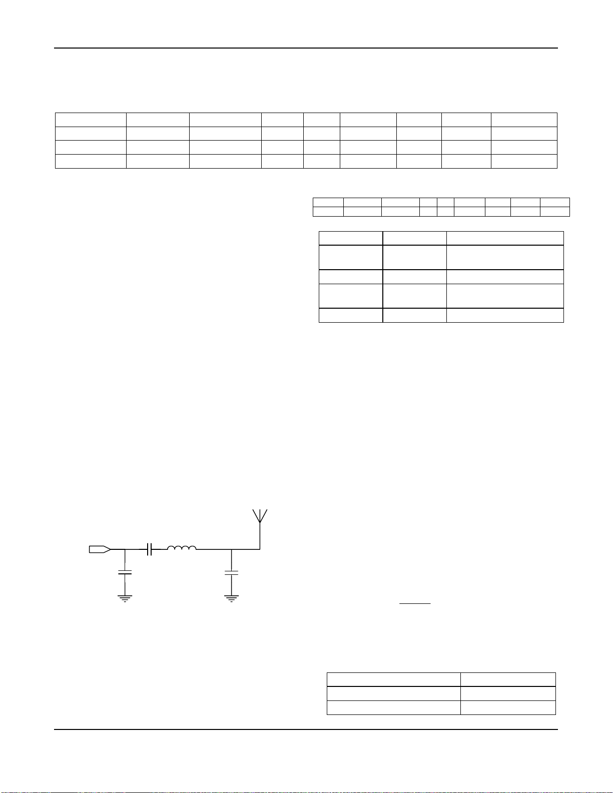
To reduce the emission of harmonics, an LC filter
can be added between the ANT pin and the antenna
as shown in Figure 15.
C5
L1
ANT
C4
18pF
47pF
12nH
15pF
C6
Figure 15. LC Filter
This filter is designed for the 434MHz band with
50Ohm terminations. The component values may
have to be tuned to compensate for the layout
parasitics. This filter may also increase the receiver
selectivity.
Frequency Modulation
A6..A0 D7 D6 D5 D4 D3 D2 D1 D0
0000001 Modulation1 Modulation0 ‘0’ ‘0’ RSSI_en LD_en PF_FC1 PF_F C0
Modulation1 Modulation0 Modulation Type
0 0 Closed loop modulation
using modulator
0 1 Not in use
1 0 FSK applied using two
sets of dividers
1 1 Not in use
Table 11. Modulation Bit Setting
When Modulation1 and Modulation0 is 00, the
modulator needs to be programmed properly, see
“Modulator” section. The modulation signal will now
be applied directly on the phase locked VCO. It is
therefore important that the PLL bandwidth is not too
high, as this will remove the modulation. See “PLL
Filter” section on how to calculate the PLL
components. When using the modulator the
modulation signal is applied to the VCO and
therefore some sort of encoding is needed.
The level of encoding is determined by the PLL loop
filter bandwidth and data rate. Two of the most
common encoding techniques are Manchester
encoding and 3B4B. Other encoding schemes may
also be used.
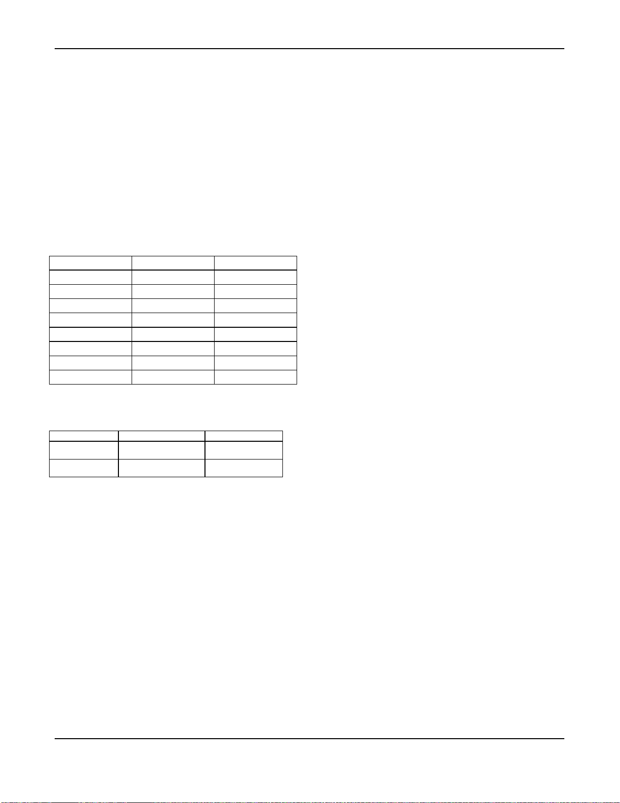
Manchester encoding is when one bit is encoded in
to a two-bit word and is shown in Table 10. When
using Manchester encoding the maximum overhead
is 100%. When selecting PLL loop filter it is
important to note that the min baud rate is equal to:
f
f
baud_min
baud_min
=
baud /s
4
: The minimum frequency of the baud
rate [Hz]
baud/s: Elements per second (encoded data)
Data Word
“0” “10”
“1” “01”
July 2006
24
M9999-092904
+1 408-944-0800
Page 25
Micrel MICRF506BML/YML
Table 12. Manchester Encoding
Another much more efficient encoding type is 3B4B
where three data bits are encoded into a four-bit
word. The reason for encoding is to minimize the DC
component in the modulated data. To have minimum
DC component each four bit word should include
two elements of “1” and two elements of “0”.
Following this guidance only 6 out of 8 word
complies and two encoded words needs special
precaution. Whenever 000 and 111 data appear, the
user must set/clear a flag that indicate if last
encoded word was “Word A” and select the
respective encoded word shown in Table 11.
Data Word A Word B
000 1011 0100
001 1100
010 0011
011 1010
100 0101
101 1001
110 0110
111 1101 0010
Table 13. 3B4B Encoding
Data bits Encoded words Comments
000 000 000 000 000 1011 0100 1011 0100 1011 A Flag indicates if “Word
111 111 010 110 000 1101 0010 0011 0110 1011 A Flag indicates if “Word
Table 14. Example of 3B4B encoding
A” has been used
A” has been used
When Modulation1 Modulation0 is 10, two sets of
divider values need to be programmed. The formula
for calculating the M, N and A values is given in
chapter Frequency synthesizer. The divider values
stored in the M0-, N0-, and A0- registers will be used
when transmitting a ‘0’ and the M1-, N1-, and A1registers will be used to transmit a ‘1’. The difference
between the two carrier frequencies corresponds to
the double sided frequency modulation. Opposite
from the modulation with the modulator, the PLL
shall now lock on a new frequency for every change
in the transmitted data. The PLL bandwidth therefore
needs to be relatively high, higher bit rate requires a
higher PLL bandwidth and vice versa. The data to
be transmitted shall be applied to pin DataIXO (see
chapter Transceiver sync-/non-synchronous mode
on how to use the pin DataClk). The DataIXO pin is
set as input in transmit mode and output in receive
mode. When set as input, a weak voltage divider will
set the level to Vdd/2, when it is not pulled up or
down by the controller. When using the modulator, it
is important that the DataIXO is kept tristated until
the transmission shall begin (when PLL is in lock
and the PA is turned on). When Data IXO is
tristated, the PLL will lock on the LO frequency
(used in receive mode). When DataIXO is set either
high or low, the RF frequency will be shifted up or
down, centered around the LO-frequency. This is
only important when using the modulator, for the
other modulation method, if DATAIXO is tristated,
the M0-, N0- and A0-registers will be used.
July 2006
25
M9999-092904
+1 408-944-0800
Page 26
Micrel MICRF506BML/YML
M
M
M
Modulator
A6..A0 D7 D6 D5 D4 D3 D2 D1 D0
0000100 Mod_F2 Mod_F1 Mod_F0 Mod_I4 Mod_I3 Mod_I2 Mod_I1 Mod_I0
0000101 - - ‘0’ ‘1’ Mod_A3 Mod_A2 Mod_A1 Mod_A0
0000110 - Mod_clkS2 Mod_clkS1 Mod_clkS0 BitSync_clkS2 BitSync_clkS1 BitSync_clkS0 BitRate_clkS2
0000111 BitRate_clkS1 BitRate_clkS0 RefClk_K5 RefClk_K4 RefClk_K3 RefClk_K2 RefClk_K1 RefClk_K0
The modulator will create a waveform with
programmable amplitude and frequency. This
Mod_clka
Mod_clkb
waveform is fed into a modulation varactor in the
VCO, which will create the desired frequency
modulation. The frequency spectrum can be
narrowed by increasing the rise-and fall times of the
waveform.
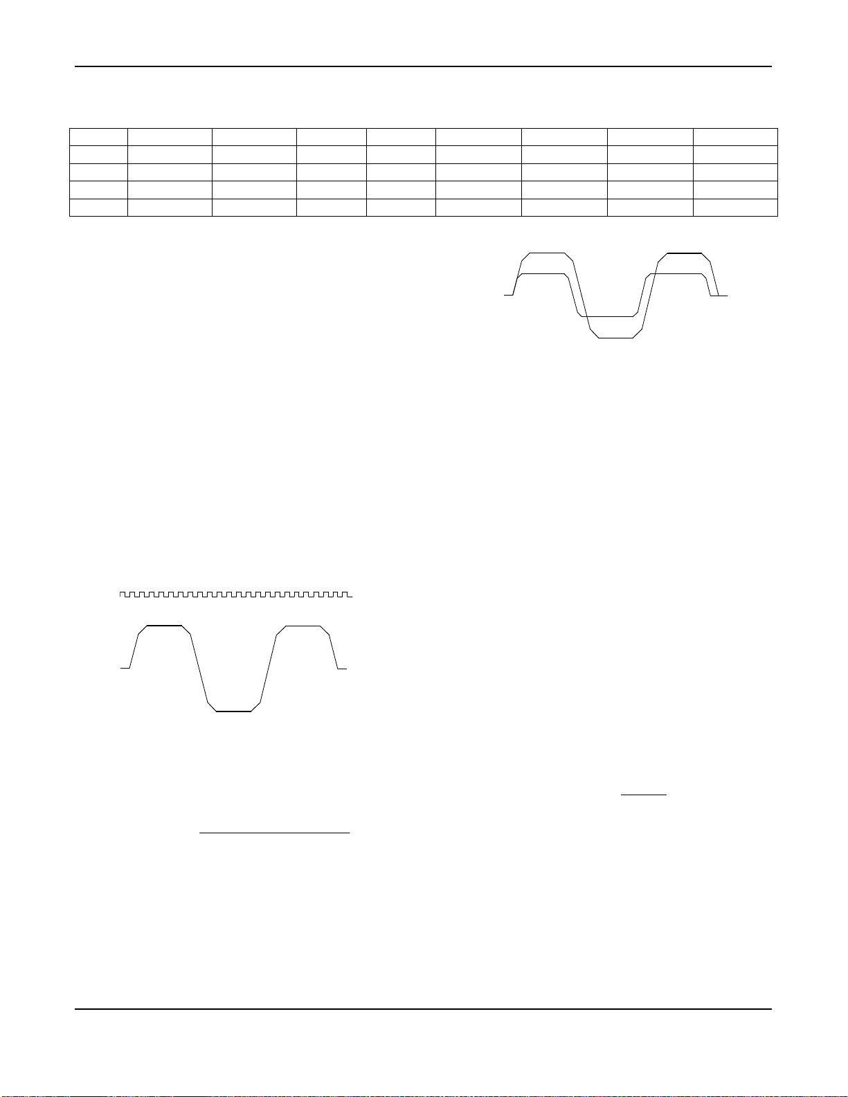
The modulator waveform is created by charging and
discharging a capacitor. A modulator clock controls
the timing, as shown in Figure19. For every rise-and
fall edge, 4 clock periods are being used. The
charging current during these 4 clock periods are not
equal, this is to reduce the high frequency
components in the waveform, which in turn will
narrow the frequency spectrum.
The frequency deviation can be set in three different
ways, as will be explained below. A formula for
setting the desired deviation is given at the end of
this chapter.
odulator Clock
A f
corresponds to a signal filtered in a Gaussian filter
with a Bandwidth Period product (BT) of 1. When BT
is increased, the waveform will be less filtered.
Minimum BT is 1 (f
Figure 20 shows two waveforms with BT=1 and
BT=2, i.e. the f
the bit rate. When changing the BT factor, the
charge-and discharge times will also be changed,
and therefore the frequency deviation, as shown in
Figure 19.
od_clkb > Mod_clka
Figure 20. Two Different Modulator Clock Setting
MOD_CLK
of 8 times the bit rate (as in Figure 20)
MOD_CLK
MOD_CLK
is 8 times the bitrate).
is 8 and 16 times higher than
odulator Waveform
Modulator Current
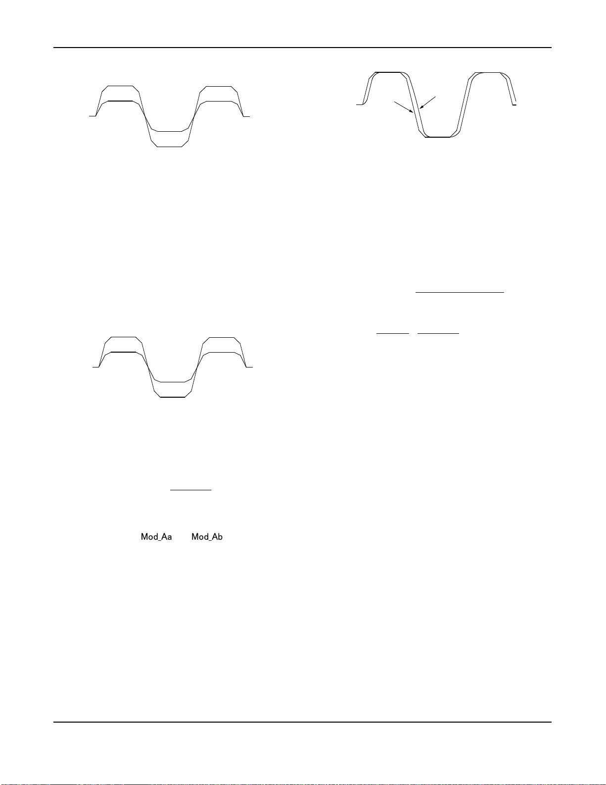
The current used during the rise- and fall times can
be programmed with the Mod_I4..Mod_I0 bit, the
last one being LSB. Figure 21 shows two waveforms
generated with two different currents, where
. Higher current will give a
Figure 19. Modulator Waveform and Clock
Modulator Clock
higher frequency deviation and vice versa. The
effect of modulator clock and MOD_1 is illustrated
by:
The modulator clock frequency is set by:
f
MPOD_CLK
f
=
XCO
×
Mod_clkS−
2Refclk_K
)(7
where f
MOD_CLK
Figure 19, f
is the modulator clock shown in
is the crystal oscillator frequency
XCO
Refclk_K is a 6 bit number and Mod_clkS is a 3 bit
To avoid saturation in the modulator it is important
not to exceed maximum Mod_I. Maximum Mod_I for
a given fMOD_clk is given by:
MOD_I
number. Mod_clkS can be set to a value between 0
and 7. The modulator clock frequency should be set
according to the bit rate and shaping.
July 2006
where INT() returns the integer part of the argument.
26
IbModIaMod __ >
f
DEVIATION
= INT(f
MAX
MOD_1
×
f
MOD_CLK
MOD_CLK
⋅ 28 × 106)-1
M9999-092904
+1 408-944-0800
Page 27
Micrel MICRF506BML/YML
M
M
Mod_la
Mod_lb
od_la > Mod_lb
Mod_filter off
Mod_filter on
Figure 21. Two Different Modulator Current Settings
Modulator Attenuator
A third way to set the deviation is by programming
the modulator attenuator, Mod_A2..Mod_A0, the last
being LSB. The purpose of the attenuator is to allow
small deviations when the bit rate is small and/or the
BT is small (these settings will give a relatively slow
modulator clock, and therefore long rise- and fall
times, which in turn results in large frequency
deviations). In addition, the attenuator will improve
the resolution in the modulator.
Mod_Aa
Mod_Ab
Figure 23. Modulator Waveform with and withou t
Mod_F=0 disables the modulator filter and Mod_F=7
gives most filtering. Figure 22 shows a waveform
with and without the filter.
Calculation of the Frequency Deviation
The parameters influencing the frequency deviation
can be summarized in the following equations:
f
DEV
f
=
MOD_CLK
Mod_I
f
MOD_CLK
=
Filtering
Refclk_K × 2
1
×
1+ Mod_A
f
XCO
(7−Mod_clkS )
× C1+ C2× f
()
RF
od_Ab > Mod_Ab
Figure 22. Two Different Modulator Attenuator
Settings
The effect of the attenuator is given by:
f
DEVIATION
1
×
1+ Mod_A
Figure 22 shows two waveforms with different
Mod_A
attenuator setting:
Mod_A
b
a
<
. If Mod_A
is increased, the frequency deviation is lowered and
vice versa.
Modulator Filter
To reduce the high-frequency components in the
generated waveform, a filter with programmable cut-
Where:
: Single sided frequency deviation
f
DEV
[Hz]
f
: Crystal oscillator frequency [Hz]
XCO
f
: Center frequency [Hz]
RF
Refclk_K: 6 bit divider, values between 1
and 63
Mod_clkS: Modulator clock setting, values
between 0 and 7
f
MOD_CLK
: Modulator clock frequency,
derived from the crystal
frequency, Refclk_K and
Mod_clkS
Mod_I: Modulator current setting,
values between 0 and 31
Mod_A: Modulator attenuator setting,
values between 0 and 15
C1: -2.17·10
10
C2: 82
off frequency can be enabled. This is done using
Mod_F2..Mod_F0, the least one being LSB. The
Mod_F should be set according to the formula:
July 2006
27
M9999-092904
+1 408-944-0800
Page 28

Micrel MICRF506BML/YML
The modulator filter will not influence on the
frequency deviation as long as the programmed cutoff frequency is above the actual bit rate.
The frequency deviation must be programmed so
that the modulation index (2 x single sided frequency
deviation/Baudrate [bps]) always is greater than or
equal to 2 including the total frequency offset
between the receiver and the transmitter:
f
= Baudrate + f
DEV
OFFSET
The calculated f
should be used to calculate the
DEV
needed receiver bandwidth, see chapter Switched
capacitor filter.
If FEE > 0: LO is too low, increase LO by decreasing
XCO_tune value
v.v. for FEE < 0
FEE field holds a number in the range -128, … ,
127. However, it keeps counting above/below the
range, which is:
If FEE = -128 and still counting dwn-pulses:
1) =>-129 = +127
2) 126
3) 125
…
Using the XCO-tune Bits
The RF chip has a built-in mechanism for tuning the
frequency of the crystal oscillator and is often used
in combination with the Frequency Error Estimator
(FEE). The XCO tuning is designed to eliminate or
reduce initial frequency tolerance of the crystal
and/or the frequency stability over temperature. If
the value in XCO_tune is increased (adding
capacitance), the frequency will decrease.
The XCO uses two external capacitors (see figure
5). The value of these will strongly affect the tuning
range. With a 16.0 MHz crystal (TN4-26011 from
Toyocom), and external capacitor values of 1.5 pF,
the tuning range will be approximately symmetrical
around the center frequency. A XCO_tune >16 will
decrease the frequency and vice versa (see figure
6).
A procedure for using the XCO_tune feature in
combination with the FEE is given below. The
MICRF506 measures the frequency offset between
the demodulated signal and the LO and tune the
XCO so the LO frequency is equal to received
carrier frequency.
A procedure like this can be called during production
(storing the calibrated XCO_tune value), at regular
intervals or implemented in the communication
protocol when the frequency has changed.
The FEE can count “UP”-pulses and/or “DOWN”pulses (pulses out of the demodulator when a logic
“1” or logic “0”, resp.., is received). The FEE can
count pulses for n bits, where n = 8, 16, 32 or 64.
Example: In FEE, count up+down pulses, counting 8
bits:
A perfect case ==> FEE = 0
July 2006
28
M9999-092904
+1 408-944-0800
Page 29

Micrel MICRF506BML/YML
To avoid this situation, always make sure max count
is between limits. Suggestion: Count for 8 (or 16)
bits only.
Procedure description:
In the procedure below, UP+DWN pulses are
counted, and only the sign of the FEE is used. The
value of n is 8 or 16.
Assumption:
A transmitter is sending a 1010… pattern at the
correct frequency and bitrate.
The wanted receiver frequency is the mid-point
between the “0” and “1” frequencies.
Input:
Nothing
Output
The best XCO_tune value (giving the lowest IFEEI)
Local variables:
XCO_Present: (5-bit) holds present value in
XCO_tune bits
XCO_Step: (4-bit) holds increment/decrement of
XCO_tune bits
SCO_Sign: (1 bit) holds POS or NEG
(increment/cerement) increasing LO is done by
reducing the XCO_tune value
XCO TUNE PROCEDURE
INT:
XCO_Present = 0
XCO_Step = 32
XCO_Sign = NEG
Control_Word =
Default RX, clocks match transmitter
LOOP:
XCO_Step = XCO_Step/2
XCO_Sign == POS?
Yes --> XCO_Present- = XCO_Step // increase LO
No --> XCO_Present+ = XCO_Step // decrease LO
XCO_tune bits = CXO_Present
Program RFChip
Delay > n bits
Read FEE
FEE > 0?
Yes --> XCO_Sign = POS
No --> XCO_Sing = NEG // negative or == 0
XCO_Step > 1?
Yes --> Branch to LOOP
No -->
XCO_Sing ==POS?
Yes --> XCO_Present- = 1
Branch to FIN
FIN: RETURN, return-value = XCO_Present
July 2006
29
M9999-092904
+1 408-944-0800
Page 30
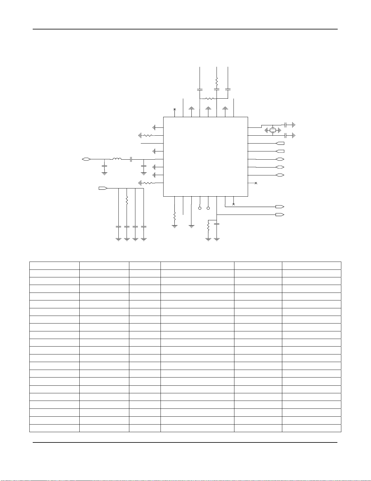
Micrel MICRF506BML/YML
Typical Application
V2P5_2
V2P5_2
V2P5_2
C3
nc
R1
6k2
C2
C1
100nF
R2
0R
10nF
V2P5_2
32
31
30
29
28
NC
1
2
3
4
5
6
7
8
RFGND
PTATBIAS
RFVDD
RFGND
ANT
RFGND
GND
NC
R3 27k
V2P5_3
L1
C5
V2P5_1
47pF
R7
10R
C11
10nF
V2P5_2
C12
1nF
50ohm line50ohm line
C4
18pF
R4
nc
V2P5_3
C13
1nF
ANT
RFVDD
C6
15pF
12nH
V2P5_0
C10
1nF
VCOVDD
CIBIAS
IFVDD
9
10
11
V2P5_0
R5
82k
GND
VARIN
VCOGND
MICRF506
MLF32
IFGND
ICHOUT
QCHOUT
12
13
TP1
TP2
R6
33k
V2P5_1
27
26
25
24
DIGVDD
CP_OUT
DIGGND
XTALOUT
23
XTALIN
CS
SCLK
IO
DATAlXO
DATACLK
NC
RSSI
LD
14
NC
15
16
C7
1nF
TSX 10A, 16MHz
22
21
20
19
18
17
C9
1.5pF
3
Y1
2
4
C8
1
1.5pF
CS
SCLK
IO
DATAIXO
DATACLK
LD
RSSI
MICRF506 – MLF32
Item Part Value Description Manufacturer Part Numner
1 C1 10nF 10nF X7R ±10% 0603 50V Kyocera CM105X7R103K50A
2 C2 100nF 100nF X7R ±10% 0603 16V Kyocera CM105X7R104K16A
3 C3 NC
4 C4 18pF 18pF COG ±5% 0603 50V Kyocera CM105CG180J50A
5 C5 47pF 47pF COG ±5% 0603 50V Kyocera CM105CG470J50A
6 C6 15pF 15pF COG ±5% 0603 50V Kyocera CM105CG150J50A
7 C7 1nF Optional Kyocera CM105X7R102K50A
8 C8 1.5pF 1.5pF COG ±0.25pF 0603 50V Kyocera CM105CG1R5C50A
9 C9 1.5pF 1.5pF COG ±0.25pF 0603 50V Kyocera CM105CG1R5C50A
10 C10 1nF 1nF X7R ±10% 0603 50V Kyocera CM105X7R102K50A
11 C11 10nF 10nF X7R ±10% 0603 50V Kyocera CM105X7R103K50A
12 C12 1nF 1nF X7R ±10% 0603 50V Kyocera CM105X7R102K50A
13 C13 1nF 1nF X7R ±10% 0603 50V Kyocera CM105X7R102K50A
14 R1 6.2k 6.2k ±1% 0603 50V Kyocera CR10-6201F
15 R2
0
Ω
0
Ω
16 R3 27k 27k ±1% 0603 50V Kyocera CR10-2702F
17 R5 82k 82k ±1% 0603 50V Kyocera CR10-8202F
18 R6 33k Optional Kyocera CR10-3302F
19 R7
10
Ω
10R ±1% 0603 50V Kyocera CR10-10R0F
20 L1 12nH 12nH ±5% 0603 Coilcraft 0603CS-12NXJB
21 Y1 16MHz 16MHz, 9pF, 10/10ppm Toyocom TN4-26011
±1% 0603 50V
Kyocera CJ10-000
July 2006
30
M9999-092904
+1 408-944-0800
Page 31
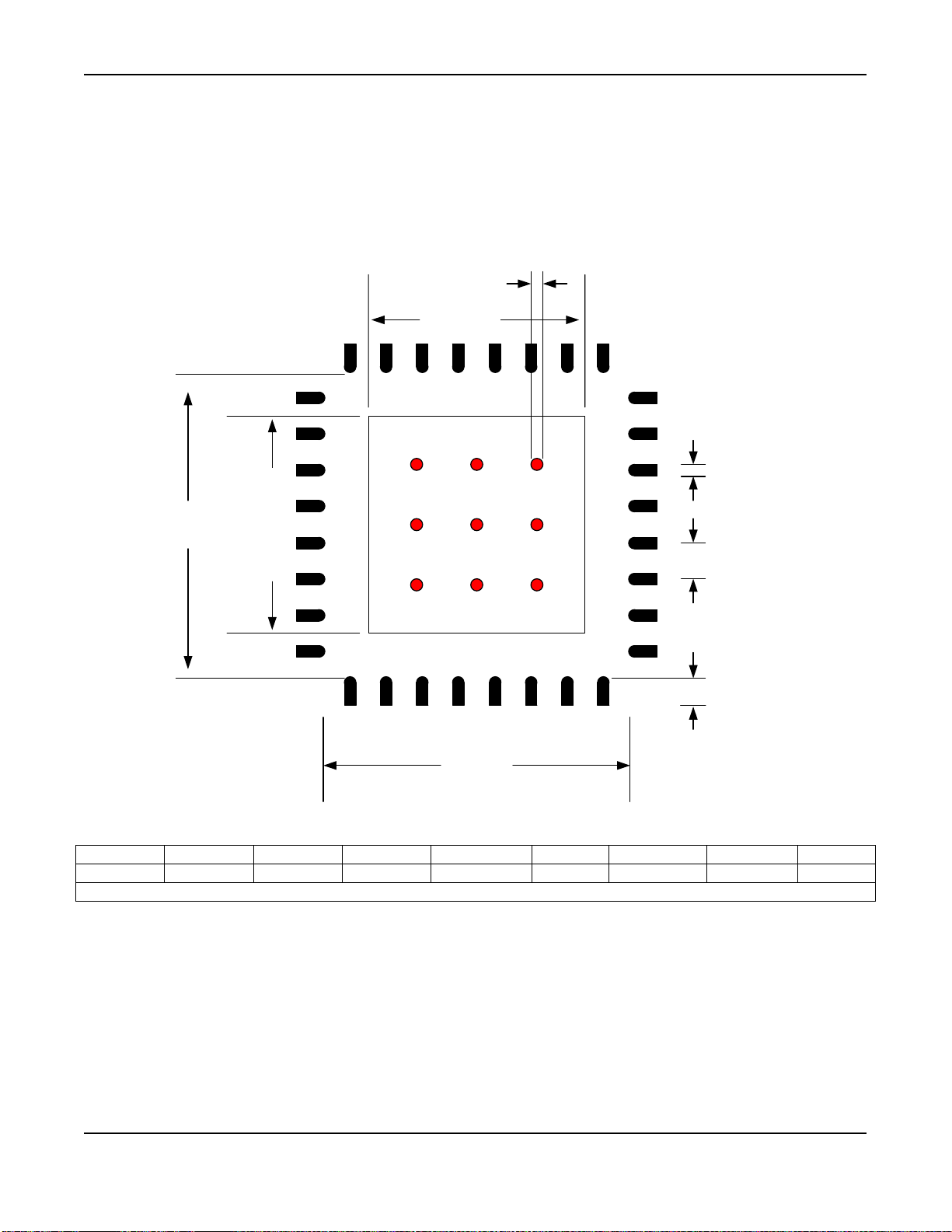
Micrel MICRF506BML/YML
MICRF506BML/YML Land pattern
Figure below shows recommended land pattern. Red circles indicate Thermal/RFGND via’s. Recommended size
is 0.300-0.350mm with a pitch of 1mm. The recommended minimum number of via’s are 9 and they should be
directly connected to ground plane providing the best RF ground and thermal performance. For best yield plugged
or open via’s should be used.
d
D2'
X
SE
E2'
e
Y
SD
D2’ E2’ SD SE d e X Y Units
3.4 ±0.02 3.4 ±0.02 4.2 ±0.05 4.2 ±0.05 0.325 ±0.25 0.5 0.23 ±0.02 0.5 ±0.02 mm
Red circle indicates Thermal Via. Size 0.300-0.350mm
July 2006
31
M9999-092904
+1 408-944-0800
Page 32
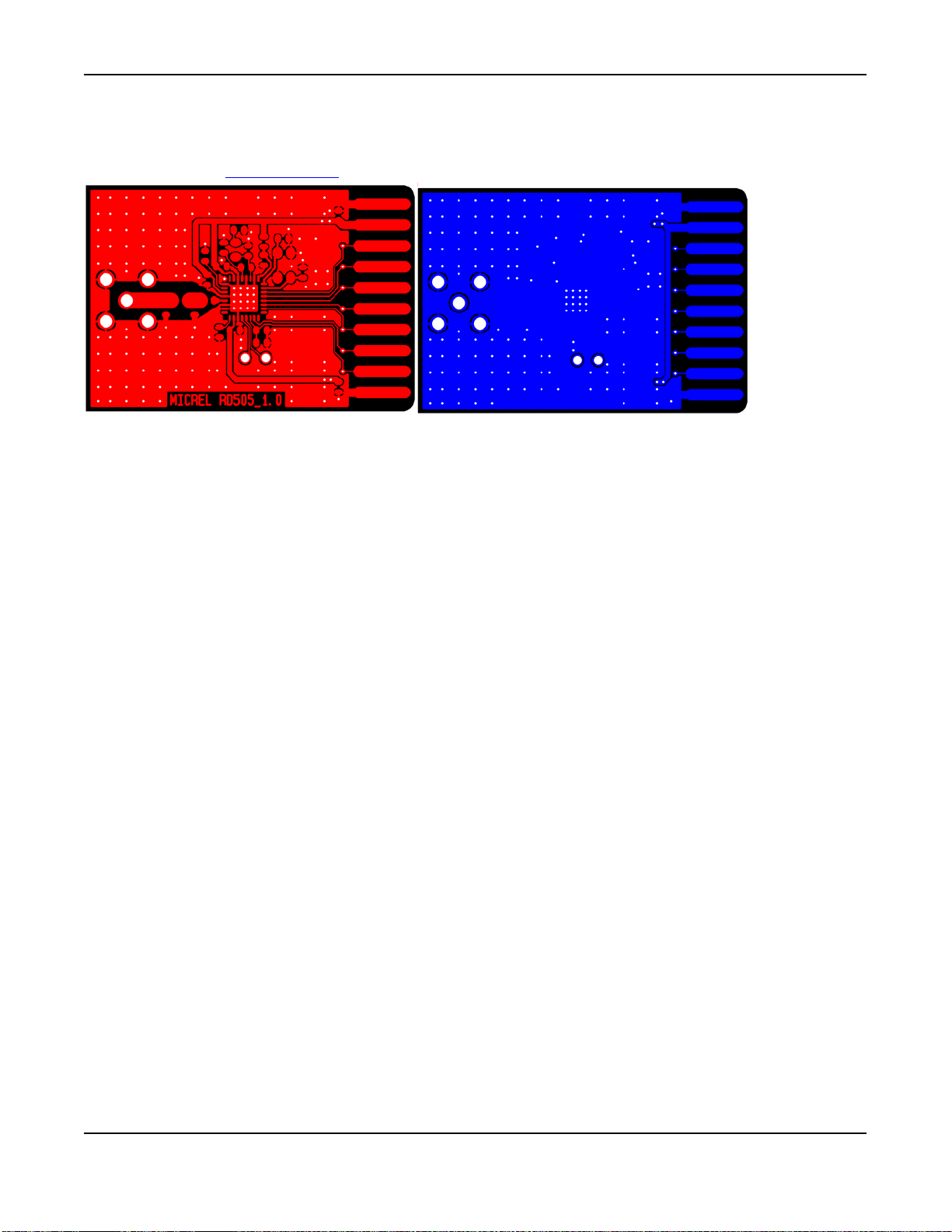
Micrel MICRF506BML/YML
Layout Considerations
The MICRF506 is a highly integrated RF IC with only a few “hot” pins, however it is suggested to study available
reference design on www.micrel.com before starting with schematics and layout.
•
To ensure the best RF design it is important to plan the layout and dedicate area for the different circuitry.
Good RF engineering is to start with the RF circuitry making sure that general RF guidelines are met
(following points). Separate noisy circuitry and RF by placing it on the opposite side maximizing the
distance between the circuitry. The RF circuitry should be placed as close to what is considered the
ground spot (EG battery) to avoid ground currents. Place the RF circuitry in a position that ensure as
short and straight trace to the antenna connection to avoid reflections.
•
Proper ground is needed. If the PCB is 2-layer, the bottom layer should be kept only for ground. Avoid
signal traces that split the ground plane. For a 4-layer PCB, it is recommended to keep the second layer
only for ground.
•
A ground via should be placed close to all the ground pins. The bottom ground (heat sink) pad should be
penetrated with >9 ground via’s. These via’s should be “open” or “plugged” to avoid air pockets caused by
the solder past. If such air pockets appear, the air will expand during the reflow process and may/will
cause the device to twist/move.
•
The antenna pin (pin 5) has an impedance of ~50 ohm. The antenna trace should be kept to 50 ohm to
avoid signal reflection and loss of performance. Minor deviations can be compensated by matching the
LC filter. Any transmission line calculator can be used to find the needed trace width given a board build
up. Ex: A trace width of 75 mil (1.9 mm) gives 50 impedance on a FR4 board (dielectric cons=4.4) with
copper thickness of 35
•
RF circuitry is sensitive to voltage supply and therefore caution should be taken when choosing power
circuitry. To achieve the best performance, low noise LDO’s with high PSSR should be chosen. What is
present on the voltage supply will be directly modulated to the RF spectrum causing degradation and
regulatory issues. To make sure you have the right selection, please contact local sales for the latest
Micrel offerings in power management and guidance. To avoid “pickup” from other circuitry on the VDD
lines, it is recommended to route the VDD in a star configuration with decoupling at each circuitry and at
the common connection point (see above layout). If there are noisy circuitry in the design, it is strongly
recommended to use a separate power supply and/or place low value resistors (10ohms), inductors in
series with the power supply line into these circuitry.
•
It is recommended to connect the PLL loop filter to VDD (C1, C3 and R1). The VDD connection should be
placed as close to pin 31 (VCOVDD) as possible. The MICRF506 has a integrated VCO where the
resonator circuit (varactor ) has a reference to VDD. With a common reference point, the MICRF506
(PLL) will somewhat compensate for noise present on the VDD.
•
PLL loop filter components C1, C2, C3, R1 and R2 should have a compact layout and should be placed
as close to pin 27 and 29. Avoid signal traces/bus and noisy circuitry around/close/under this area.
•
Digital high speed logic or noisy circuitry should/must be at a safe distance from RF circuitry or RF VDD
as this might/will cause degradation of sensitivity and create spurious emissions. Example of such
circuitry is LCD display, charge pumps, RS232, clock / data bus etc.
July 2006
µ
m and height (layer 1-layer 2 spacing) of 1.00 mm.
32
M9999-092904
+1 408-944-0800
Page 33
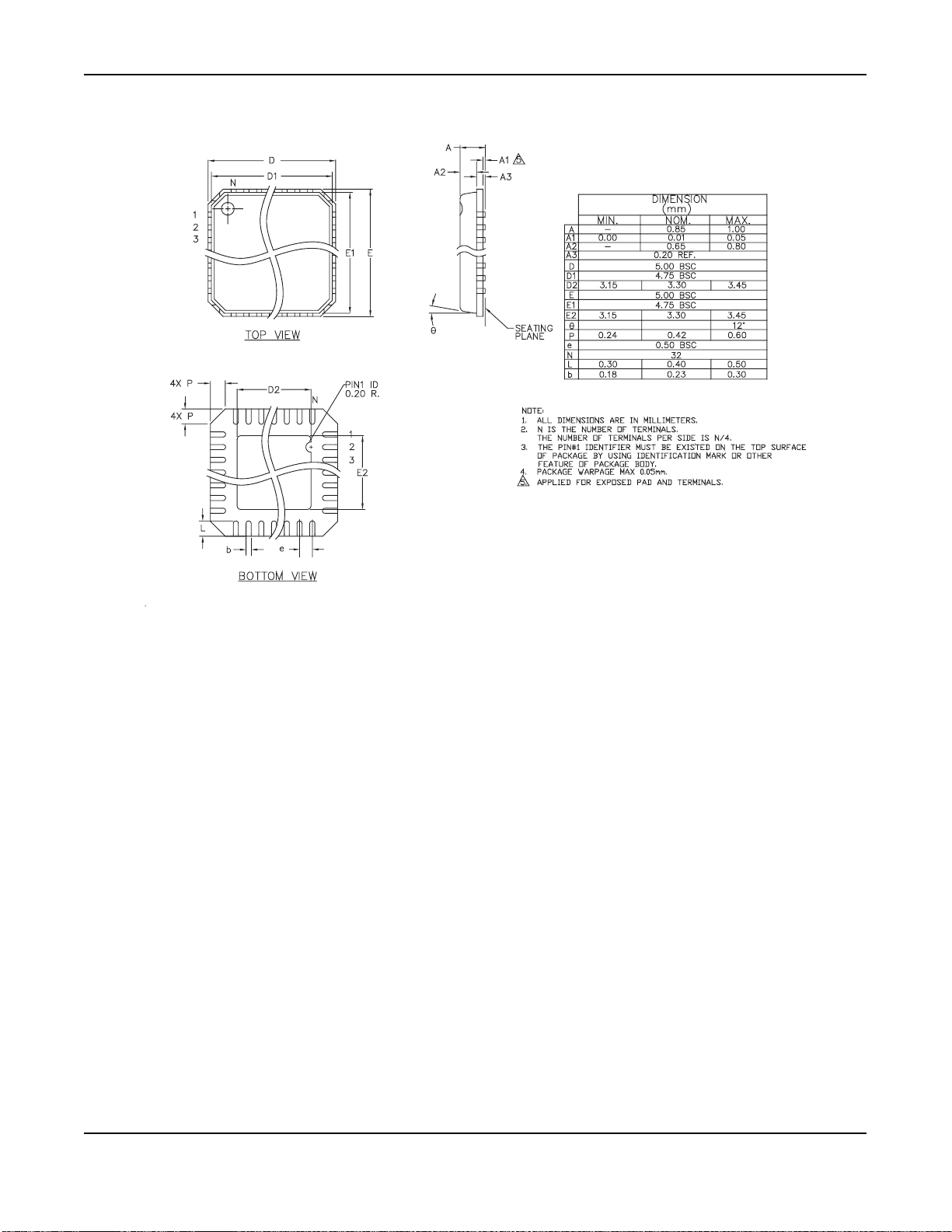
Micrel MICRF506BML/YML
Package Information MICRF506BML
MICRF505BML
32-Pin MLF (B)
July 2006
33
M9999-092904
+1 408-944-0800
Page 34
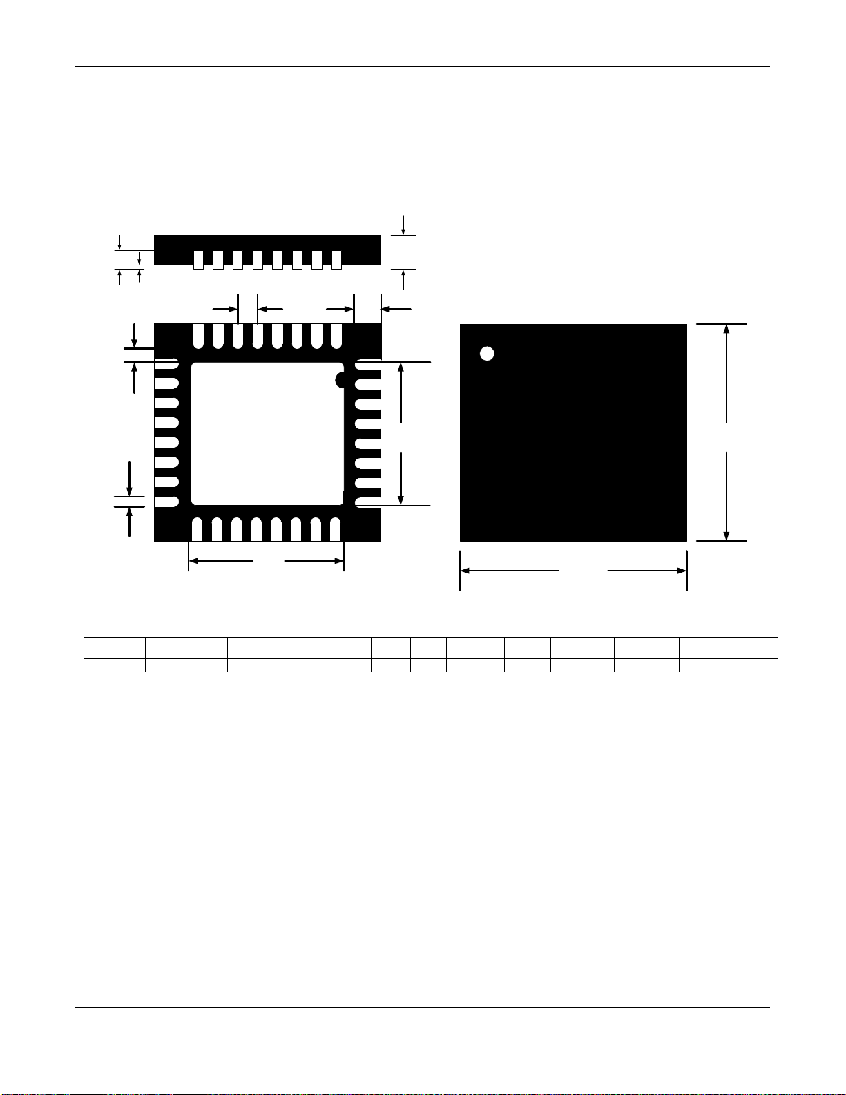
Micrel MICRF506BML/YML
Package Information MICRF506YML
Side view
H
2
h
e
C
PL
b
D2
Bottom view
H
L
E2
D
Top view
D D2 E E2 e b L C
5.0 3.10±0.10 5.0 3.10±0.10 0.5 0.25 0.4±0.05 0.20 0.85±0.05 0.00~0.05 0.2 mm
H h H2Units
PL
E
July 2006
34
M9999-092904
+1 408-944-0800
Page 35
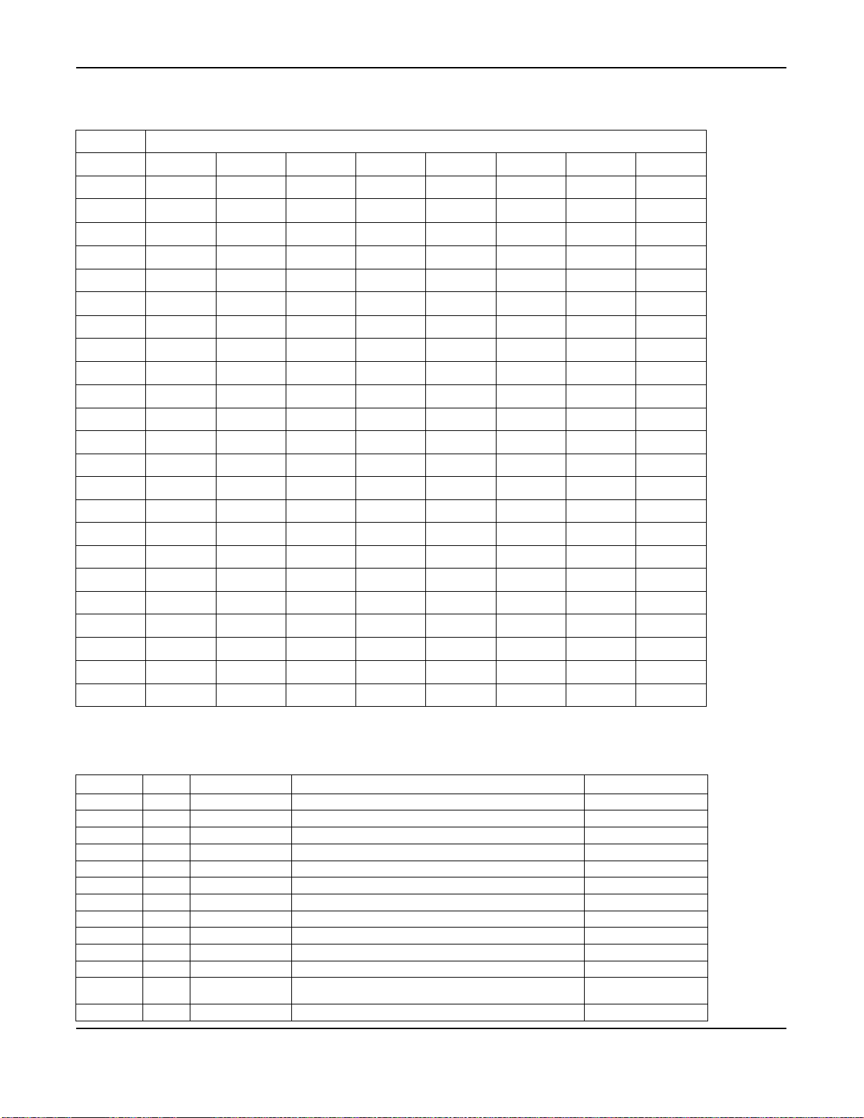
Micrel MICRF506BML/YML
Overview of programming bit
Address Data
A6..A0 D7 D6 D5 D4 D3 D2 D1 D0
0000000
0000001
0000010
0000011
0000100
0000101
0000110
0000111
0001000
0001001
0001010
0001011
0001100
0001101
0001110
0001111
0010000
0010001
0010010
0010011
0010100
0010101
0010110
LNA_by PA2 PA1 PA0 Sync_en Mode1 Mode0 Load_en
Modulation1 Modulation0
CP_HI SC_by
IFBias_s
(“1”)
Mod_F2 Mod_F1 Mod_F0 Mod_I4 Mod_I3 Mod_I2 Mod_I1 Mod_I0
- -
- Mod_clkS2 Mod_clkS1 Mod_clkS0 BitSync_clkS2 BitSync_clkS1 BitSync_clkS0 BitRate_clkS2
BitRate_clkS1 BitRate_clkS0 RefClk_K5 RefClk_K4 RefClk_K3 RefClk_K2 RefClk_K1 RefClk_K0
SC_HI
(“1”)
PrescalMode_s
(“0”)
- - A0_5 A0_4 A0_3 A0_2 A0_1 A0_0
- - - - N0_11 N0_10 N0_9 N0_8
N0_7 N0_6 N0_5 N0_4 N0_3 N0_2 N0_1 N0_0
- - - - M0_11 M0_10 M0_9 M0_8
M0_7 M0_6 M0_5 M0_4 M0_3 M0_2 M0_1 M0_0
- - A1_5 A1_4 A1_3 A1_2 A1_1 A1_0
- - - - N1_11 N1_10 N1_9 N1_8
N1_7 N1_6 N1_5 N1_4 N1_3 N1_2 N1_1 N1_0
- - - - M1_11 M1_10 M1_9 M1_8
M1_7 M1_6 M1_5 M1_4 M1_3 M1_2 M1_1 M1_0
Div2_HI
(“1”)
- - - - FEEC_3 FEEC_2 FEEC_1 FEEC_0
FEE_7 FEE_6 FEE_5 FEE_4 FEE_3 FEE_2 FEE_1 FEE_0
IFA_HG
(“1”)
ScClk_X2
(“1”)
Prescal_s
(“0”)
LO_IB1
(“0”)
OL_opamp_en
(“0”)
VCO_by
(“0”)
VCO_BIAS_s
(“0”)
Mod_FHG
(“0”)
ScSW_en
(“0”)
XCOAR_en
(”1”)
LO_IB0
(“1”)
PA_LDc_en
(”0”)
PA_by OUTS3 OUTS2 OUTS1 OUTS0
VCO_IB2 VCO_IB1 VCO_IB0 VCO_freq1 VCO_freq0
Mod_shape
(“1”)
ScClk4 ScClk3 ScClk2 ScClk1 ScClk0
XCOtune4 XCOtune3 XCOtune2 XCOtune1 XCOtune0
PA_IB4
(”0”)
RSSI_en LD_en PF_FC1 PF_FC0
Mod_A3 Mod_A2 Mod_A1 Mod_A0
PA_IB3
(”0”)
PA_IB2
(”0”)
PA_IB1
(”1”)
PA_IB0
(“1”)
Table 1: Detailed description of programming bit
ADR # BIT # NAME DESCRIPTION COMMENTS
0000000 7 By_LNA LNA bypass on/off
6 PA2 Power amplifier level, 3.bit Ref. Table 6
5 PA1 Power amplifier level, 2.bit Ref. Table 6
4 PA0 Power amplifier level, 1.bit Ref. Table 6
3 Sync_en Synchronizer Mode bit Ref. Table 3
2 Mode1 Main Mode selection 2. Bit Ref. Table 2
1 Mode0 Main Mode selection 1. Bit Ref. Table 2
0 Load_en Load generation (1=enable)
0000001 7 Modulation1 Modulation selection 2.bit Ref. Table 4
6 Modulation0 Modulation selection 1.bit Ref. Table 4
5 OL_opamp_en “0” mandatory. Opamp in OpenLoop circuit (0=disable)
4 PA_LDc_en
3 RSSI_en RSSI function (1=enable)
July 2006
“0” mandatory. PA controlled by Lock Detect
(0=disable) Ref. Table 6
35
M9999-092904
+1 408-944-0800
Page 36
Micrel MICRF506BML/YML
2 LD_en Lock detect function (1=enable)
1 PF_FC1 Prefilter corner frequency 2.bit Ref. Table 5
0 PF_FC0 Prefilter corner frequency 1.bit Ref. Table 5
0000010 7 CP_HI High charge-pump current (0=125uA, 1=500uA)
6 SC_by Bypass of Switched Capacitor filter (1=enable)
5 VCO_by “0” mandatory. Bypass of VCO (1=enable)
4 PA_by Bypass of PA (1=enable)
3 OUTS3 Test pins output 4.bit Ref. Table 8
2 OUTS2 Test pins output 3.bit Ref. Table 8
1 OUTS1 Test pins output 2.bit Ref. Table 8
0 OUTS0 Test pins output 1.bit Ref. Table 8
0000011 7 IFBias_s “1” mandatory.
6 IFA_HG “1” mandatory. High gain setting in preamplifier
5 VCO_Bias_s
4 VCO_IB2 VCO bias current setting, 3. bit (111 = highest current)
3 VCO_IB1 VCO bias current setting, 2. bit
2 VCO_IB0 VCO bias current setting, 1. bit
1 VCO_freq1 Frequency setting of VCO, 2. bit (11=highest frequency)
0 VCO_freq0 Frequency setting of VCO, 1.bit
0000100 7 Mod_F2 Modulator filter setting, MSB (0=filter active)
6 Mod_F1 Modulator filter setting
5 Mod_F0 Modulator filter setting, LSB
4 Mod_I4 Modulator current setting, MSB
3 Mod_I3 Modulator current setting
2 Mod_I2 Modulator current setting
1 Mod_I1 Modulator current setting
0 Mod_I0 Modulator current setting, LSB
0000101 7 --------- Reserved/not in use
6 --------- Reserved/not in use
5 Mod_FHG “0” mandatory. Modulator Test bit.
4 Mod_shape “1” mandatory. Modulator shape enable
3 Mod_A3 Modulator attenuator setting, MSB (1=attenuator active)
2 Mod_A2 Modulator attenuator setting
1 Mod_A1 Modulator attenuator setting
0 Mod_A0 Modulator attenuator setting, LSB
0000110 7 --------- Reserved/not in use
6 Mod_clkS2 Modulator clock setting 3.bit, MSB
5 Mod_clkS1 Modulator clock setting 2.bit
4 Mod_clkS0 Modulator clock setting 1.bit, LSB
3 BitSync_clkS2 BitSync clock setting 3.bit, MSB
2 BitSync_clkS1 BitSync clock setting 2.bit
1 BitSync_clkS0 BitSync clock setting 1.bit, LSB
0 BitRate_clkS2 Bitrate clock setting 3.bit, MSB
0000111 7 BitRate_clkS1 Bitrate clock setting 2.bit
6 BitRate_clkS0 Bitrate clock setting 1.bit. LSB:
5 RefClk_K5 Reference clock divider 6.bit, MSB
4 RefClk_K4 Reference clock divider 5.bit
3 RefClk_K3 Reference clock divider 4.bit
2 RefClk_K2 Reference clock divider 3.bit
1 RefClk_K1 Reference clock divider 2.bit
0 RefClk_K0 Reference clock divider 1.bit, LSB
0001000 7 SC_HI “1” mandatory. High current in Switched Cap filter
6 ScClk_X2 “1” mandatory. Switched Cap clock multiplied by two
5 ScSw_EN “0” mandatory. Switch cap switch enable
“0” mandatory. Select separate bias for VCO on
VCOBias pin (1=enable)
July 2006
36
M9999-092904
+1 408-944-0800
Page 37
Micrel MICRF506BML/YML
4 ScClk4 SwitchCap clock divider 5.bit, MSB
3 ScClk3 SwitchCap clock divider 4.bit
2 ScClk2 SwitchCap clock divider 3.bit
1 ScClk1 SwitchCap clock divider 2.bit
0 ScClk0 SwitchCap clock divider 1.bit, LSB
0001001 7 PrescalMode_s
6 Prescal_s “0” mandatory. Selects pulse swallow prescaler.
5 XCOAR_en “1” mandatory. Set XCO amplitude regulation on.
4 XCOtune4 Crystal oscillator trimming, LSB
3 XCOtune3 Crystal oscillator trimming
2 XCOtune2 Crystal oscillator trimming
1 XCOtune1 Crystal oscillator trimming
0 XCOtune0 Crystal oscillator trimming, MSB
0001010 7 --------- Reserved/not in use
6 --------- Reserved/not in use
5 A0_5 A0-counter 6.bit
4 A0_4 A0-counter 5.bit
3 A0_3 A0-counter 4.bit
2 A0_2 A0-counter 3.bit
1 A0_1 A0-counter 2.bit
0 A0_0 A0-counter 1.bit
0001011 7 --------- Reserved/not in use
6 --------- Reserved/not in use
5 --------- Reserved/not in use
4 --------- Reserved/not in use
3 N0_11 N0-counter 12.bit
2 N0_10 N0-counter 11.bit
1 N0_9 N0-counter 10.bit
0 N0_8 N0-counter 9.bit
0001100 7 N0_7 N0-counter 8.bit
6 N0_6 N0-counter 7.bit
5 N0_5 N0-counter 6.bit
4 N0_4 N0-counter 5.bit
3 N0_3 N0-counter 4.bit
2 N0_2 N0-counter 3.bit
1 N0_1 N0-counter 2.bit
0 N0_0 N0-counter 1.bit
0001101 7 --------- Reserved/not in use
6 --------- Reserved/not in use
5 --------- Reserved/not in use
4 --------- Reserved/not in use
3 M0_11 M0-counter 12.bit
2 M0_10 M0-counter 11.bit
1 M0_9 M0-counter 10.bit
0 M0_8 M0-counter 9.bit
0001110 7 M0_7 M0-counter 8.bit
6 M0_6 M0-counter 7.bit
5 M0_5 M0-counter 6.bit
4 M0_4 M0-counter 5.bit
3 M0_3 M0-counter 4.bit
2 M0_2 M0-counter 3.bit
1 M0_1 M0-counter 2.bit
0 M0_0 M0-counter 1.bit
0001111 7 --------- Reserved/not in use
“0” mandatory. Selects A, N and M divider output
control of prescaler mode
July 2006
37
M9999-092904
+1 408-944-0800
Page 38
Micrel MICRF506BML/YML
6 --------- Reserved/not in use
5 A1_5 A1-counter 6.bit
4 A1_4 A1-counter 5.bit
3 A1_3 A1-counter 4.bit
2 A1_2 A1-counter 3.bit
1 A1_1 A1-counter 2.bit
0 A1_0 A1-counter 1.bit
0010000 7 --------- Reserved/not in use
6 --------- Reserved/not in use
5 --------- Reserved/not in use
4 --------- Reserved/not in use
3 N1_11 N1-counter 12.bit
2 N1_10 N1-counter 11.bit
1 N1_9 N1-counter 10.bit
0 N1_8 N1-counter 9.bit
0010001 7 N1_7 N1-counter 8.bit
6 N1_6 N1-counter 7.bit
5 N1_5 N1-counter 6.bit
4 N1_4 N1-counter 5.bit
3 N1_3 N1-counter 4.bit
2 N1_2 N1-counter 3.bit
1 N1_1 N1-counter 2.bit
0 N1_0 N1-counter 1.bit
0010010 7 --------- Reserved/not in use
6 --------- Reserved/not in use
5 --------- Reserved/not in use
4 --------- Reserved/not in use
3 M1_11 M1-counter 12.bit
2 M1_10 M1-counter 11.bit
1 M1_9 M1-counter 10.bit
0 M1_8 M1-counter 9.bit
0010011 7 M1_7 M1-counter 8.bit
6 M1_6 M1-counter 7.bit
5 M1_5 M1-counter 6.bit
4 M1_4 M1-counter 5.bit
3 M1_3 M1-counter 4.bit
2 M1_2 M1-counter 3.bit
1 M1_1 M1-counter 2.bit
0 M1_0 M1-counter 1.bit
0010100 7 Div2_HI “1” mandatory. Sets high bias current in Div2 circuit
6 LO_IB1 “0” mandatory. Bias current setting of LObuffer, MSB
5 LO_IB0 “1” mandatory. Bias current setting of LObuffer, LSB
4 PA_IB4 “0” mandatory. Bias current setting of PA,MSB
3 PA_IB3 “0” mandatory. Bias current setting of PA
2 PA_IB2 “0” mandatory. Bias current setting of PAbuffer, MSB Ref. Table 9
1 PA_IB1 “1” mandatory. Bias current setting of PAbuffer Ref. Table 9
0 PA_IB0 “1” mandatory. Bias current setting of PAbuffer, LSB Ref. Table 9
0010101 7 --------- Reserved/not in use
6 --------- Reserved/not in use
5 --------- Reserved/not in use
4 --------- Reserved/not in use
3 FEEC_3 FEE control bit Ref. Table 11
2 FEEC_2 FEE control bit Ref. Table 11
1 FEEC_1 FEE control bit Ref. Table 10
0 FEEC_0 FEE control bit Ref. Table 10
July 2006
38
M9999-092904
+1 408-944-0800
Page 39

Micrel MICRF506BML/YML
0010110 7 FEE_7 FEE value, bit 7, MSB
6 FEE_6 FEE value, bit 6
5 FEE_5 FEE value, bit 5
4 FEE_4 FEE value, bit 4
3 FEE_3 FEE value, bit 3
2 FEE_2 FEE value, bit 2
1 FEE_1 FEE value, bit 1
0 FEE_0 FEE value, bit 0, LSB
July 2006
39
M9999-092904
+1 408-944-0800
Page 40
Micrel MICRF506BML/YML
Table 2: Main Mode bit
Mode1 Mode0 State Comments
0 0 Power down Keeps Register configuration
0 1 Standby Crystal Oscillator running
1 0 Receive Full Receive
1 1 Transmit Full Transmit ex. PA stage
Table 3: Synchronizer mode bit
Sync_en State Comments
0 Rx: Bit synchronization off Transparent reception of data
0 Tx: DataClk pin off Transparent transmission of data
1 Rx: Bit synchronization on Bit-clock is generated by transceiver
1 Tx: DataClk pin on. Bit-clock is generated by transceiver
Table 4: Modulation bit
Modulation1 Modulation0
0 0
0 1
1 0
1 1
State
Closed loop VCO-modulation
Open loop VCO-modulation
Modulation by A,M and N
Not defined
Comments
VCO is phase-locked
Not recommend
Modulation inside PLL
Reserved for future use
Table 5: Prefilter bit
PF_FC1 PF_FC0 State
0 0 3 dB filter corner at 100 KHz
0 1 3 dB filter corner at 150 KHz
1 0 3 dB filter corner at 230 KHz
1 1 3 dB filter corner at 340 KHz
July 2006
40
M9999-092904
+1 408-944-0800
Page 41
Micrel MICRF506BML/YML
Table 6: Power amplifier bit
PA2 PA1 PA0
0 0 0
0 0 1
0 1 0
0 1 1
1 0 0
1 0 1
1 1 0
1 1 1
PALDc_en
0 PA is turned off by PA2=PA1=PA0=0
State
21dB attenuation/PA off
18dB attenuation
15dB attenuation
12dB attenuation
9dB attenuation
6dB attenuation
3dB attenuation
Max output
1
PA_By
0 Power Amplifier enabled
1 Power Amplifier bypassed, approx 20dB reduced output power.
PA is turned on/off by Lock Detect, LD=1 -> PA on
PA2=PA1=PA0=0 now gives 21dB attenuation
Table 7:Generation of Bitrate_clk, BitSync_clk and Mod_clk.
Clock frequency
(F is crystal frequency, K
is RefClk integer)
S2 S1 S0
0 0 0 F/(64K)
0 0 1 F/(32K)
0 1 0 F/(16K)
0 1 1 F/(8K)
1 0 0 F/(4K)
1 0 1 F/(2K)
1 1 0 F/K (*)
1 1 1 F (*)
(*) Can not be used as
BitRate_clk.
BitRate_clk
BitSync_clk
Mod_clk
Table 8: Test signals
OutS3 OutS2 OutS1 OutS0 IchOut QchOut Ichout2 / RSSI QchOut2 / NC
0 0 0 0 Gnd Gnd Gnd Gnd
0 0 0 1 Ip mixer In mixer Ip IFamp In IFamp
0 0 1 0 Qp mixer Qn mixer Qp IFamp Qn IFamp
0 0 1 1 Ip IFamp In IFamp Ip SC-filter In SC-filter
0 1 0 0 Qp IFamp Qn IFamp Qp SC-filter Qn SC-filter
0 1 0 1 Ip SC-filter In SC-filter Gnd I limiter
0 1 1 0 Qp SC-filter Qn SC-filter Gnd Q limiter
0 1 1 1 Ip mixer In mixer Ip SC-filter In SC-filter
1 0 0 0 Qp mixer Qn mixer Qp SC-filter Qn SC-filter
1 0 0 1 Ip mixer In mixer Gnd I limiter
1 0 1 0 Qp mixer Qn mixer Gnd Q limiter
1 0 1 1 Ip mixer Qp mixer ModIn PrescalMode
1 1 0 0 Ip IFamp Qp IFamp TI1 TQ1
1 1 0 1 Ip SC-filter Qp SC-filter DemodUp DemodDn
1 1 1 0 I limiter Q limiter Demod MAout
1 1 1 1 N-div M-div Phi1n Phi2n
July 2006
41
M9999-092904
+1 408-944-0800
Page 42
Micrel MICRF506BML/YML
Table 9: PAbuffer bias current setting
PA_IB2 PA_IB1 PA_IB0
0 0 0
0 0 1
0 1 0
0 1 1
1 0 0
1 0 1
1 1 0
1 1 1
State
PAbuffer uses bias current from PTATBias source, external resistor (Pin 2)
PAbuffer uses bias current from separate bias source, external resistor (Pin 8)
PAbuffer uses bias current from internal bias source, lowest current
PAbuffer uses bias current from internal bias source
PAbuffer uses bias current from internal bias source, typical current
PAbuffer uses bias current from internal bias source
PAbuffer uses bias current from internal bias source
PAbuffer uses bias current from internal bias source, highest current
Table 10: Frequency Error Estimation control bit
FEEC_1 FEEC_0 FEE Mode
0 0 Off
0 1 Counting UP pulses
1 0 Counting DN pulses
1 1
Counting UP and DN pulses. UP increments the
counter, DN decrements it.
Table 11: Frequency Error Estimation control bit, cont.
FEEC_3 FEEC_2 No. of DEMOD_DT bit used during the
0 0 8
0 1 16
1 0 32
1 1 64
measurement.
MICREL, INC. 2180 FORTUNE DRIVE, SAN JOSE, CA 95131 USA
TEL +1 (408) 944-0800 FAX +1 (408) 474-1000 WEB http:/www.micrel.com
The information furnished by Micrel in this data sheet is believed to be accurate and reliable. However, no responsibility is assumed by Micrel
for its use. Micrel reserves the right to change circuitry and specifications at any time without notification to the customer.
Micrel Products are not designed or authorized for use as components in life support appliances, devices or systems where malfunction of a
product can reasonably be expected to result in personal injury. Life support devices or systems are devices or systems that (a) are intended
for surgical implant into the body or (b) support or sustain life, and whose failure to perform can be reasonably expected to result in a
significant injury to the user. A Purchaser’s use or sale of Micrel Products for use in life support appliances, devices or systems is a
Purchaser’s own risk and Purchaser agrees to fully indemnify Micrel for any damages resulting from such use or sale.
July 2006
© 2004 Micrel, Incorporated.
42
M9999-092904
+1 408-944-0800
 Loading...