

Page 1
MIC8030 Micrel
MIC8030
High-Voltage Display Driver
General Description
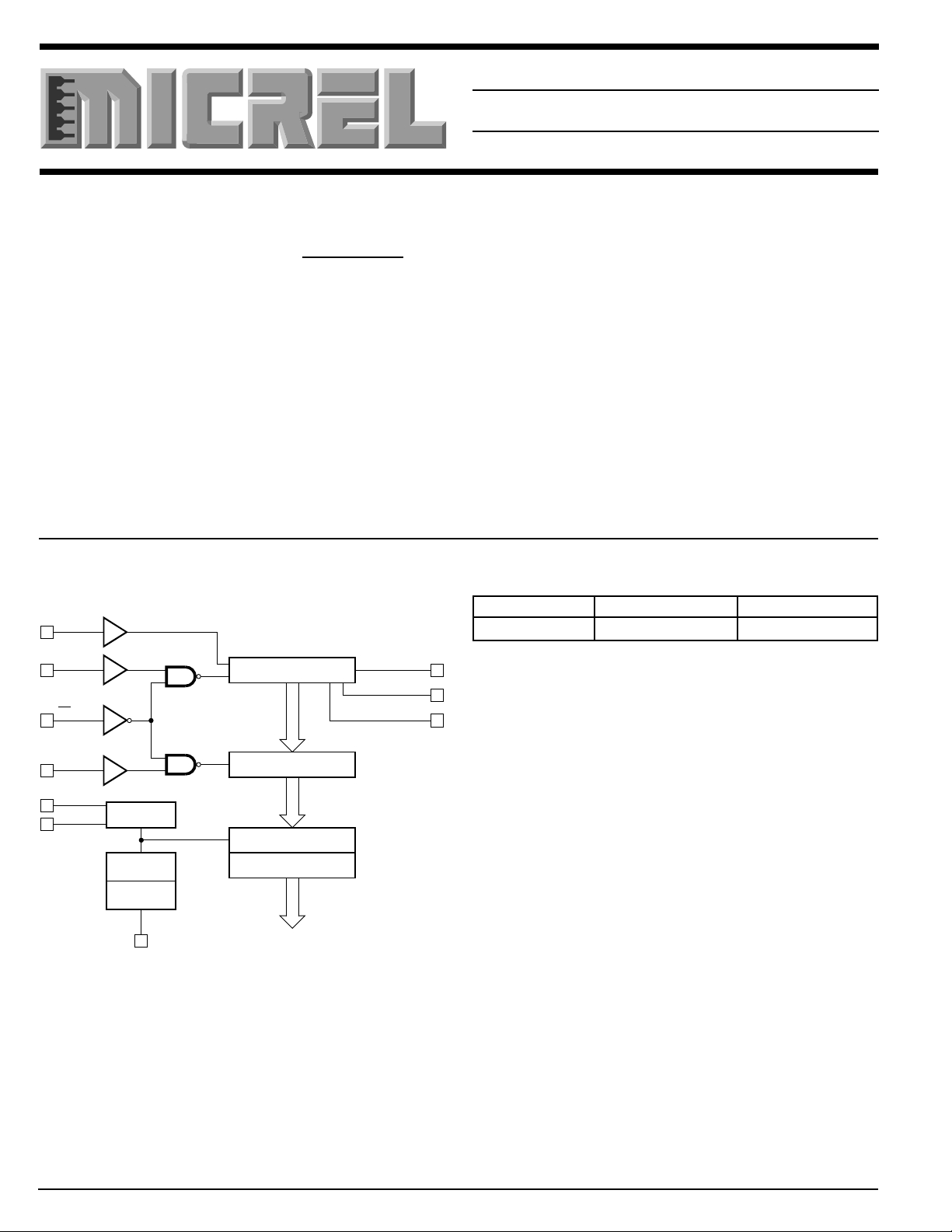
The MIC8030 is a CMOS high voltage liquid crystal display
driver. Up to 38 segments can be driven from four CMOS level
inputs (CLOCK, DATA IN, LOAD and CHIP SELECT). The
MIC8030 is rated at 50V. Data is loaded serially into a shift
register, and transferred to latches which hold the data until
new data is received.
The backplane can be driven from external source, or the
internal oscillator can be used. If the internal oscillator is
used, the frequency of the backplane will be determined by an
external resistor and capacitor. The oscillator need not be
used if a DC output is desired.
Functional Diagram
Data
S
Features
• High Voltage Outputs capable of a driving up to 100 volt
outputs from 5 to 15 volt logic
• Drives 30, 32, or 38 segments
• Cascadable
• On chip Oscillator or External Backplane Input
• CMOS construction for wide supply range and low
power consumption
• Schmitt Triggers on all inputs
• CMOS, PMOS, and NMOS compatible
Applications
• Dichroic and Standard Liquid Crystal Displays
• Flat Panel Displays
• Print Head Drives
• Vacuum Fluorescent Displays
Ordering Information
Part Number Temperature Range Package
MIC8030-01CV 0°C to +70°C 44-pin PLCC
Clock
CS
Load
LCD0
LCD0 Opt
S
S
S
Oscillator
Voltage
Translator
HV Output
Driver
Back Plane
38 Bit Static Shift Register
38 Bit Latch
Voltage Translators
HV Output Drivers
Segments
Data Out 38
Data Out 32
Data Out 30
MIC8030 8-16 October 1998
Page 2
MIC8030 Micrel
1
2
3
4
5
6
7
444342
41
8
Seg 20
MIC8030-01
9
10
11
12
13
14
15
16
17
18192021222324
4028
27
26
25
Chip Select
Data In
LCD
LCD Opt.
Seg 2
Seg 3
Seg 21
Seg 22
Seg 23
Seg 24
Seg 25
Seg 28
Seg 29
Seg 30
Seg 31
Seg 32
SS
V
CC
V
Data Out 32
Back Plate
Seg 17
Seg 16
Seg 15
Seg 14
Seg 13
Seg 12
Seg 11
Seg 10
Seg 9
Seg 8
Seg 7
Seg 6
Seg 5
Seg 4
BB
V
Seg 19
N/C
Seg 18
39
38
37
36
35
34
33
32
31
30
29
Seg 1
Clock
Load
Seg 27
Seg 26
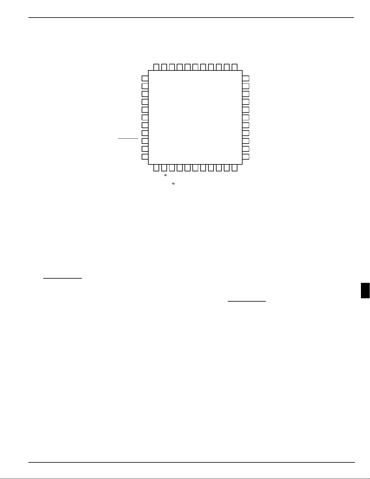
Pin Configuration
44-Pin PLCC (-V)
Functional Description
With CHIP SELECT tied low, serial data is clocked into the
shift register at each falling edge of the CLOCK input. Pulling
LOAD high will cause a parallel loading of the shift register
contents into the latches. If load is left high, the latches are
transparent.
A logic “1” clocked into the shift register corresponds to that
segment being on, and that segment is out of phase with the
backplane.
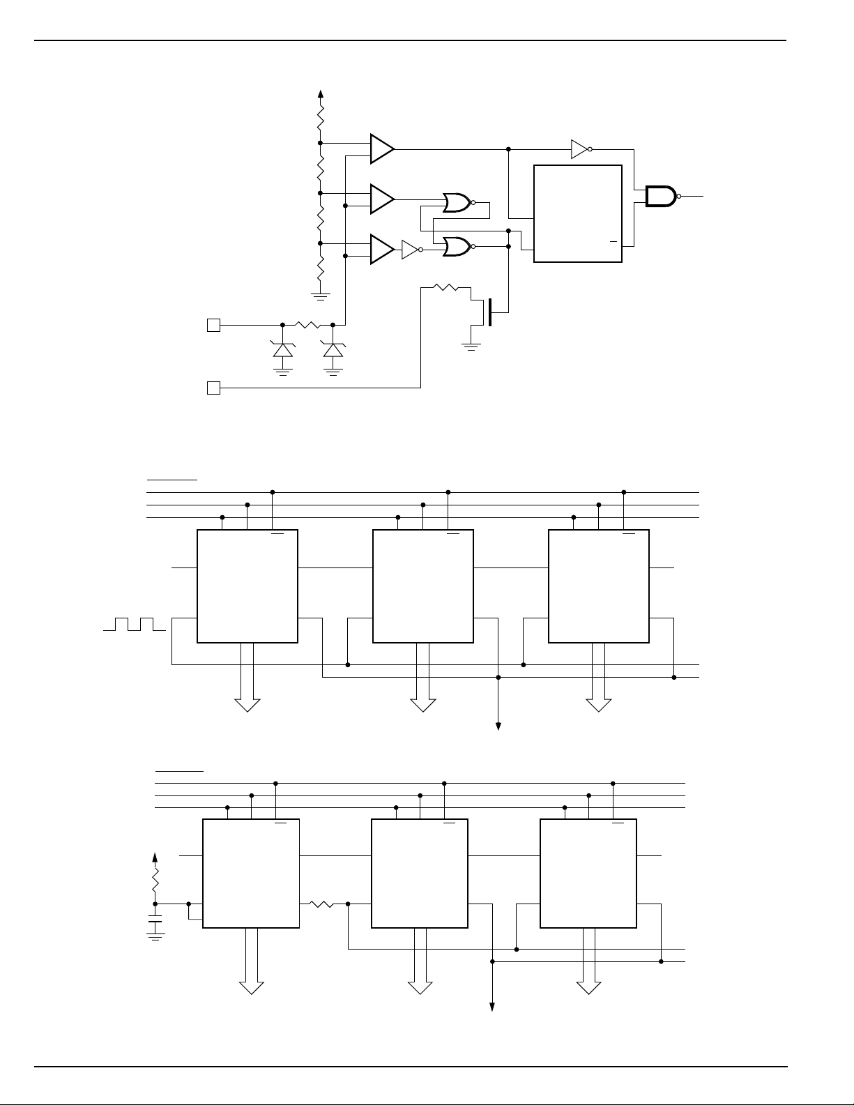
The backplane may be externally driven or the internal
oscillator can be used. If LCDφ is externally driven, the
backplane will be in phase with the input; LCDφ OPT is not
connected. The internal oscillator is used by shorting LCDφ
OPT to LCDφ, connecting a capacitor to ground, and a
resistor to VCC. The frequency of the backplane will be 1/256
of the input frequency, and is given as: f = 10/[R(C + .0002)]
at VDD = 5V, R in kΩ, C in µF.
Example: R = 150 kΩ, C = 420 pF: f = 108 Hz
For displays with more than 38 segments, two or more
MIC8030 may be cascaded by connecting DATA OUT of the
previous stage with DATA IN of the next stage; CLOCK,
LOAD and CHIP SELECT of all following stages should be
tied to the control lines of the first MIC8030. The backplane
output of the first stage should be tied to LCDφ of all following
stages, the LCDφ OPT must be left unconnected on those
stages. If the internal oscillator is used, and VBB > 50V then
an external 330 kΩ resistor must be used between the
BACKPLANE of the first stage and LCDφ of all following
stages.
Packaging options available include DATA OUT 30, 32 or 38
with the corresponding number of segments, and the availability of LCDφ OPT. Types of packages include plastic and
ceramic DIPs, surface mount packages, plastic and ceramic
Leadless Chip Carriers and custom packaging.
8
October 1998 8-17 MIC8030
Page 3
MIC8030 Micrel
Internal Oscillator Circuit
V
CC
200kΩ
–
+
200kΩ
200kΩ
Divide by
–
+
Counter
Reset
256
Q
O
Typical Application
External Oscillator
Chip Select
Clock
Load
Data
LCD0
V
Z
65V
LCD0 Opt
Load Clock CS
Data In
LCD0
Data Out
MIC8030
200kΩ
BP
30
kΩ
V
35V
–
+
Z
Data In
LCD0
1kΩ
Load Clock CS
Data Out
MIC8030
BP
Clock
Load Clock CS
Data In
MIC8030
LCD0
Q
Data Out
BP
Segments
1-32
Segments
33-64
Back Plane
Segments
65-96
Internal Oscillator
Chip Select
Clock
Load
Load Clock CS
Data
Data In
150kΩ
LCD0
470pF
*Required if using MIC8031 with V > 50V.
LCD0 Opt
Data Out
MIC8030
Segments
1-32
*330kΩ
BP
BB
Load Clock CS
Data In
LCD0
Data Out
MIC8030
Segments
33-64
BP
Back Plane
Load Clock CS
Data In
LCD0
Data Out
MIC8030
Segments
65-96
BP
MIC8030 8-18 October 1998
Page 4
MIC8030 Micrel
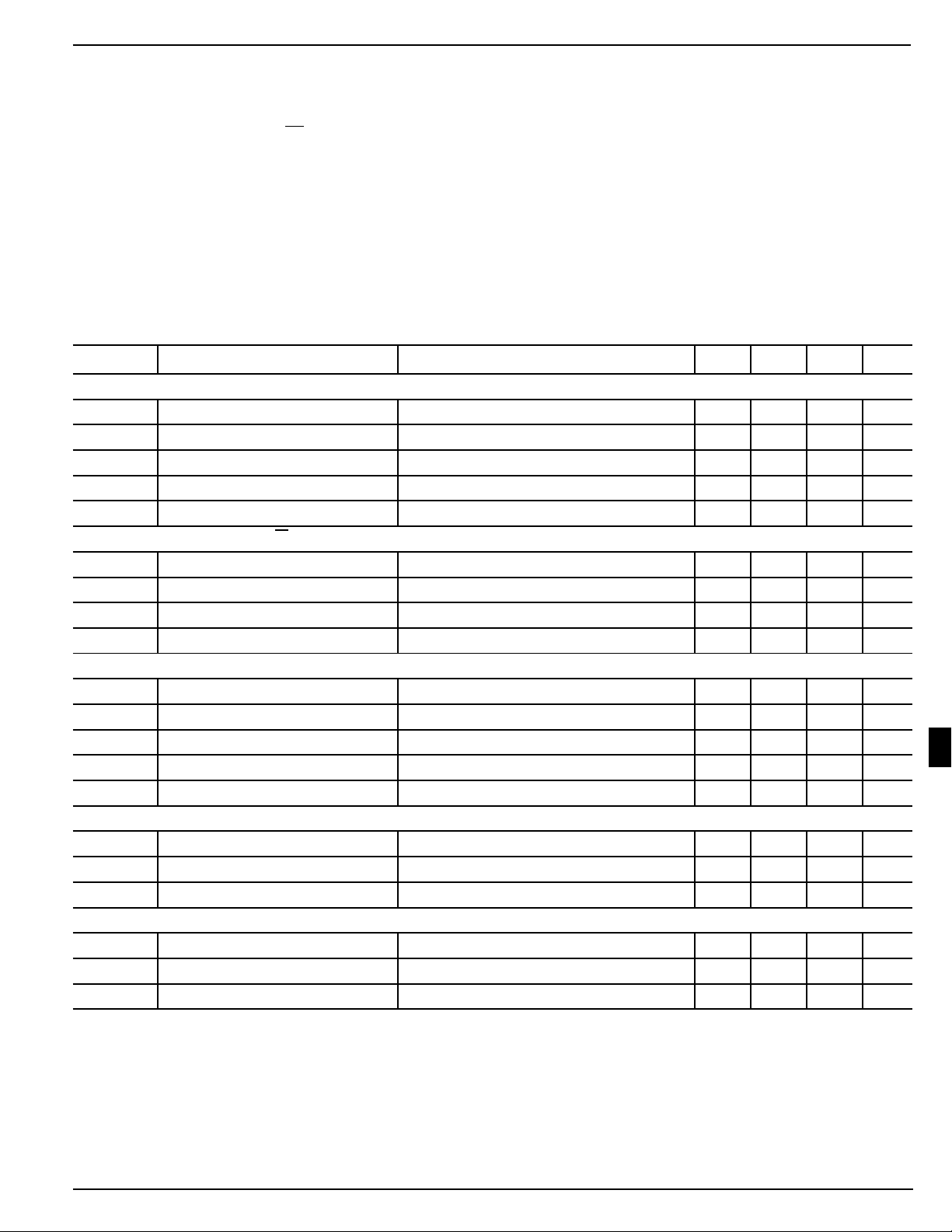
Absolute Maximum Ratings
V
CC
18V
VBB (MIC8030) 75V
Inputs (CLK, DATA IN, LOAD, CS) –0.5V to 18V
Inputs (LCD0) –0.5V to 50V
Storage Temperature –65°C to +150°C
Operating Temperature –55°C to +125°C
Maximum Current into and out of
any segment 20 mA
Maximum Power Dissipation,
any segment 50 mW
Maximum Total power dissipation 600 mW
DC Electrical Characteristics: V
Symbol Parameter Condition Min Typ Max Units
Power Supply
V
CC
V
BB
I
CC
I
BB
Inputs (CLK, DATA IN, LOAD, CS)
V
IH
V
IL
I
L
C
I
Input LCD0
V
IH
V
IL
I
LCD0
I
LCD0
I
LCD0
Capacitance Loads (typical)
C
LSEG
C
LBP
V
OAVG
Output to Backplane
R
SEG
R
BP
R
DATA OUT
Note 1: CMOS input levels. No loads.
Note 2: Guaranteed by design but not tested on a production basis.
Logic Supply Voltage 4.5 5 5.5 V
Display Supply Voltage 20 35 50 V
Supply Current (external oscillator) Note 1 35 250 µA
Supply Current (internal oscillator) Note 1 35 250 µA
Display Driver Current fBP = 100Hz, no loads 7 100 µA
Input High Level VCC-1.5 VCC-1.8 V
Input Low Level 0 2.5 2.0 V
Input Leakage Current <1 5 µA
Input Capacitance Note 2 510pF
LCD0 Input High Level Externally driven 0.9V
LCD0 Input Low Level Externally driven –0.5V 0 0.1V
LCD0 Leakage Current V
LCD0 Leakage Current V
LCD0 Leakage Current V
Segment Output fBP < 100Hz 100 pF
Backplane Output fBP < 100Hz 4000 pF
DC Bias (Average) Any Segment fBP < 100Hz, Note 2 +25 mV
Segment Output Impedance I
Backplane Output Impedance I
Data Out Output Impedance I
= 5V, VSS = 0V, VBB = 50V, –55°C ≤ TA ≤ +125°C, unless otherwise noted.
CC
CC
CCVCC
= 15V 2 10 µA
LCD0
= 35V 6 100 µA
LCD0
= 50V 1 mA
LCD0
= 100µA 1.4 10 kΩ
L
= 100µA 170 312 Ω
L
= 100µA 1.8 3 kΩ
L
50 V
CC
V
V
8
October 1998 8-19 MIC8030
Page 5
MIC8030 Micrel
AC Electrical Characteristics: V
Symbol Parameter Min Typ Max Units
t
CYC
tOL, tOH Clock Pulse Width low/high 250 ns
tr, t
f
t
DS
t
CSC
t
DH
t
CCS
t
CL
t
LCS
t
LW
t
LC
t
CDO
t
CSL
F
BP
Cycle Time 500 ns
Clock rise/fall 1 µs
Data In Setup 100 ns
CS Setup to Clock 100 ns
Data Hold 10 ns
CS Hold 220 ns
Load Pulse Setup 250 ns
CS Hold (rising load to rising CS) 200 ns
Load Pulse Width 300 ns
Load Pulse Delay (falling load to 0 ns
falling clock)
Data Out Valid from Clock 220 ns
CS Setup to LOAD 0 ns
Backplane Frequency 50 100 2000 Hz
= 5V, VSS = 0V, VBB = 50V, –55°C ≤ TA ≤ +125°C
CC
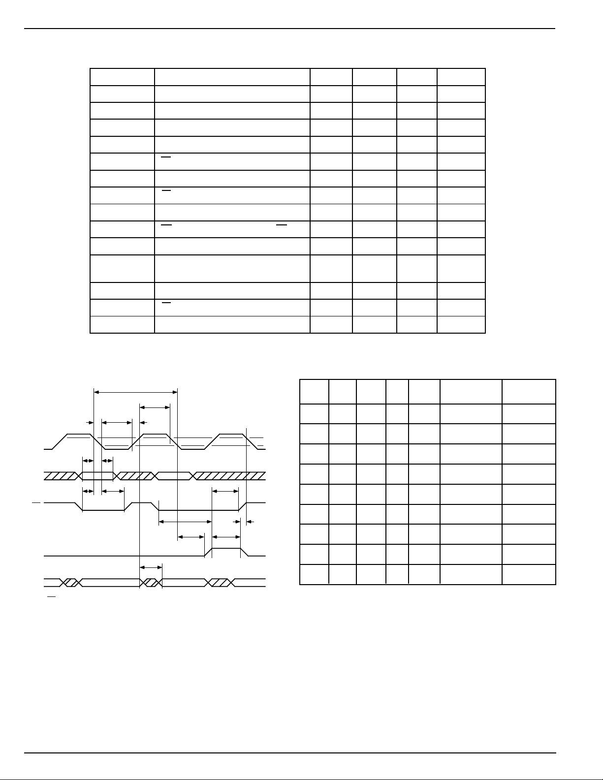
Timing Diagram
t
CYC
t
OH
t
OL
t
f
Clock
t
CCS
t
DH
t
Data
In
CS
Load
Data
Out
* The CS high-to-low transition will generate a clock pulse.
DS
t
CSC
**
t
CDO
t
r
t
CSL
Logic T ruth T able
Data Chip
In Clock Select Load Q
1(SR)
X X 1 X NC NC Q
3.5V
1.5V
0 ↑ 0 0 NC NC Q
0 ↑ 0 1 NC NC Q
0 ↓ 000QN - 1→Q
t
LCS
0 ↓ 010QN - 1→Q
t
t
CL
LC
t
LW
1 ↑ 0 0 NC NC Q
1 ↑ 0 1 NC NC Q
1 ↓ 001QN - 1→Q
1 ↓ 011QN - 1→Q
↑ = Rising Edge, ↓ = Falling Edge
Q
N(SR)
N
N
N
N
Q
N(DRIVER)
N(L)
N(L)
N(L)
Q
N(L)
Q
N(SR)
N(L)
N(L)
Q
N(L)
Q
N(SR)
MIC8030 8-20 October 1998
 Loading...