

Page 1
1
The MIC811/MIC812 are inexpensive microprocessor
supervisory circuits that monitor power supplies in
microprocessor based systems.
The function of these devices is to assert a reset if
either the power supply drops below a designated reset
threshold level or MR is forced low. Several different
reset threshold levels are available to accomodate 3V,
3.3V or 5V powered systems.
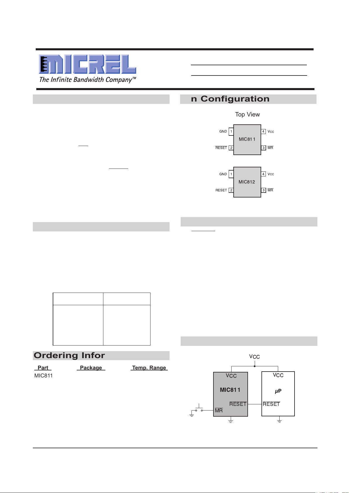
The MIC811 has an active low RESET output, while the
MIC812 offers an active high RESET output. The reset
output is guaranteed to remain asserted for a minimum
of 140ms after VCChas risen above the designated
reset threshold level. The MIC811/MIC812 come in a 4pin SOT-143 package.
1
2
4 V
CC
GND
MIC812
RESET 3
MR
1
2
4
V
CC
GND
MIC811
RESET 3
MR
Top View
Part Package Temp. Range
MIC811_U 4-Lead SOT-143 -40°C to +85°C
MIC812_U 4-Lead SOT-143 -40°C to +85°C
Place the device suffix of desired reset threshold voltage from table above in
blank to complete the part number.
·
Portable Equipment
·
Intelligent Instruments
·
Critical Microprocessor Power Monitoring
·
Printers/Computers
·
Controllers
·
RESET Remains Valid with V
CC
as Low
as 1.4V
·
Precision Voltage Monitor for 3V, 3.3V
or 5V Power Supplies
·
Available in 4-Pin SOT-143 Package
·
<15µA Supply Current
·
140ms Minimum Reset Pulse Width
·
Manual Reset Input
V
CC
RESET
µP
RESET
V
CC
MIC811
V
CC
MR
Typical Operating Circuit
Features
Description Pin Configuration
Ordering Information
Typical Applications
Reset Threshold Device
Voltage (V) Suffix
4.63 L
4.38 M
4.00 J
3.08 T
2.93 S
2.63 R
MIC811/MIC812 Microprocessor Reset Circuits
MIC811/MIC812
Microprocessor Reset Circuits
Page 2
MIC811/MIC812 Microprocessor Reset Circuits
2
Electrical Characteristics
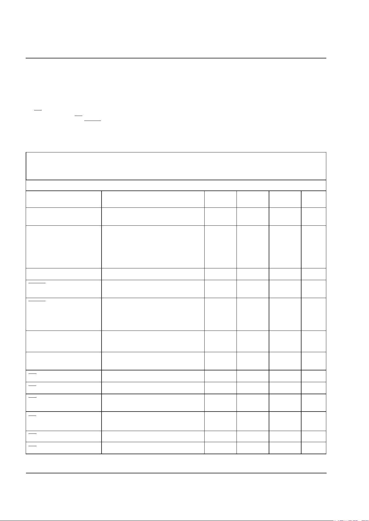
VCC= 5V for MIC81-L/M/J, VCC= 3.3V for MIC81-S/T, VCC= 3V for MIC81-R, TA= Operating Temperature Range, unless
otherwise noted.
Parameter Conditions Min Typ Max Units
Operating Voltage Range, V
CC
TA= 0°C to 70°C 1.4 5.5 V
TA= -40°C to 85°C 1.6 5.5
Supply Current, I
CC
MIC811L/M/J, MIC812L/M/J 9 15 µA
VCC< 3.6V, MIC811R/S/T, MIC812R/S/T 6 10
Reset Voltage Threshold, V
TH
MIC811L, MIC812L 4.50 4.63 4.75 V
MIC811M, MIC812M 4.25 4.38 4.50
MIC811J, MIC812J 3.89 4.00 4.10
MIC811T, MIC812T 3.00 3.08 3.15
MIC811S, MIC812S 2.85 2.93 3.00
MIC811R, MIC812R 2.55 2.63 2.70
Reset Timeout Period 140 240 560 ms
RESET Output Voltage, V
OH
I
Source
= 800µA, MIC811L/M/J
VCC- 1.5V
V
I
Source
= 500µA, MIC811R/S/T 0.8 X
V
CC
RESET Output Voltage, V
OL
VCC=VTHMin., I
Sink
=3.2mA, MIC811L/M/J
0.4 V
VCC=VTHMin., I
Sink
=1.2mA, MIC811R/S/T
0.3
VCC>1.4V, I
Sink
=50µA,
TA= 0°C to 70°C 0.3
VCC>1.6V, I
Sink
=50µA,
TA= -40°C to 85°C 0.3
RESET Output Voltage, V
OH
1.8V < V
CC
< VTHMin., 0.8 X
V
CC
V
I
Source
= 150µA
RESET Output Voltage, V
OL
I
Sink
=3.2mA, MIC812L/M/J 0.4 V
I
Sink
=1.2mA, MIC812R/S/T 0.3
MR Minimum Pulse Width 10 µs
MR to Reset Delay 0.5 µs
MR Input Threshold, V
IH
VCC>
VTHMax., MIC81_L/M/J 2.3 V
MIC81_R/S/T 0.7 X
V
CC
MR Input Threshold, V
IL
VCC>
VTHMax., MIC81_L/M_ 0.8 V
MIC81_R/S/T 0.25 X
V
CC
MR Pull-Up Resistance
10 20 30 kΩ
MR Glitch Immunity
100 ns
Absolute Maximum Ratings
Terminal Voltage
VCC. . . . . . . . . . . . . . . . . . . . . . . . . . . -0.3V to 6.0V
MR . . . . . . . . . . . . . . . . . . . . . -0.3V to (VCC+ 0.3V)
Input Current, VCC, MR . . . . . . . . . . . . . . . . . . . . 20mA
Output Current, RESET, RESET . . . . . . . . . . . . . .20mA
Rate of Rise, V
CC
. . . . . . . . . . . . . . . . . . . . . . 100V/µs
Operating Temperature Range
MIC81
--
U . . . . . . . . . . . . . . . . . . . . . . . . -40°C to 85°C
Storage Temperature Range . . . . . . . . . . . . . -65°C to 150°C
Lead Temperature (Soldering - 10 sec.) . . . . . . . . . . . 300°C
Power Dissipation (TA= +70°C) . . . . . . . . . . . . . . . . 320mW
Stresses above those listed under ABSOLUTE MAXIMUM RATINGS may cause permanent device failure. Functionality at or above these limits is not implied. Exposure to absolute
maximum ratings for extended periods may affect device reliability. Operating ranges define those limits between which the functionality of the device is guaranteed.
Page 3

Pin Functions
Description
IC Ground Pin.
RESET goes low if VCCfalls below the reset threshold and remains
asserted for one reset timeout period (140ms min.) after VCCexceeds
the reset threshold.
RESET goes high if VCCfalls below the reset threshold and remains
asserted for one reset timeout period (140ms min.) after VCCexceeds
the reset threshold.
Manual reset input. A logic low on MR forces a reset. The reset will
remain asserted as long as MR is held low and for one reset timeout
period (140ms min.) after MR goes high. This input can be shorted to
ground via a switch or driven from CMOS or TTL logic. Float if unused.
Power supply input, 3V, 3.3V or 5V.
Pin No.
Pin Name MIC811 MIC812
GND 11
RESET 2 N/A
RESET N/A 2
MR 33
V
CC
44
MIC811/MIC812 Microprocessor Reset Circuits
3
Page 4
MIC811/MIC812 Microprocessor Reset Circuits
4
+
-
Reset
Threshold (V)
VCC(4)
RESET (2)
RESET (MIC812)
GND (1)
RESET
GENERATOR
MR (3)
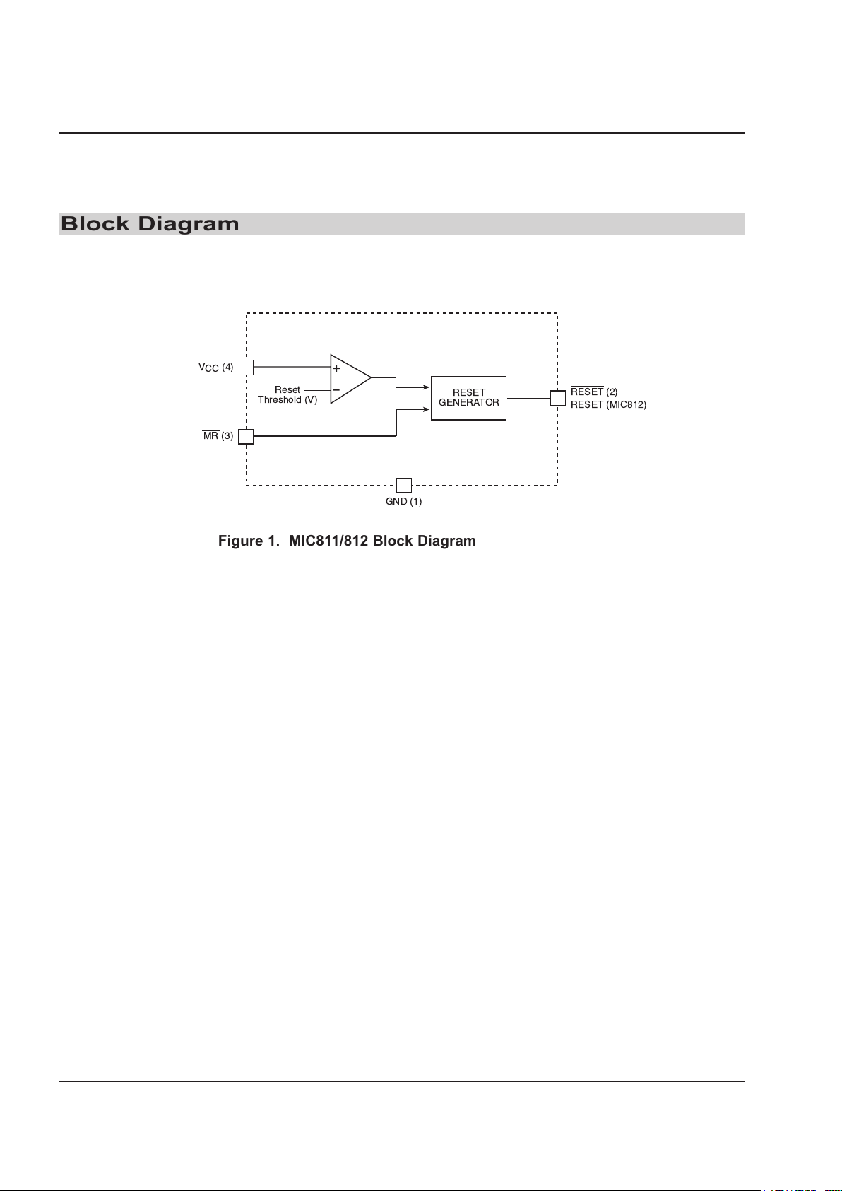
Figure 1. MIC811/812 Block Diagram
Block Diagram
Page 5
Microprocessor Reset
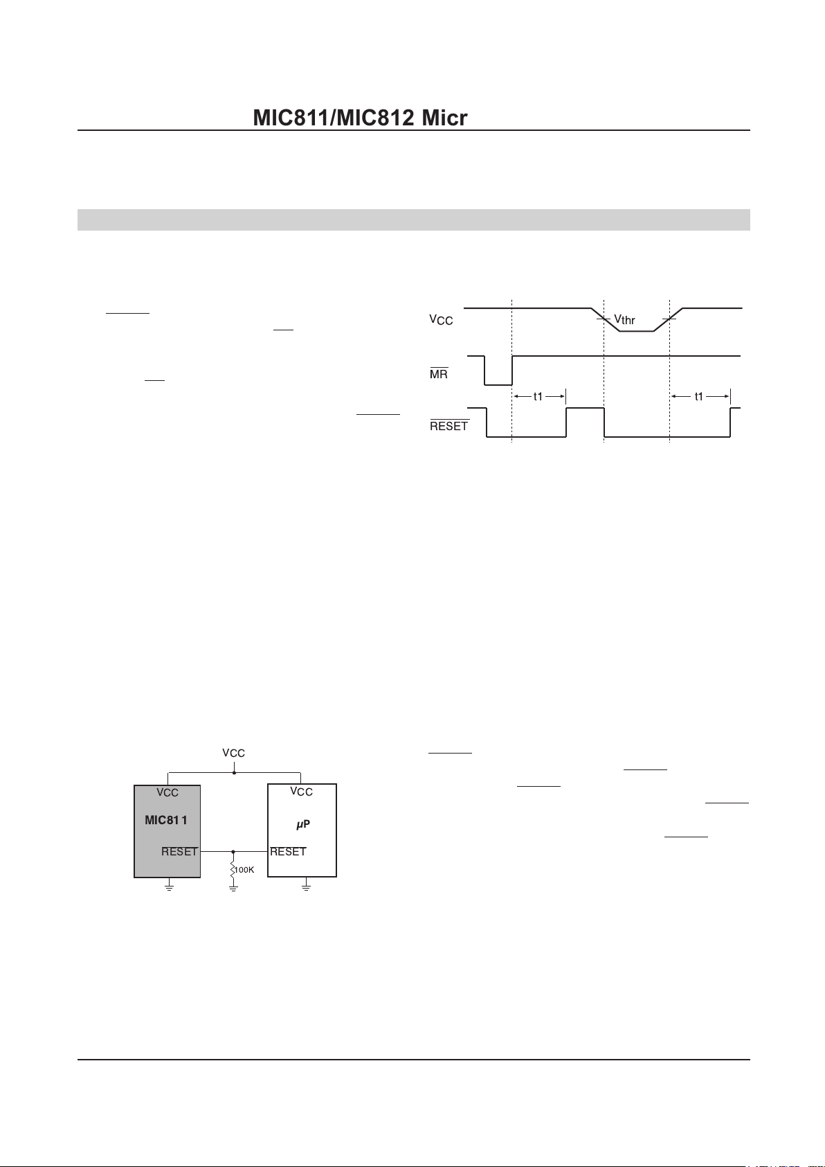
The RESET pin is asserted whenever V
CC
falls below
the reset threshold voltage or if MR (manual reset) is
forced low. The reset pin remains asserted for a period
of 240ms after VCChas risen above the reset threshold
voltage or MR has returned high. The reset function
ensures the microprocessor is properly reset and powers
up into a known condition after a power failure. RESET
will remain valid with VCCas low as 1.4V.
VCCTransients
The MIC811/MIC812 are relatively immune to negativegoing VCCglitches below the reset threshold. Typically,
a negative-going transient 125mV below the reset
threshold with a duration of 50µs (25µs for
MIC81_R/S/T) or less will not cause an unwanted reset.
Interfacing to Bidirectional Reset Pins
The MIC811/MIC812 can interface with µPs with
bidirectional reset pins by connecting a 4.7KΩ resistor in
series with the MIC811/MIC812 output and the µP reset
pin.
RESET Valid to 0V
A resistor can be added from the RESET pin to ground
to ensure the RESET output remains low with V
CC
down to 0V. A 100KΩ resistor connected from RESET
to ground is recommended. The size of the resistor
should be large enough to not load the RESET output
and small enough to pull-down any stray leakage
currents.
Circuit Description
Figure 2. Reset Timing Diagram
Figure 3. RESET Valid to VCC= 0V.
V
CC
MR
RESET
t1t1
V
thr
MIC811/MIC812 Microprocessor Reset Circuits
5
V
CC
RESET
µP
RESET
V
CC
MIC811
V
CC
100K
Page 6

MIC811/MIC812 Microprocessor Reset Circuits
6
MIC Direct
Industry P/N Replacement
MAX811JEUS-T MIC811JU
MAX811LEUS-T MIC811LU
MAX811MEUS-T MIC811MU
MAX811REUS-T MIC811RU
MAX811SEUS-T MIC811SU
MAX811TEUS-T MIC811TU
MAX812JEUS-T MIC812JU
MAX812LEUS-T MIC812LU
MAX812MEUS-T MIC812MU
MAX812REUS-T MIC812RU
MAX812SEUS-T MIC812SU
MAX812TEUS-T MIC812TU
Alternate Source Cross Reference Guide
Page 7
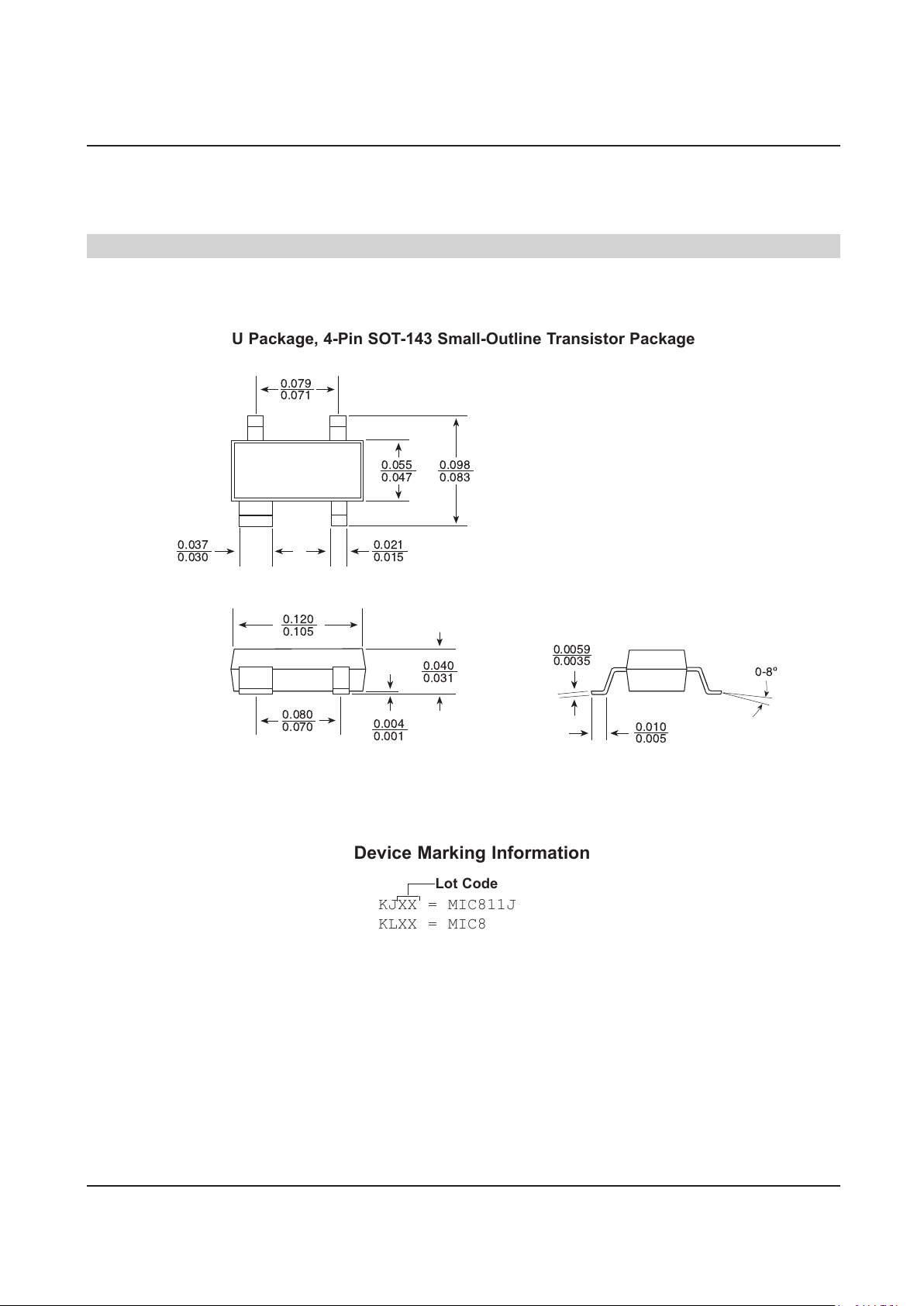
Packaging Information
0.0059
0.0035
0.010
0.005
0-8¼
0.080
0.070
0.120
0.105
0.040
0.031
0.004
0.001
0.021
0.015
0.055
0.047
0.098
0.083
0.079
0.071
0.037
0.030
U Package, 4-Pin SOT-143 Small-Outline Transistor Package
Device Marking Information
Lot Code
KJXX = MIC811J
KLXX = MIC811L
KMXX = MIC811M
KRXX = MIC811R
KSXX = MIC811S
KTXX = MIC811T
LJXX = MIC812J
LLXX = MIC812L
LMXX = MIC812M
LRXX = MIC812R
LSXX = MIC812S
LTXX = MIC812T
Dimensions are in inches.
MIC811/MIC812 Microprocessor Reset Circuits
7
Page 8
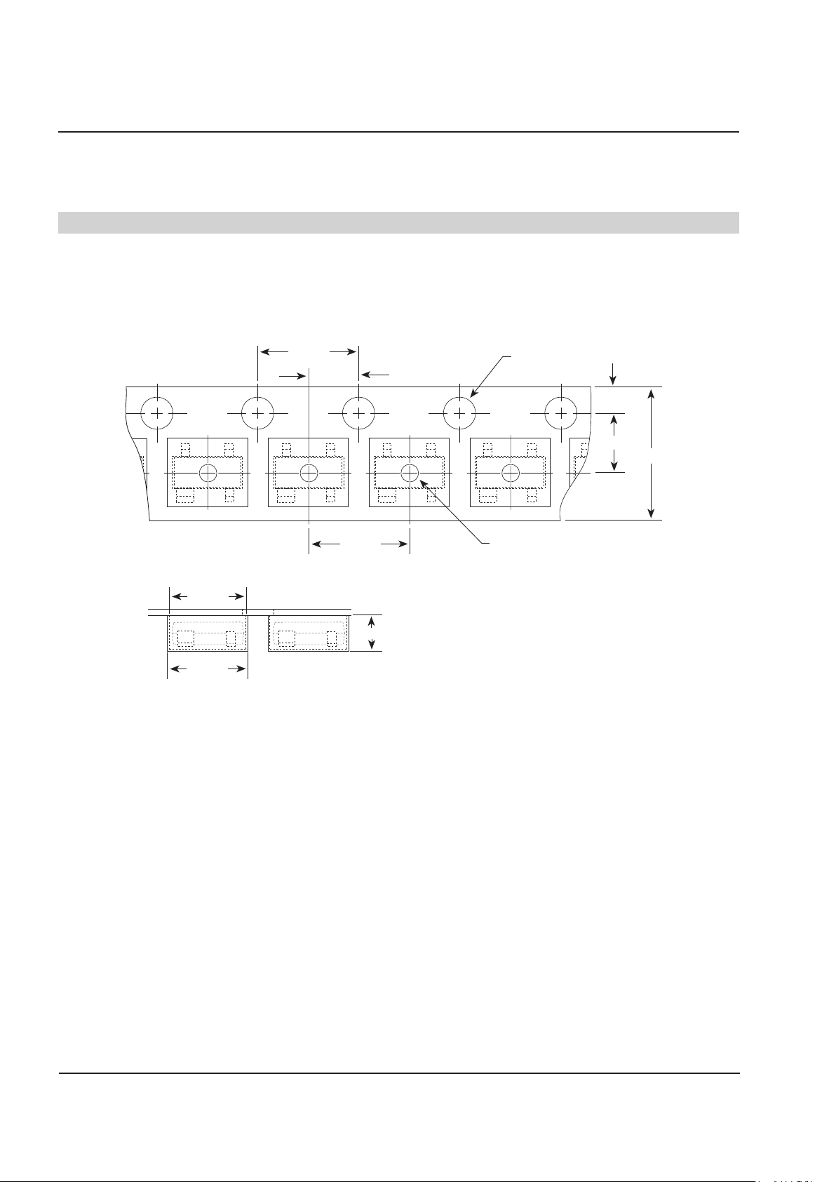
MIC811/MIC812 Microprocessor Reset Circuits
8
Packaging Information
4.0–0.1
4.0–0.1
2.0–0.05
3.5–0.05
8.0–0.3
1.75–0.1
fl1.5–0.1
fl1.1–0.1
2.7–0.1
3.1–0.1
1.2–0.1
Tape and Reel Information
Dimensions are in millimeters.
 Loading...