

Page 1

MICRF405
290MHz – 980MHz ISM Band
ASK / FSK Transmitter
General Description
The MICRF405 is a 290MHz-980MHz RF transmitter
IC designed for unlicensed ISM band operations. It's
designed to work in the North American 315MHz
and 915MHz bands as well as the European
433MHz and 868MHz bands. The device is fully
FCC Part 15.247 and EN300-220-compliant.
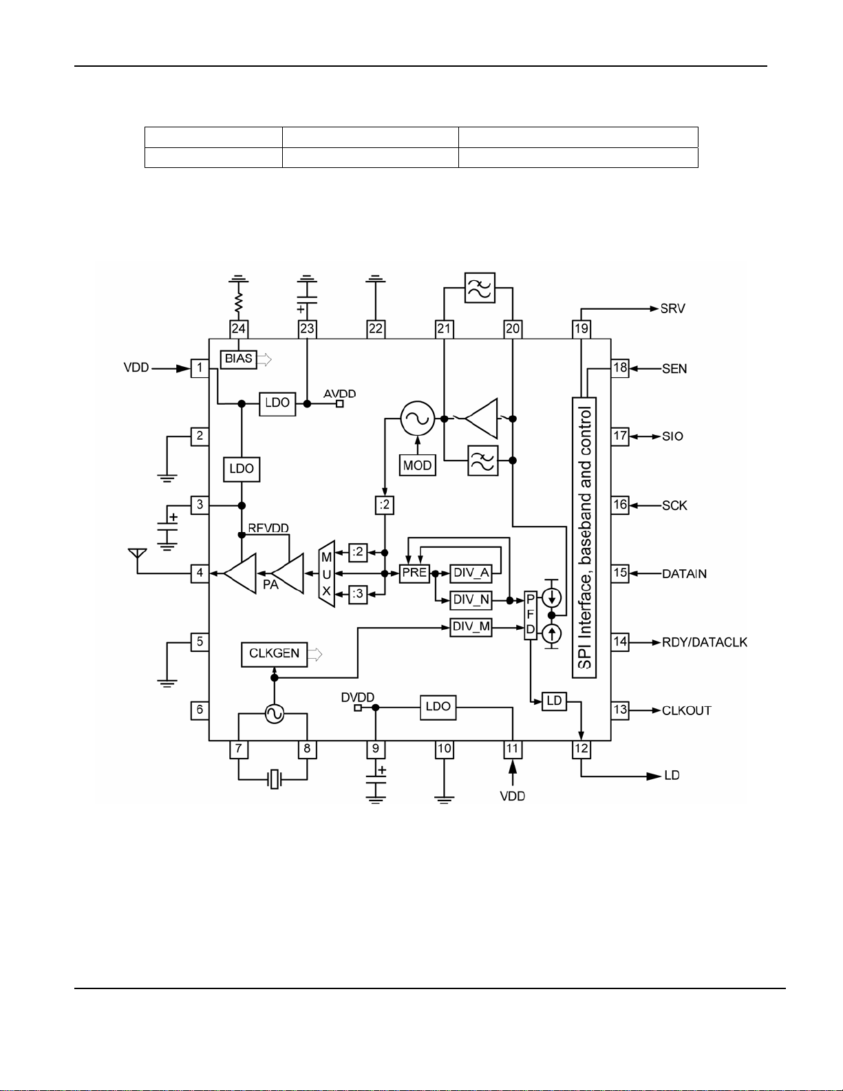
The transmitter consists of a FSK/ASK modulator,
PLL frequency synthesizer and a power amplifier.
The frequency synthesizer consists of a voltagecontrolled oscillator (VCO), a crystal oscillator, dual
modulus prescaler, programmable frequency
dividers and a phase-detector. The loop-filter can be
internal or external. The output power of the power
amplifier can be programmed to eight levels. A lock
detect circuit detects when the PLL is in lock.
In FSK mode, the user can select between three
different modulation types allowing a data rate up to
200kbps. When selecting FSK modulation applied
with dividers, the MICRF405 is switching between to
sets of register values (M0,N0,A0:"0" and M1,N1
and A1:"1"). The second modulation type is closed
loop VCO modulation using the internal modulator
that applies the modulated data to the VCO. The
third FSK modulation type is Open loop VCO
modulation.
In ASK modulation, the user can select between two
modulation types, with or without spreading. In both
modes the modulation depth is programmable.
RadioWire®
Features
• FSK/ASK transmitter
• Frequency programmable
• ASK modulation depth programmable
• High efficiency power amplifier
• Programmable output power
• Power down function
• MCU reference clock
• Base band package engine
• TX buffer
• No external tuning circuitry
Applications
• Meter reading
• Automotive
• Smart Home
• Remote control systems
• Residential Automation
• Wireless security system
MicroLead Frame and MLF are registered trademarks of Amkor Technologies
RadioWire is a registered trademark of Micrel, Inc.
Micrel Inc. • 2180 Fortune Drive • San Jose, CA 95131 • USA • tel +1 (408) 944-0800 • fax + 1 (408) 474-1000 • http://www.micrel.com
April 2006
M9999-041906
(408) 955-1690
Page 2

Micrel MICRF405
Table of Contents
General Description ................................................................................................................................................................... 1
Features..................................................................................................................................................................................... 1
Applications................................................................................................................................................................................ 1
Table of Contents....................................................................................................................................................................... 2
Ordering Information .................................................................................................................................................................. 3
Block Diagram............................................................................................................................................................................ 3
Pin Configuration........................................................................................................................................................................ 4
Absolute Maximum Ratings
Operating Ratings
Electrical Characteristics............................................................................................................................................................ 5
Electrical Characteristics (cont.)................................................................................................................................................. 6
Data and Configuration Interface ............................................................................................................................................... 7
Programming Interface Timing .............................................................................................................................................. 8
Writing to the Control Registers in MICRF405....................................................................................................................... 9
What to write: ........................................................................................................................................................................ 9
How to write:.......................................................................................................................................................................... 9
The two different ways to “program the chip” are: ................................................................................................................. 9
Writing to a Single Register................................................................................................................................................... 9
How to write:.......................................................................................................................................................................... 9
Writing to All Registers........................................................................................................................................................ 10
What to write ....................................................................................................................................................................... 10
How to write:........................................................................................................................................................................ 10
Writing to n Registers Having Incremental Addresses......................................................................................................... 10
What to write ....................................................................................................................................................................... 11
Writing to n Registers Having Non-Incremental Addresses................................................................................................. 12
Reading from the Control Registers in MICRF405 .............................................................................................................. 12
Reading from the Interrupt Register .................................................................................................................................... 12
Data Interface and Data Transfer............................................................................................................................................. 13
Packet Engine Overview: .................................................................................................................................................... 14
How to transmit a Packet with the Packet Engine: .............................................................................................................. 15
Programming Summary....................................................................................................................................................... 17
Main Modes of Operation......................................................................................................................................................... 18
Power Amplifier........................................................................................................................................................................ 18
Frequency Synthesizer............................................................................................................................................................. 19
Crystal Oscillator (XCO)........................................................................................................................................................... 21
VCO ......................................................................................................................................................................................... 22
Charge Pump and PLL Filter.................................................................................................................................................... 24
Modulation................................................................................................................................................................................ 27
Bit rate settings.................................................................................................................................................................... 30
Modulator ............................................................................................................................................................................ 30
Deviation setting.................................................................................................................................................................. 31
Shaping ............................................................................................................................................................................... 31
Modulator saturation............................................................................................................................................................ 31
Lock Detect ......................................................................................................................................................................... 32
Low Dropout Regulator (LDO) and Low Battery Detector.................................................................................................... 33
Bit Description.......................................................................................................................................................................... 34
Typical Application Circuit........................................................................................................................................................ 42
Package Information ................................................................................................................................................................ 45
(2)
(1)
..................................................................................................................................................... 5
................................................................................................................................................................... 5
April 2006
2
M9999-041906
(408) 955-1690
Page 3
Micrel MICRF405
Ordering Information
Part Number Junction Temp. Range
MICRF405YML –40° to +125°C PB-Free 24-Pin MLF®
____________________________________________________________________________________________________
(1)
Package
Block Diagram
April 2006
3
M9999-041906
(408) 955-1690
Page 4
Micrel MICRF405
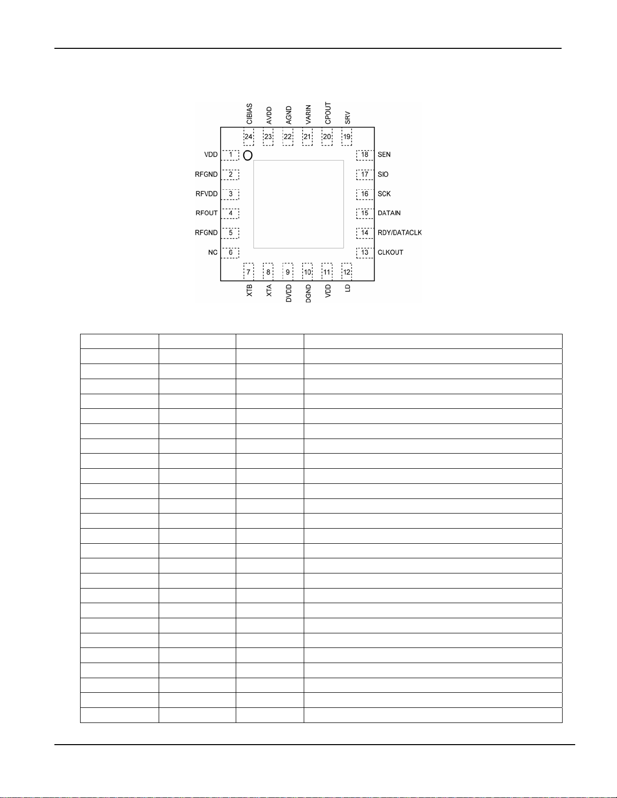
Pin Configuration
24-Pin MLF® (Top View)
Pin Number Pin Name Type Pin Function
1 VDD VDD
2 RFGND RF Ground
3 RFVDD RF VDD
4 RFOUT O RF output
5 RFGND RF Ground
6 NC Not connected
7 XTB O Crystal oscillator output
8 XTA I Crystal oscillator input
9 DVDD Digital VDD
10 DGND Digital ground
11 VDD VDD
12 LD O Lock Detect output
13 CLKOUT O Programmable Clock output
14 RDY/DATACLK O Transmit buffer Ready / Alternative Data clock
15 DATAIN I Alternative Data input
16 SCK I SPI clock
17 SIO I/O Serial input/output
18 SEN I Serial programming interface enable
19 SRV O Service interrupt pin
20 CPOUT O Charge pump output
21 VARIN I VCO varactor input
22 AGND Analog ground
23 AVDD Analog VDD
24 CIBIAS O Bias
25 HEATSINK Ground
April 2006
4
M9999-041906
(408) 955-1690
Page 5
Micrel MICRF405
Absolute Maximum Ratings
(1)
Operating Ratings
(2)
Supply Voltage (VDD)......................................... +3.7V
Voltage on any pin
(3)
(GND = 0V). .. -0.3V to 3.7V
Lead Temperature (soldering, 20sec.)............. 260°C
Storage Temperature (T
ESD Rating
(4)
) ................-55°C to +150°C
s
All pins except pin 4...................................... 2 kV
Supply voltage (VIN)............................ +2.2V to +3.6V
RF Frequencies.......................... 290MHz to 980MHz
Data Rate (NRZ) ...........................................200kbps
Ambient Temperature (T
Package Thermal Resistance
MLF
®
(ΘJA) ............................................41.7°C/W
) ..............–40°C to +125°C
A
Pin 4 (RFOUT)............................................ 200 V
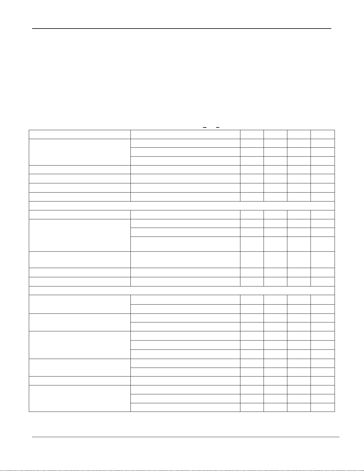
Electrical Characteristics
fRF = 915MHz. VDD = 3.0V; TA = 25°C, bold values indicate –40°C< TA < +125°C, unless noted.
Parameter Condition Min Typ Max Units
290
430
860
2.2
RF Frequency Operating Range
Power Supply
Power Down Current
Standby Current
Freq_band=0
Freq_band=1
Freq_band=2-3
0.3
ClkOut_en=0 200
PLL mode current PA2-0=000, PA off 5.6
VCO and PLL Section
Reference Frequency
4 40
1kHz loop filter bandwidth, Fphd=200kHz 7.0
PLL startup
3kHz loop filter bandwidth, Fphd=500kHz 1.8
30kHz loop filter bandwidth,
140
Fphd=1000kHz
Standby-TX (PA on)
200
30kHz bandwidth
Crystal Oscillator Start-Up Time
Charge Pump Current
16MHz, 9pF load, XCO_Fast=1 300
V
= 1.2V, CP_CUR = 3
CPOUT
100
Transmit Section
Output Power
Output Power Tolerance
Modulation depth ASK/OOK
Binary FSK Frequency Deviation
Data Rate
(5)
R
= 250Ω, Pa2-0=111
LOAD
= 250Ω, Pa2-0=001
R
LOAD
Over temperature range 1.5 dB
Over power supply range 3.0 dB
R
= 150Ω, PA2-0=111
LOAD
R
= 150Ω, PA2-0=001
LOAD
R
= 150Ω, PA2-0=000
LOAD
ASK=7 (OOK)
ASK=6
(5)
Bitrate = 200kbps
VCO modulation
Divider modulation
ASK
10 dBm
-7 dBm
18 mA
9.6 mA Tx Current Consumption
5.6 mA
60
20
300
20 200
20
50
325
490
980
3.6
MHz
MHz
MHz
V
µA
µA
mA
MHz
ms
ms
µs
µs
µs
µA
dB
dB
kHz
kbps
kbps
kbps
April 2006
5
M9999-041906
(408) 955-1690
Page 6
Micrel MICRF405
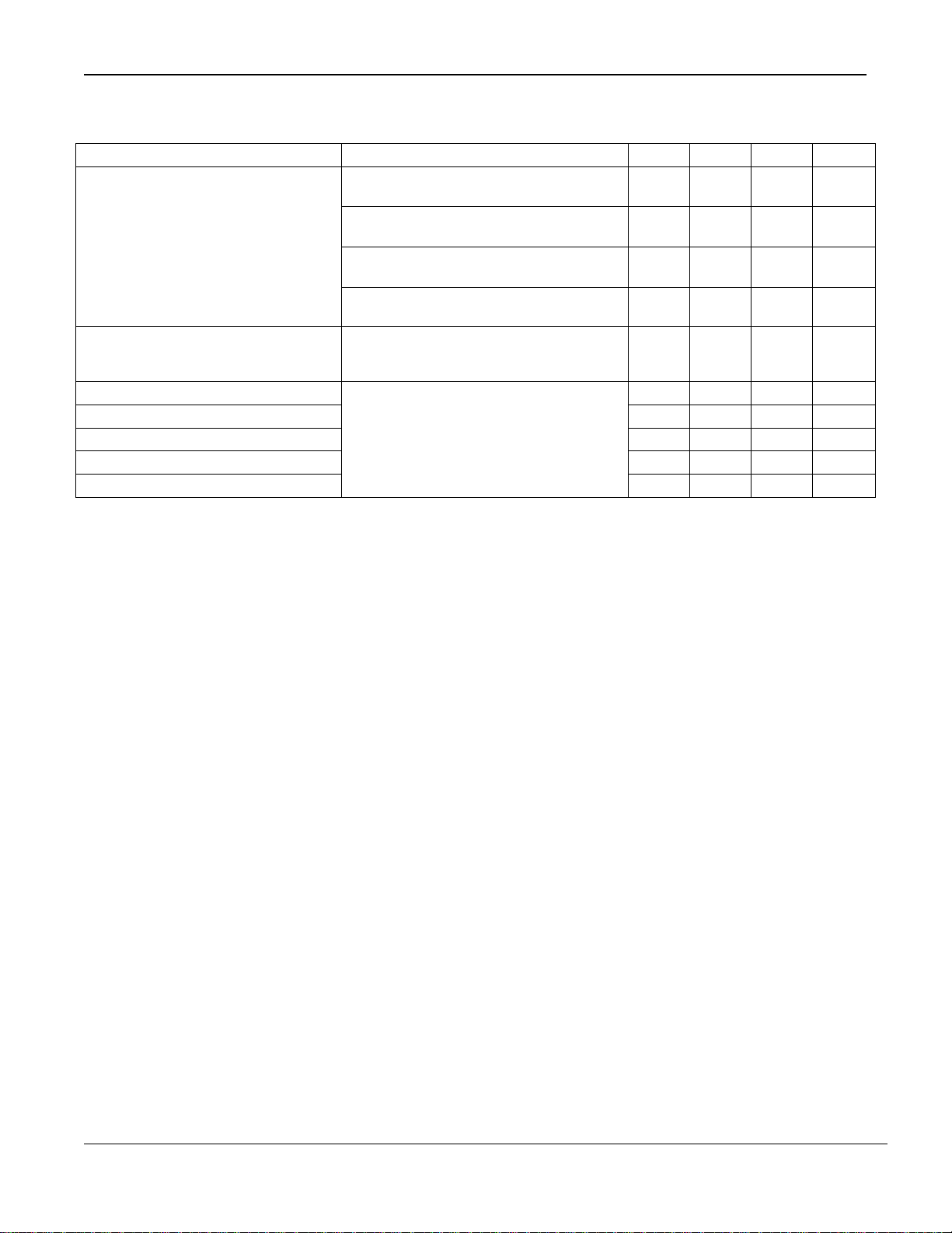
Electrical Characteristics (cont.)
Parameter Condition Min Typ Max Units
FSK 38.4kbps, β = 2, bandwidth for 99.5%
of total power, RBW=10kHz
FSK 125kbps, β = 2, bandwidth for 99.5%
Occupied bandwidth
of total power, RBW=30kHz
FSK 200kbps, β = 2, bandwidth for 99.5%
of total power, RBW=100kHz
ASK (OOK) 38.4kbps, bandwidth for 99.5%
of total power, RBW=10kHz
ASK 20dB modulation depth, 38.4kbps,
bandwidth for 99% of total power,
RBW=10kHz
nd
2
Harmonic -36 dBm
3rd Harmonic -54 dBm
Spurious Emission<1GHz -54 dBm
Measured with matching network
Spurious Emission>1GHz -41 dBm
LO Leakage
Notes:
1. Exceeding the absolute maximum rating may damage the device.
2. The device is not guaranteed to function outside its operating rating.
3. On the pins RFVDD (3), PTATBIAS (6), DVDD (9), CPOUT (20), VARIN (21) and AVDD (23), the maximum input voltage should not
exceed 2.75V.
4. Devices are ESD sensitive. Handling precautions recommended. Pin 4, RFOUT, has less ESD protection (Human body model (HBM) of
200V and Charged Device Model (CDM) of 500V).
5. Guaranteed by design.
130 kHz
425 kHz
750 kHz
200 kHz
120 kHz
-80 dBm
April 2006
6
M9999-041906
(408) 955-1690
Page 7
Micrel MICRF405
Data and Configuration Interface
desktop register controlling the state of the 405, the
PA and clock-out for the microcontroller. The next
The user interface of the MICRF405 is a serial
peripheral interface (SPI) consisting of Serial
interface enable (SEN), Serial data input/output
(SIO) and Serial clock (SCK). This user interface is
used for MICRF405 configuration setup and can
also be used for sending the user data. A second
option is to transmit data bitwise using the DATAIN
pin. The RDY/DATACLK pin is used to synchronize
the data transfers.
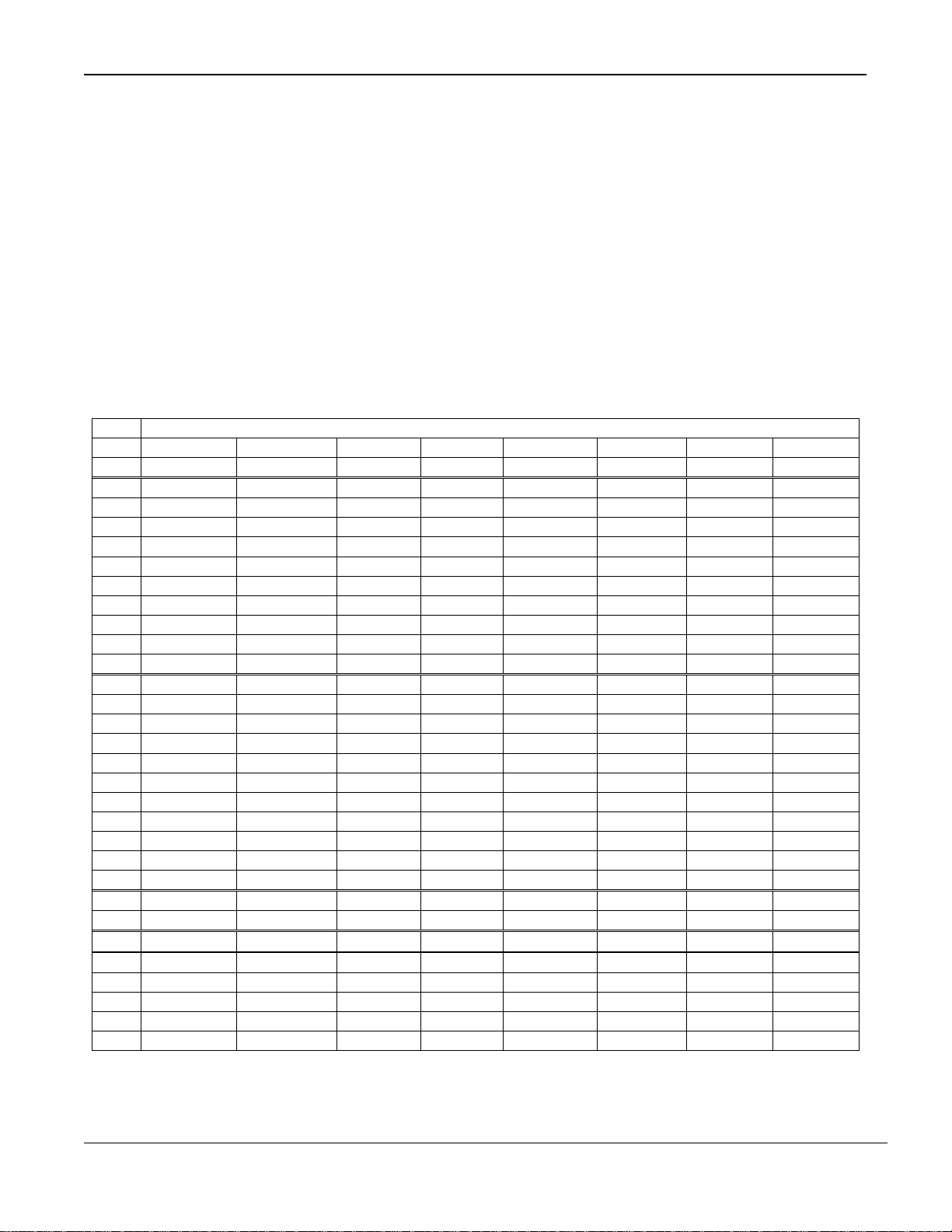
The control word consists of 30 addressable bytes
and defines the way of operations as well as
transmitting data. Table 1 shows all 30 bytes. The
values specified are the default setup, which are
preset after power up. The first register is the
block of 10bytes sets the output radio frequency
through the dividers A, N and M. The bytes with
address 11 to 21 set the frequency band, modulation
type, bit rate, loop filter type and bandwidth, XCO
tuning etc. This block is not frequently used as these
settings are usually static application dependent.
Address 22 and 23 are mostly test bits, and are
seldom altered from default settings in applications.
The interrupt register, which is located at address
24, is read only (writing to it will not do any harm or
have any effect). The last 5 bytes are used when
transferring user data to transmit through the SPI.
The first four set the SyncID field in the packet, and
the last is the one byte data buffer.
Adr Data
A6..A0 D7 D6 D5 D4 D3 D2 D1 D0
0000000 Mode1=0 Mode0=1 PA2=1 PA1=1 PA0=1 ClkOut_en=1 Sync_en=1 Load_en=1
0000001 - - A0_5=0 A0_4= 0 A0_3=1 A0_2=1 A0_1=1 A0_0=0
0000010 - - - - N0_11=0 N0_10=0 N0_9=0 N0_8=0
0000011 N0_7=0 N0_6=1 N0_5=1 N0_4=1 N0_3=0 N0_2=0 N0_1=1 N0_0=1
0000100 - - - - M0_11=0 M0_10=0 M0_9=0 M0_8=0
0000101 M0_7=0 M0_6=0 M0_5=1 M0_4=0 M0_3=0 M0_2=0 M0_1=0 M0_0=1
0000110 - - A1_5=0 A1_4= 1 A1_3=1 A1_2=1 A1_1=1 A1_0=1
0000111 - - - - N1_11=0 N1_10=0 N1_9=0 N1_8=0
0001000 N1_7=0 N1_6=1 N1_5=1 N1_4=0 N1_3=1 N1_2=1 N1_1=1 N1_0=1
0001001 - - - - M1_11=0 M1_10=0 M1_9=0 M1_8=0
0001010 M1_7=0 M1_6=0 M1_5=1 M1_4=0 M1_3=0 M1_2=0 M1_1=0 M1_0=0
0001011 LowBatt_en=1 Freq_Band1=0 Freq_Band0=1 VCO_freq2=0 VCO_freq1=1 VCO_freq0=1 Modulation1=1 Modulation0=0
0001100 LowBatt_level=0 LDO_by=0 LDO_en1=1 LDO_en0=1 MOD_LDc_en=0 PA_FEc_en=0 PA_LDc_en=0 LD_en=1
0001101 Bit_IO_en=1 Manchester_en=0 Sel_CRC1=1 Sel_CRC0=1 SyncID_Len1=0 SyncID_Len0=1 Pream_Len1=1 Pream_Len0=0
0001110 Mod_I4=0 Mod_I3=1 Mod_I2=0 Mod_I1=0 Mod_I0=1 Mod_A2=0 Mod_A1=1 Mod_A0=1
0001111 VCO_Fr_Chk=0 VCO_Fr_Auto=0 FSKn2=1 FSKn1=0 FSKn0=0 Mod_F2=1 Mod_F1=0 Mod_F0=0
0010000 0 Prescaler_Sel=0 FSKClk_K5=1 FSKClk_K4=1 FSKClk_K3=0 FSKClk_K2=1 FSKClk_K1=0 FSKClk_K0=0
0010001 ASK_PN_en=0 ASK_EN=0 ASKshape2=1 ASKshape1=1 ASKshape0=1 ASK2=1 ASK1=1 ASK0=1
0010010 ASKn1=1 ASKn0=0 ASKClk_K5=1 ASKClk_K4=1 ASKClk_K3=0 ASKClk_K2=1 ASKClk_K1=0 ASKClk_K0=0
0010011 INT_LF_EN=1 CP_CUR1=0 CP_CUR0=1 LF_RES1_4=0 LF_RES1_3=1 LF_RES1_2=0 LF_RES1_1=0 LF_RES1_0=1
0010100 LF_High_PM=1 LF_CAP1=1 LF_CAP0=1 LF_RES3_4=0 LF_RES3_3=0 LF_RES3_2=1 LF_RES3_1=0 LF_RES3_0=1
0010101 ClkOut_1=0 ClkOut_0= 0 XCO_Fast=1 XCOtune4=1 XCOtune3=0 XCOtune2= 0 XCOtune1=0 XCOtune0=0
0010110 INT_LF_TEST=0 VCO_IB2=0 VCO_IB1=0 VCO_IB0=0 VCO_by=0 OUTS2=0 OUTS1=0 OUTS0=0
0010111 PA_IB3=1 PA_IB2 =0 PA_IB1=0 PA_IB0=1 PAB_IB3=1 PAB_IB2=0 PAB_IB1=0 PAB_IB0=1
0011000 VCO_freq_O2 VCO_freq_O1 VCO_freq_O0 VC_HI VC_LO LOW_BATT
0011001 SyncID3_7=1 SyncID3_6=1 S yncID3_5=1 SyncID3_4=0 SyncID3_3=0 SyncID3_2=1 SyncID3_1=0 SyncID3_0=1
0011010 SyncID2_7=1 SyncID2_6=1 S yncID2_5=1 SyncID2_4=0 SyncID2_3=0 SyncID2_2=1 SyncID2_1=0 SyncID2_0=1
0011011 SyncID1_7=1 SyncID1_6=1 S yncID1_5=1 SyncID1_4=0 SyncID1_3=0 SyncID1_2=1 SyncID1_1=0 SyncID1_0=1
0011100 SyncID0_7=1 SyncID0_6=1 S yncID0_5=1 SyncID0_4=0 SyncID0_3=0 SyncID0_2=1 SyncID0_1=0 SyncID0_0=1
0011101 DATA_7 DATA_6 DATA_5 DATA_4 DATA_3 DATA_2 DATA_1 DATA_0
Table 1. Controlword MICRF405 (values preset at power-up).
April 2006
7
M9999-041906
(408) 955-1690
Page 8
Micrel MICRF405
Programming Interface Timing
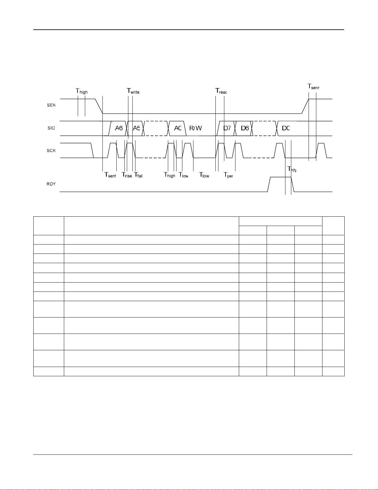
Figure 1 and Table 2 shows the timing specification
for the 3-wire serial programming interface.
Figure 1. Programming Interface Timing.
Symbol Parameter
Min. Typ. Max.
Values
Units
Tper Min. period of SCK 50 ns
Thigh Min. high time of SCK 20 ns
Tlow Min. low time of SCK 20 ns
Tfall Max. time of falling edge of SCK 1
Trise Max. time of rising edge of SCK 1
Tsenf Min. time of falling edge of SEN to falling edge of SCK 0 ns
Tsenr Min. delay from rising edge of SEN to rising edge of SCK 5 ns
Twrite
Tread
Trdy
Thigh
Time from power up to first falling edge of SEN
Min. delay from valid SIO to falling edge of SCK during a
write operation
Min. delay from rising edge of SCK to valid SIO during a read
operation (assuming load capacitance of SIO is 25pF)
Min. delay from falling edge of SCK (last bit of byte into data
buffer) to falling edge of RDY
Min. duration of a SEN high pulse
(Fphd is the phase detector frequency)
Table 2. Timing Specification for the 3-wire Programming Interface.
0 ns
75 ns
20 ns
1/Fphd
3.5 ms
µs
µs
April 2006
8
M9999-041906
(408) 955-1690
Page 9
Micrel MICRF405
Writing to the Control Registers in MICRF405
Writing: A number of octets are entered into
MICRF405 followed by a load-signal to activate the
new setting. Making these events is referred to as a
“write sequence.” It is possible to update all, 1, or n
control registers in a write sequence. The address to
write to (or the first address to write to) can be any
valid address (0-29). The SIO line is always an input
What to write:
• The address of the control register to write to (or
if more than 1 control register should be written
to, the address of the 1st control register to write
to).
• A bit to enable reading or writing of the control
registers. This bit is called the R/W bit.
• The values to write into the control register(s).
to the MICRF405 (output from user) when writing.
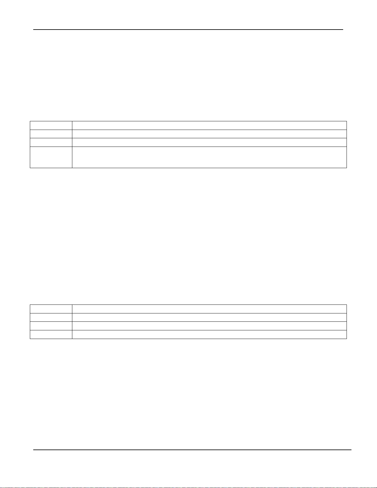
Field Comments
Address: A 7-bit field, ranging from 0 to 29. MSB is written first.
R/W bit: A 1-bit field, = “0” for writing
Values: A number of octets (1-30 octets). MSB in every octet is written first. The first octet is written to the control
register with the specified address (=”Address”). The next octet (if there is one) is written to the control
register with address = “Address + 1” and so on.
Table 3. Writing to the Control Registers.
How to write:
Bring SEN low to start a write sequence. The active
state of the SEN line is “low”. Use the SCK/SIO
serial interface to clock in “Address” and “R/W” bit
and “Values” into the MICRF405. MICRF405 will
sample the SIO line at negative edges of SCK. Make
sure to change the state of the SIO line before the
negative edge, for instance on positive edge. Refer
to Figure 2.
Bring SEN inactive to make an internal load-signal
and complete the write-sequence. Note: there is an
exception to this point. If the programming bit called
“load_en” (D0 in ControlRegister0) is “0”, then no
load pulse is generated.
Field Comments
Address: 7 bit = A6, A5, …A0 (A6 = MSB. A0 = LSB)
R/W bit: “0” for writing
Values: 8 bits = D7, D6, …D0 (D7 = MSB, D0 = LSB)
Table 4. When writing to a Single Register, totally 2 octets are clocked into the MICRF405.
How to write:
• Bring SEN low
• Use SCK and SIO to clock in the 2 octets
• Bring SEN high
The two different ways to “program the chip”
are:
• Write to a number of control registers (0-29)
when the registers have incremental addresses
(write to 1, all or n registers)
• Write to a number of control registers when the
registers have non-incremental addresses.
Writing to a Single Register
Writing to a control register with address “A6, A5,
…A0” is described here. During operation, writing to
1 register is sufficient to change the way the
transmitter works. Typical example: Change from
transmit mode to power-down.
April 2006
9
M9999-041906
(408) 955-1690
Page 10
Micrel MICRF405
Internal load pulse
generated here
SEN
Register address
Data to write
into register
SIO
SCK
A6A5A4 A3 A2
A1 A0
Figure 2. Writing to One Address.
In Figure 2, SIO is changed at positive edges of
SCK. The MICRF405 samples the SIO line at
negative edges. The value of the R/W bits is always
“0” for writing.
Writing to All Registers
Writing to all register can be done at any time. To
get the simplest firmware, always write to all
registers. The price to pay for the simplicity is
increased write-time, which leads to increased time
to change the way the MICRF405 works. If data is
transferred through DATAIN pin write address 0-23
(address 24-29 is don’t care). If data is transferred
through SPI write address 0-28 (Address 29 is only
written to during data transfer, not during
configuration).
R/W
D7 D6
D5 D4 D3
D2 D1
D0
What to write
Field Comments
Address: ‘0000000’ (address of the first register to write to, which is 0)
R/W bit: “0” for writing
Values: 1st Octet: wanted values for ControlRegister0. 2nd Octet: wanted values for ControlRegister1 and
so on for all of the octets.
Table 5. When writing to All Registers, totally 25/30 (5 are optional) octets are clocked into the MICRF405.
How to write:
• Bring SEN low
• Use SCK and SIO to clock in the 25/30 octets
• Bring SEN high
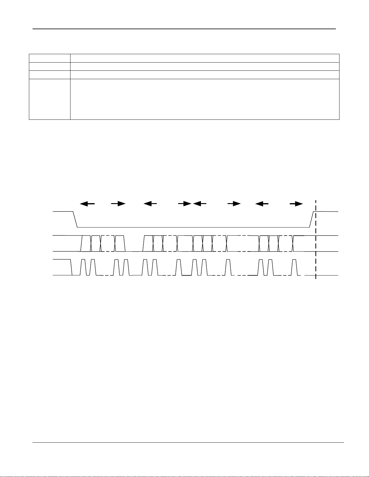
Refer to Figure 3. Writing to n Registers Having
Incremental Addresses.
April 2006
Writing to n Registers Having Incremental
Addresses
In addition to entering all bytes, it is also possible to
enter a set of n bytes, starting from address i = “A6,
A5, … A0”. Typical example: Clock in a new set of
frequency dividers (i.e. change the RF frequency).
Registers to be written are located in i, i+1, i+2.
10
M9999-041906
(408) 955-1690
Page 11
Micrel MICRF405
What to write
Field Comments
Address: 7 bit = A6, A5, …A0 (A6 = MSB. A0 = LSB) (address of first byte to write to)
R/W bit: “0” for writing
Values: n* 8 bits =
D7, D6, …D0 (D7 = MSB, D0 = LSB) (written to control reg. with address ”i”)
D7, D6, …D0 (D7 = MSB, D0 = LSB) (written to control reg. with address ”i+1”)
D7, D6, …D0 (D7 = MSB, D0 = LSB) (written to control reg. with address ”I+n-1”)
Table 6. When writing to Registers having Incremental Addresses, totally 1+n octets are clocked into the MICRF405.
How to write:
• Bring SEN low
• Use SCK and SIO to clock in the 1 + n octets
• Bring SEN high
Internal load pulse
generated here
SEN
Register i
address
Data to write
into register
i
Data to write
into register
i +1
Data to write
into register
i + n - 1
SIO
SCK
A5 A0
A6
R/W
D7 D6
D0
D7 D6
D0
D7 D6 D0
Figure 3. Writing to n Registers Having Incremental Addresses.
April 2006
11
M9999-041906
(408) 955-1690
Page 12
Micrel MICRF405
Writing to n Registers having Non-Incremental
Addresses
Registers with non-incremental addresses can be
SEN
Register addr ess
Data read
from register
Internal load pulse
generated here
written to in one write-sequence as well. Example of
non-incremental addresses: “0,1,3”. However, this
SIO
A6A5A4 A3A2
A1 A0
R/W
D7 D6
D5 D4 D3
D2 D1
D0
requires more overhead, and the user should
consider the possibility to make a “continuous”
update, for example, by writing to “0,1,2,3” (writing
the present value of “2” into “2”). The simplest
firmware is achieved by always writing to all
SCK
SIO INPUT
SIO OUTPUT
SAMPLE TIME
registers. Refer to previous sections.
This write-sequence is divided into several subparts:
• Disable the generation of load-signals by
clearing bit “load_en” (D0 in ControlRegister0)
• Repeat for each group of register having
incremental addresses:
- Bring SEN active
- Enter first address for this group, R/W bit and
values
- Bring SEN inactive
• Finally, enable and make a load-signal by
setting “load_en”
Refer to the previous sections for how to write to 1 or
n (with incremental addresses) registers in the
MICRF405.
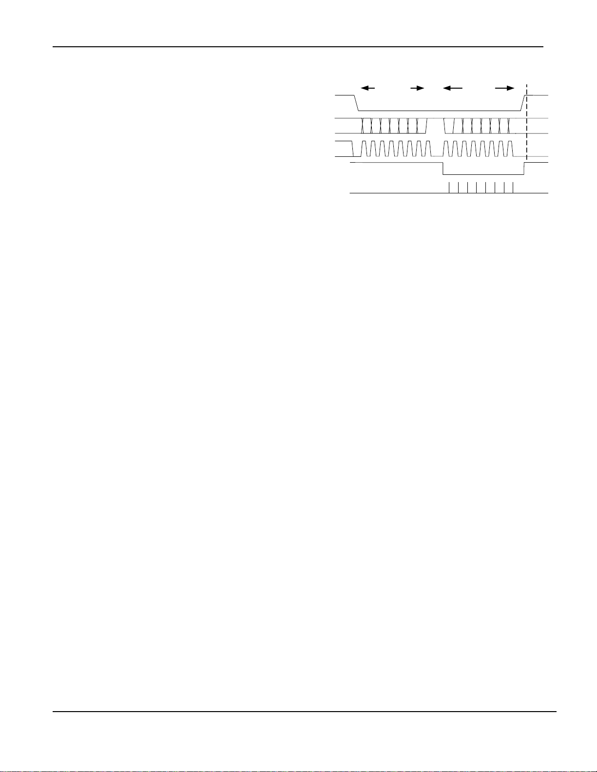
Reading from the Control Registers in MICRF405
The “read-sequence” is:
1. Enter address and R/W bit
2. Change direction of SIO line
3. Read out a number of octets and change SIO
direction back again.
It is possible to read all, 1 or n registers. The
address to read from (or the first address to read
from) can be any valid address (0-29). Reading is
not destructive, i.e., values are not changed. The
SIO line is output from the MICRF405 (input to user)
for a part of the read-sequence. Refer to procedure
description below.
A read-sequence is described for reading n
registers, where n is number 1-30.
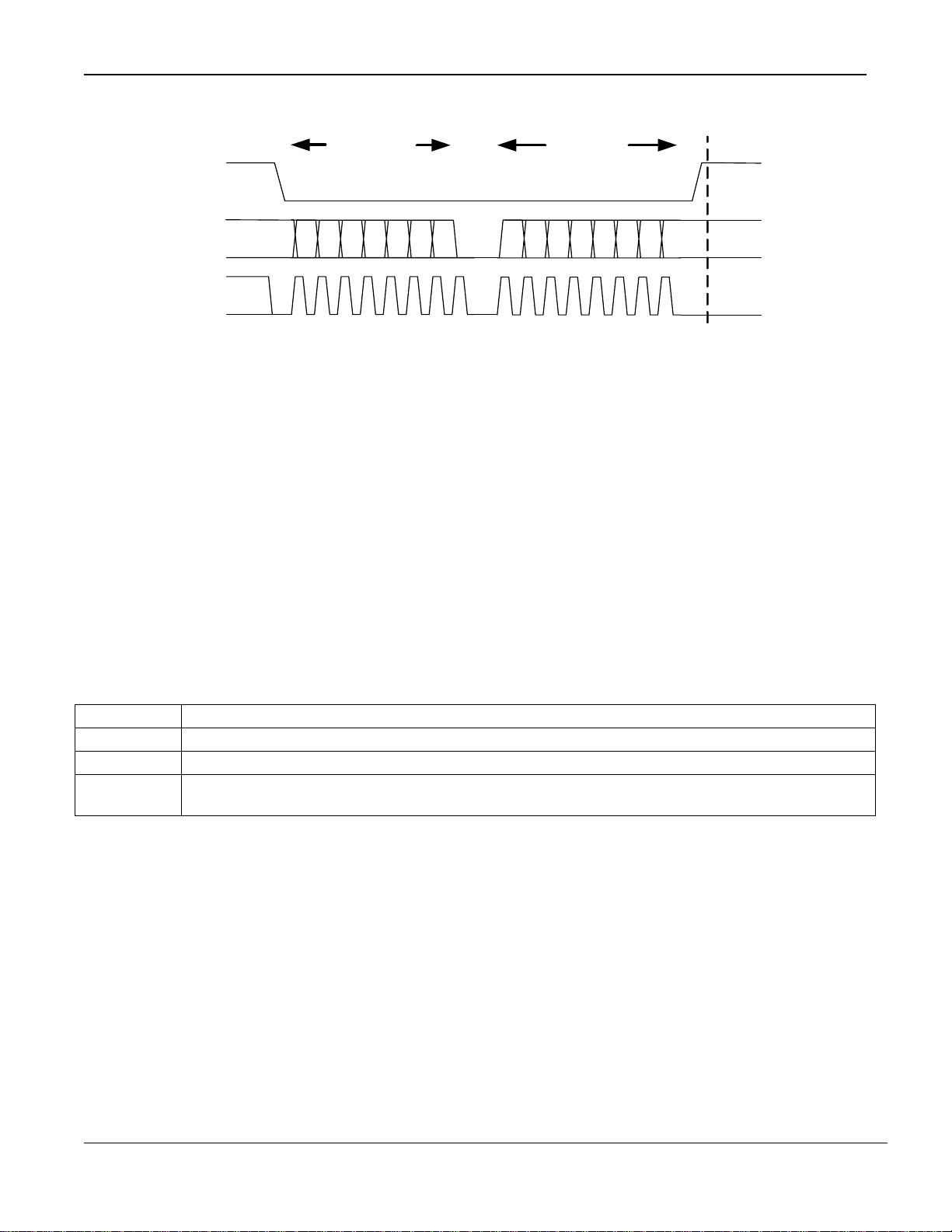
Figure 4. Reading from a Control Register.
In Figure 4 above, 1 register is read. The address is
A6, A5, … A0. A6 = MSB. The data read out is D7,
D6, …D0. The value of the R/W bit is always “1” for
reading.
• Bring SEN low
• Enter address to read from (or the first address
to read from) (7 bits) and
• The R/W bit = 1 to enable reading
• Make the SIO line an input to the user (set pin in
tristate)
• Read n octets. The first rising edge of SLK will
set the SIO as an output from the MICRF405.
The 405 will change the SIO line at positive
edges of SCK. The user should read the SIO
line at the negative edges.
• Make the SIO line an output from the user again.
Reading from the Interrupt Register
If any of the interrupts, Vc_HI, Vc_LO or Low_Batt,
is set the SRV pin will go high. Read the interrupt
register, address 24, to see which interrupts are
flagged. It is possible to read this register at all
times, for instance, to read the tuned VCO_FREQ
setting which is also stored at the same address.
When rising SEN after haveing read the register, the
internal load pulse will then clear all interrupt flags.
To keep the flags when reading it, it is therefore
necessary to set LOAD_en=0 before hand.
April 2006
12
M9999-041906
(408) 955-1690
Page 13
Micrel MICRF405
Data Interface and Data Transfer
Adr Data
A6..A0 D7 D6 D5 D4 D3 D2 D1 D0
0000000 Mode1=0 Mode0=1 PA2=1 PA1=1 PA0=1 ClkOut_en=1 Sync_en=1 Load_en=1
0001100 LowBatt_level=0 LDO_by=0 LDO_en1=1 LDO_en0=1 MOD_LDc_en=0 PA_FEc_en=0 PA_LDc_en= 0 LD_en=1
0001101 Bit_IO_en=1 Manchester_en=0 Sel_CRC1=1 Sel_CRC0=1 SyncID_Len1=0 SyncID_Len0=1 Pream_Len1=1 Pream_Len0=0
0011001 SyncID3_7=1 SyncID3_6=1 SyncID3_5=1 SyncID3_4= 0 SyncID3_3= 0 SyncID3_2=1 SyncID3_1=0 SyncID3_0=1
0011010 SyncID2_7=1 SyncID2_6=1 SyncID2_5=1 SyncID2_4= 0 SyncID2_3= 0 SyncID2_2=1 SyncID2_1=0 SyncID2_0=1
0011011 SyncID1_7=1 SyncID1_6=1 SyncID1_5=1 SyncID1_4= 0 SyncID1_3= 0 SyncID1_2=1 SyncID1_1=0 SyncID1_0=1
0011100 SyncID0_7=1 SyncID0_6=1 SyncID0_5=1 SyncID0_4= 0 SyncID0_3= 0 SyncID0_2=1 SyncID0_1=0 SyncID0_0=1
0011101 DATA_7 DATA_6 DATA_5 DATA_4 DATA_3 DATA_2 DATA_1 DATA_0
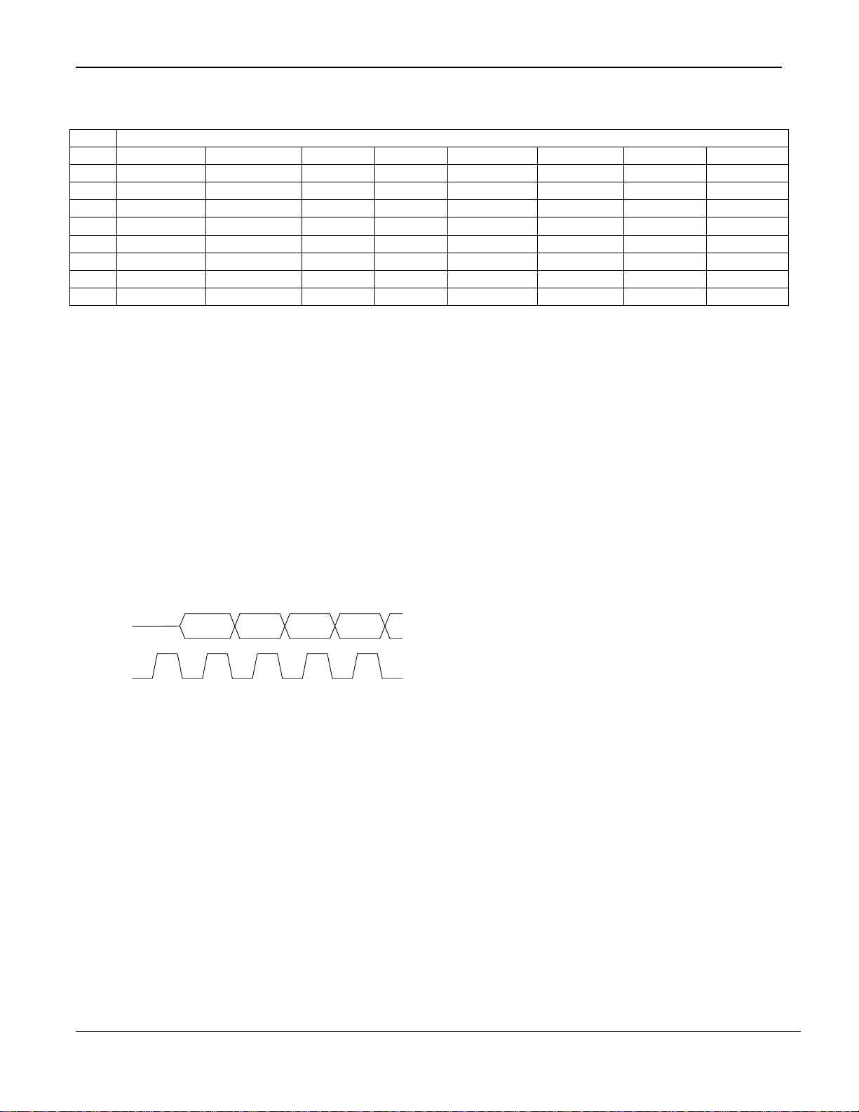
There are two main data interfaces; bit-wise and
byte oriented. The bit-wise interface use the DATAIN
(always input to the 405) and DATACLK pin (always
output from the 405). This interface is enabled with
the Bit_IO_en=”1”. If Sync_en=1 bit-wise
synchronous mode is selected and data clock is
provided on the RDY/DATACLK pin. In this mode,
the MICRF405 will sample the bit on the DATAIN pin
on the positive edge of the DATACLK. It is therefore
important that the MCU toggle the DATAIN pin on
negative edge of the DATACLK, See Figure 5. No
packet engine, CRC or Manchester encoding is
available in bit-wise data interface. To select
asynchronous mode set Sync_en=”0”. If VCO
modulation is selected, the DATAIN pin in tri-state
(MCU pin=input) until first bit is about to be
transmitted (see VCO modulation).
DATAIN
DATACLK
Figure 5. Synchronous Data Interface.
If Bit_IO_en=0, the byte wise interface is selected
and data is transferred byte wise through the one
byte buffer (register address 29). The register is
accessed the same way as the other register, as
explained in the previous sections. The only
difference is that it is instantly valid and do not need
any load pulse. This also applies to the SyncID
registers, address 25-28. When writing to address
29, the address counter will not increment which
means several bytes can be written into the buffer
without raising SEN and setting up a new write
session. The RDY/DATACLK pin will provide byte
synchronization. The data byte buffer is ready for
refill on falling edges on RDY. In this mode of data
transfer, Sync_en must be set.
The data in the buffer is fed into a packet engine
with an optional CRC calculation and Manchester
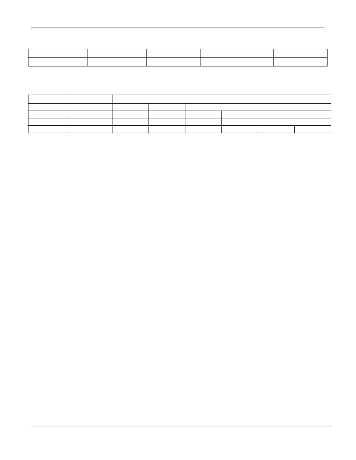
encoding. The virtual wire packet structure is shown
in Table 7. The preamble, SyncID field and CRC
field are automatically generated by the packet
engine. The user needs only to enter frame length
and payload for each packet. The preamble bytes
are equal to 10101010, and the number of preamble
bytes are given by 1+Pream_Len[1:0] (D1:D0
ControlRegister13). Next field is the SyncID which is
1-4 bytes long set by the SyncID_Len[1:0] bits. The
content of the SyncID bytes are fully programmable
and specified in the SyncID0-3 bytes. The SyncID0
byte, address 28, is sent first, and the SyncID3 byte,
address 25, is sent last. Refer to Table 8. The frame
length byte follows the SyncID field. It specifies
length of the payload and CRC. Finally, the CRC
field ends the packet. The SelCRC_0 bit specifies
the length of the CRC field. If it is set, a 2 byte ITU-T
CRC (start condition 00h) is calculated of the
payload and sent. If SelCRC_0=0, an 8 bit CCITT
CRC is calculated of the payload and sent. Either
two cases assuming SelCRC_1=1. If SelCRC_1=0,
no CRC is calculated on chip, and the user must
calculate this on the microcontroller and include it in
the payload. A Manchester encoder is available on
chip. It is activated if the Manchester_en bit is set. It
encodes the complete packet. The codes are “10”
for “0” and “01” for “1”. The preamble byte is
automatically set 0 in this mode, as this will produce
the desired 10101010-pattern when Manchester
encoded. Note that on-the-air data rate will be twice
the bit rate set by the FSKClk_K/FSKn or
ASKClk_K/ASKn, which specifies the actual
throughput. Because of this, FSKn needs to be
greater than zero if VCO modulation is selected,
Modulation[1:0]<2.
April 2006
13
M9999-041906
(408) 955-1690
Page 14
Micrel MICRF405
Preamble SyncID Frame length Payload CRC
1-4 bytes 1-4 bytes 1 byte 2/2/1-253/254/255 bytes 2/1/0 bytes
Table 7. Virtual Wire Packet Structure Overview.
SyncID_Len SynchID_Len Start of transmitted packet. Leftmost byte transmitted first
0 0 Preamble SyncIDO Frame length
0 1 Preamble SyncIDO SyncID1 Frame length
1 0 Preamble SyncIDO SyncID1 SyncID2 Frame length
1 1 Preamble SyncIDO SyncID1 SyncID2 SyncID3 Frame length
Table 8. Virtual Wire Packet Structure, SyncID field.
Packet Engine Overview:
• Preamble generated by packet engine: 1-4 bytes equal 10101010. Length set by Pream_Len[1:0]
• SyncID field added by packet engine: 1-4 bytes of user defined content. Length set by SyncID_Len[1:0].
Content set in registers SyncID0, SyncID1, SyncID2 and SyncID3, address 28-25.
• The frame length is entered by user for each packet. Specify the length of the payload and CRC fields in
bytes, ranging from 2 to (255 ÷ # CRC bytes). # CRC bytes can be 0 to 2.
• For each payload byte, wait for falling edge of RDY before writing the byte into the DATA register.
• The optional CRC field ends the packet. Its length is programmable 0, 1 or 2 bytes by the Sel_CRC[1:0].
April 2006
14
M9999-041906
(408) 955-1690
Page 15
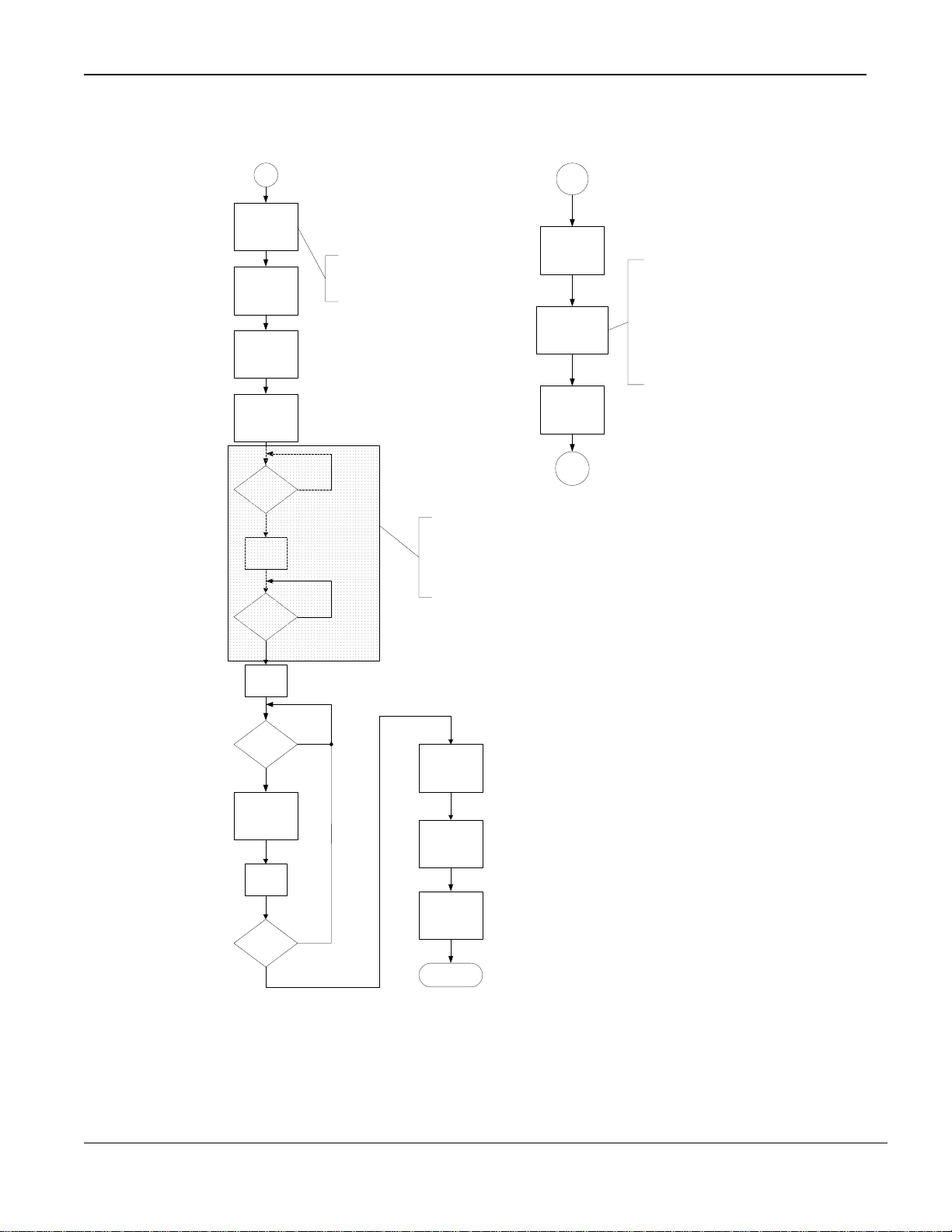
Micrel MICRF405
How to transmit a Packet with the Packet Engine:
Send
data
CALL PROG
[TX]
INIT WRITE
SEQUENCE
[SET SEN=”0"]
INIT TX BUFFER
[WRITE ADDR 2 9,
R/W =”0"]
WRITE FRAME
LENGTH
PLL IN LOCK?
PLL IN LOCK?
NO
[LD=”1"]
YES
TURN on
PA
[LD=”1"]
YES
MICRF405 INTERNAL PROCESS
i=0
stable the MICRF405
NO
MICRF405 starts the
XCO. When XCO is
powers up the LDOs
and starts the PLL.
MICRF405 waits for
the PLL to lock;
LD=”1", Turns on PA
and waits for the PLL
to lock with PA on;
”LD=1", the n start to
send Preamble,
SyncID and Frame
length.
PROG
INIT WRITE
SEQUENCE
[SET SEN=”0"]
WRITE CONTROL
WORD
[ADDRESS + R/W +
CONTROL WORD]
LOAD CONTROL
WORD
[SET SEN=”1"]
RETURN
Control word, e.g:
TX mode:
Mode1-0=3 [TX]
PA_LDc=”1"[Turns on PA
stage when PLL is in lock]
MOD_LDc_en=”1"
[Modulation starts once
frame length is written into
data byte and PA is turned
on and LD is high.]
PA_FEc_en=”1" [The PA is
turned off immediately after
last bit in packet is sent.]
Power down mode:
Mode1-0=0
April 2006
edge?
BYTE i
i=1+1
i=n?
YES
YES
NO
NO
Wait for [2 +
number of CRC
bytes] falling edge
of RDY. Then wait
1 bit periode.
END TX msg
sequence
[SEN=”1"]
CALL PROG
[Power down]
END
RDY = falling
WRITE PAYLOAD
Figure 6. Flowchart of Transmitting a Packet Using the Packet Engine.
15
M9999-041906
(408) 955-1690
Page 16

Micrel MICRF405
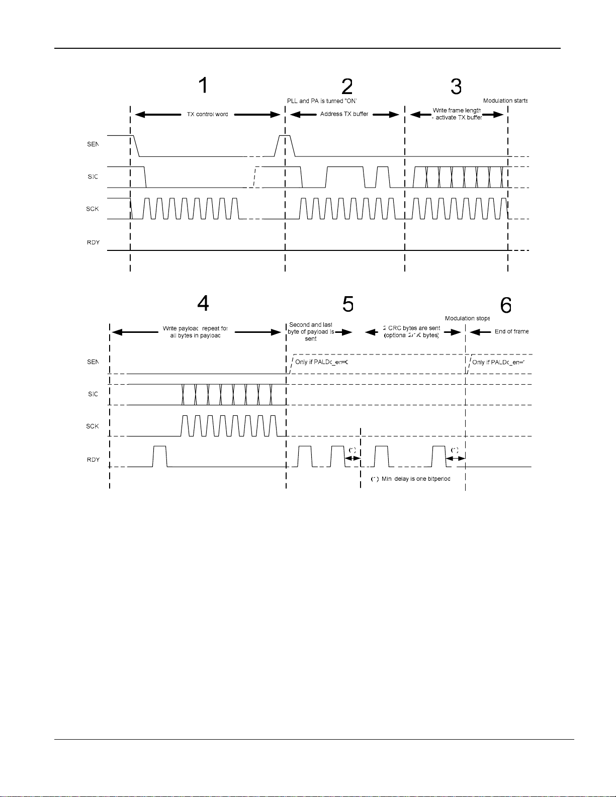
The sequence of a typically packet transfer is shown
in Figure 7.
1. Set the 405 in transmit mode with the correct
settings by writing in the TX control word.
Once SEN is pulled high, the internal load will
activate the new settings. The 405 will now
start the PLL and turn on the PA (if
PA_LDc_en is set)
2. Pull SEN low, and address the TX buffer.
Address=29+R/W, RW=”0”.
3. Write the frame length into the data buffer. On
th
the 8
falling edge of SCK, clocking in the last
bit, the modulation will start. If MOD_LDc_en is
not set, check that lock detect (LD) is high after
PA is turned on before writing last bit (or the
complete byte 3). If MOD_LDc_en=1, finish
steps 2 and 3 immediately after step 1. The
MICRF405 will now wait until the transmitter is
ready (PLL tuned in, PA on and LD high)
before starting to modulate. In either case, the
packet engine will start to transmit the desired
preamble and SyncID bytes once the
modulation starts.
4. When the last bit of the last SyncID byte is
being sent, the RDY signal is high. After the
falling edge of RDY, the packet engine is
sending the frame length, and the buffer is
then ready for refill. The time between 3 and 4
will vary depending, upon the bit rate and
desired number of bytes in the preamble and
SyncID field. The first RDY pulse will, however,
notify the user when to enter the 1
st
byte of the
payload. Step four is repeated for all the bytes
in the payload, meaning [frame length –
number of CRC bytes] times. It is important
that the buffer is refilled after the falling edge of
RDY and before the next falling edge of RDY.
means that the SEN now can be pulled high at
any time, closing the write session. If
PA_LDc_en=1 and load_en=1, it is then
necessary to leave SEN low until the end of
packet. This is because raising SEN will
generate a load pulse, and this, in turn, causes
the PA_LDc function to turn off the PA for a
short period of time. The RDY signal will be
high when the last bit of the payload is being
sent, but there is now no need to refill the
buffer. Also, if CRC is enabled, then RDY will
be high during the last bit of each of the CRC
bytes being sent. Because of an internal
sampling the actual RF output lags 1 bit
period, which means the modulation will stop
one bit period after the last RDY pulse.
6. The frame is now completely transmitted. If
PA_FEc_en=1, the PA will be automatically
turned off immediately after last bit in packet is
transmitted. The PLL will, however, remain
running. (This state is equal to MODE[1:0]=3
(TX), PA_LDc_en=0 and PA[2:0]=0.) If
PA_FEc_en=0 the PA will remain on until it is
turned off by the MODE or PA bits. In step 6,
the buffer is ready for a new packet. Any 8bits
entered into the buffer in this sections is
though of as a new frame length, refer back to
Section 3. This, assuming the MICRF405
remains in TX (MODE[1:0]=3). In this case,
and when PA_FEc_en=1, the PA will be turned
on once the 8
th
bit is clocked in. It is
recommended to use the MOD_LDc function in
this case as it will delay the modulation until
the PLL has stabilized after the PA is turned
on. If not the start of the modulation will be
distorted and may interfere the settling of the
PLL due to PA turn on (please see chapter
Lock Detect).
5. In this step, all user data is received in the 405
and it transmits the last part of the packet. This
April 2006
16
M9999-041906
(408) 955-1690
Page 17
Micrel MICRF405
Figure 7. Sequence of a Typical Packet Transfer.
Programming Summary
• Use SEN, SCK, and SIO to get access to the
control registers in MICRF405.
• SCK is user-controlled.
• Write to the MICRF405 on positive edges
(MICRF405 reads on negative edges).
• Read from the MICRF405 on negative edges
(MICRF405 writes on positive edges)
• Address field is 7 bits long. Enter MSB first.
• R/W bit is “1” for read and “0” for write.
• Address and R/W bit together make 1 octet
• Enter/read MSB in every octet first.
April 2006
• Always write 8 bits to/read 8 bits from a control
register. This is the case for registers with less
than 8 used bits as well.
• Writing: Bring SEN low, write address and R/W
bit followed by the new values to fill into the
addressed control register(s) and bring SEN
high for loading, i.e. activation of the new control
register values (“Load_en” = 1).
17
M9999-041906
(408) 955-1690
Page 18
Micrel MICRF405
Main Modes of Operation
Adr Data
A6..A0 D7 D6 D5 D4 D3 D2 D1 D0
0000000 Mode1=0 Mode0=1 PA2=1 PA1=1 PA0=1 ClkOut_en=1 Sync_en=1 Load_en=1
There are three main modes of operation and these
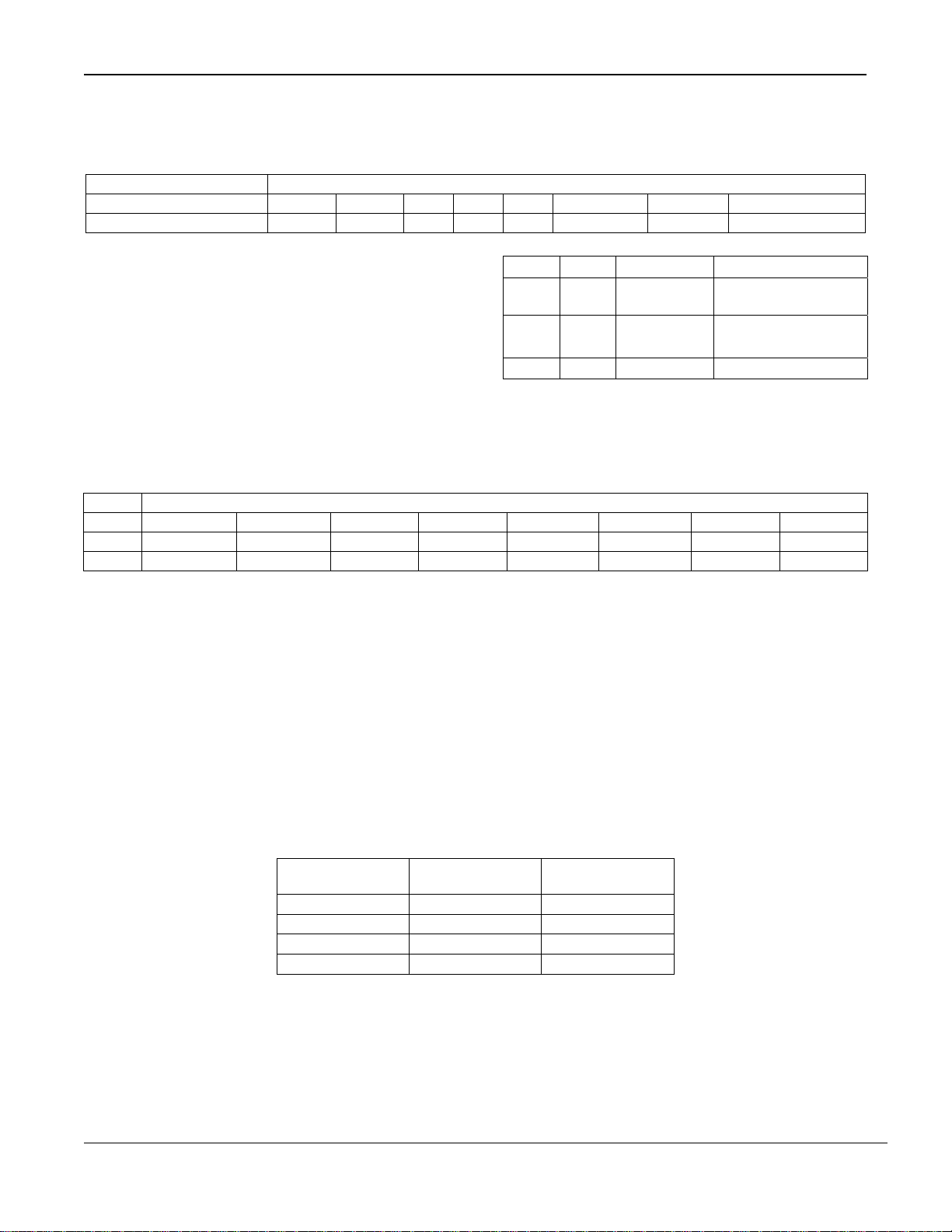
are controlled by Mode1-0, see Table 9. In “Power
down” mode all blocks are shut down, though the
contents of the registers are preserved. In “Standby”
the crystal oscillator is running and an optional
programmable clock is present on the CLKOUT pin
(Default enabled). This clock can be used as a
micro-controller reference frequency. In “TX“ mode
all blocks are active if not disabled by the user.
Mode1 Mode0 State Comments
0 0 Power down
0
1
1 1 Transmit mode Transmit mode
1
0
Table 9. MICRF405 Main Modes.
Standby
Keeps Register
configuration
Crystal Oscillator
running
Power Amplifier
Adr Data
A6..A0 D7 D6 D5 D4 D3 D2 D1 D0
0000000 Mode1=0 Mode0=1 PA2=1 PA1=1 PA0=1 ClkOut_en=1 Sync_en=1 Load_en=1
0010111 PA_IB3=1 PA_IB2 =0 PA_IB1=0 PA_IB0=1 PAB_IB3=1 PAB_IB2=0 PAB_IB1=0 PAB_IB0=1
The maximum output power is approximately
10dBm. For maximum output power the load seen
by the PA must be resistive and around 150Ω at
900MHz and 250Ω at 434MHz and 315Hz. The
output power can be programmed with bits PA[2:0]
to eight different levels if bit PA_LDc_en=1 or seven
levels if PA_LDc_en=0, with approximately 3dB
between each step. If PA_LDc_en=0, the PA is
turned of by setting PA[2:0] to 0. For all other
PA[2:0] combinations, the PA is on and has a
maximum power when PA[2:0]=7. If PA_LDc_en=1
the PA is controlled by the lock detector.
A simple π LC network can be used to provide the
Frequency band
(MHz)
315 8 8
434 9 8
868 9 9
915 10 9
Table 10. Recommended Settings of PA_IB and PAB_IB vs. Frequency Band.
PA_IB[2:0] PAB_IB[2:0]
needed impedance and also to reduce the power of
the harmonics to acceptable levels. Such matching
networks for different frequencies are shown on the
Typical Application Circuit.
The bias setting of the PA and the PA buffer is
controlled by bits PA_IB PA[2:0] and PAB_IB
PA[2:0]. The recommended bit setting, shown in
Table 10, is for the different frequency bands.
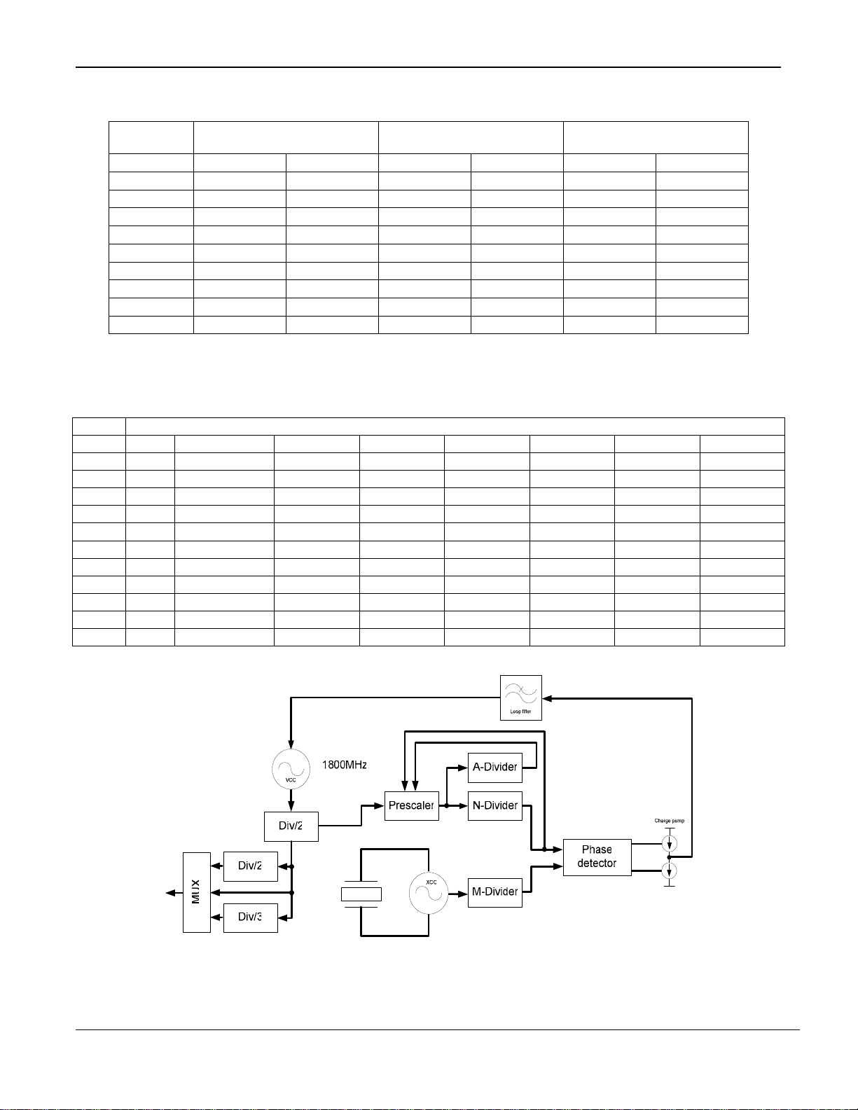
Typical values of output power and current
consumption for the different power levels for
different frequencies are shown in Table 11. The
settings used are: Modulation[2:0]=2, ClkOut_en=0,
external loop filter.
April 2006
18
M9999-041906
(408) 955-1690
Page 19
Micrel MICRF405
Power level
(PAx)
P
out
7 10.0 17.5 10.3 16.8 10.5 16.4
6 5.8 13.2 7.0 13.0 8.6 13.3
5 3.1 11.5 4.3 11.6 5.7 11.5
4 0.5 10.5 1.7 10.6 2.8 10.2
3 -1.9 9.9 -1.1 10.0 -0.1 9.3
2 -4.2 9.5 -3.8 9.5 -3.2 8.6
1 -6.7 9.1 -6.8 9.2 -6.5 8.2
0 -9.2 8.9 -9.8 9.0 -9.7 7.9
PA off 5.4 6.1 5.4
Table 11. Output Power and Current Consumption vs. Power Level Setting (PA2..PA1) for 315, 434 and 915MHz.
915MHz 434MHz 315MHz
(dBm) I
(mA) P
VDD
(dBm) I
out
(mA) P
VDD
(dBm) I
out
VDD
(mA)
Frequency Synthesizer
Adr Data
A6..A0 D7 D6 D5 D4 D3 D2 D1 D0
0000001 - - A0_5=0 A0_4=0 A0_3=1 A0_2=1 A0_1=1 A0_0=0
0000010 - - - - N0_11=0 N0_10=0 N0_9=0 N0_8=0
0000011 N0_7=0 N0_6=1 N0_5=1 N0_4=1 N0_3=0 N0_2=0 N0_1=1 N0_0=1
0000100 - - - - M0_11=0 M0_10=0 M0_9=0 M0_8=0
0000101 M0_7=0 M0_6=0 M0_5=1 M0_4=0 M0_3=0 M0_2=0 M0_1=0 M0_0=1
0000110 - - A1_5=0 A1_4=1 A1_3=1 A1_2=1 A1_1=1 A1_0=1
0000111 - - - - N1_11=0 N1_10=0 N1_9=0 N1_8=0
0001000 N1_7=0 N1_6=1 N1_5=1 N1_4=0 N1_3=1 N1_2=1 N1_1=1 N1_0=1
0001001 - - - - M1_11=0 M1_10=0 M1_9=0 M1_8=0
0001010 M1_7=0 M1_6=0 M1_5=1 M1_4=0 M1_3=0 M1_2=0 M1_1=0 M1_0=0
0010000 ‘0’ Prescaler_Sel=0 FSKClk_K5=1 FSKClk_K4=1 FSKClk_K3=0 FSKClk_K2=1 FSKClk_K1=0 FSKClk_K0=0
April 2006
Figure 8. PLL Block Diagram.
19
M9999-041906
(408) 955-1690
Page 20

Micrel MICRF405
The frequency synthesizer consists of a voltagecontrolled oscillator (VCO), crystal oscillator,
prescaler, programmable frequency dividers, phasedetector and charge pumps. Two different types of
prescalers are integrated, a pulse swallow and a
phase select prescaler. The recommended prescaler
is the phase select prescaler (Prescaler_Sel=0,
which is default). There is both a configurable onchip loop filter and an external loop filter. The
lengths of the N and M and A registers are 12, 12
and 6 bits respectively. The M, N and A values can
be calculated from the formula:
Phase select prescaler (Prescaler_Sel=0):
f
f
XCO
=
RF
kM
⋅
)31( AN
+
Pulse swallow prescaler (Prescaler_Sel=1):
f
f
XCO
= ,
RF
kM
⋅
)232( AN
+
where:
f
: Crystal oscillator frequency
XCO
f
: RF frequency
RF
0 < A
≤ N
k: 6: RF frequency 290-325 MHz,
Freq_Band[1:0]=0
4: RF frequency 430-490 MHz,
Freq_Band[1:0]=1
2: RF frequency 860-980 MHz,
Freq_Band[1:0]=2-3
There are two sets of each of the divide factors (i.e.
A0 and A1). If modulation by using the dividers is
selected Modulation1=1, Modulation0=0), the two
sets should be programmed to give two RF
frequencies, separated by two times the specified
single sided frequency deviation. For all other
modulation methods, the 0-set will be used. The
value of A is constrained to be less or equal to N,
0<=A<=N.
April 2006
20
M9999-041906
(408) 955-1690
Page 21
Micrel MICRF405
Crystal Oscillator (XCO)
Adr Data
A6..A0 D7 D6 D5 D4 D3 D2 D1 D0
0010101 ClkOut_1=0 ClkOut_0=0 XCO_Fast=1 XCOtune4=1 XCOtune3=0 XCOtune2=0 XCOtune1=0 XCOtune0=0
The crystal oscillator is a very critical block. As the
crystal oscillator is a reference for the RF output
frequency, very good phase and frequency stability
is required. When selecting crystal it should be paid
special attention to the total frequency tolerance and
load capacitance as these will directly influence on
the carrier frequency.
XTB, pin 7 XTA, pin 8
C2C1
Figure 9. Crystal Oscillator Circuit.
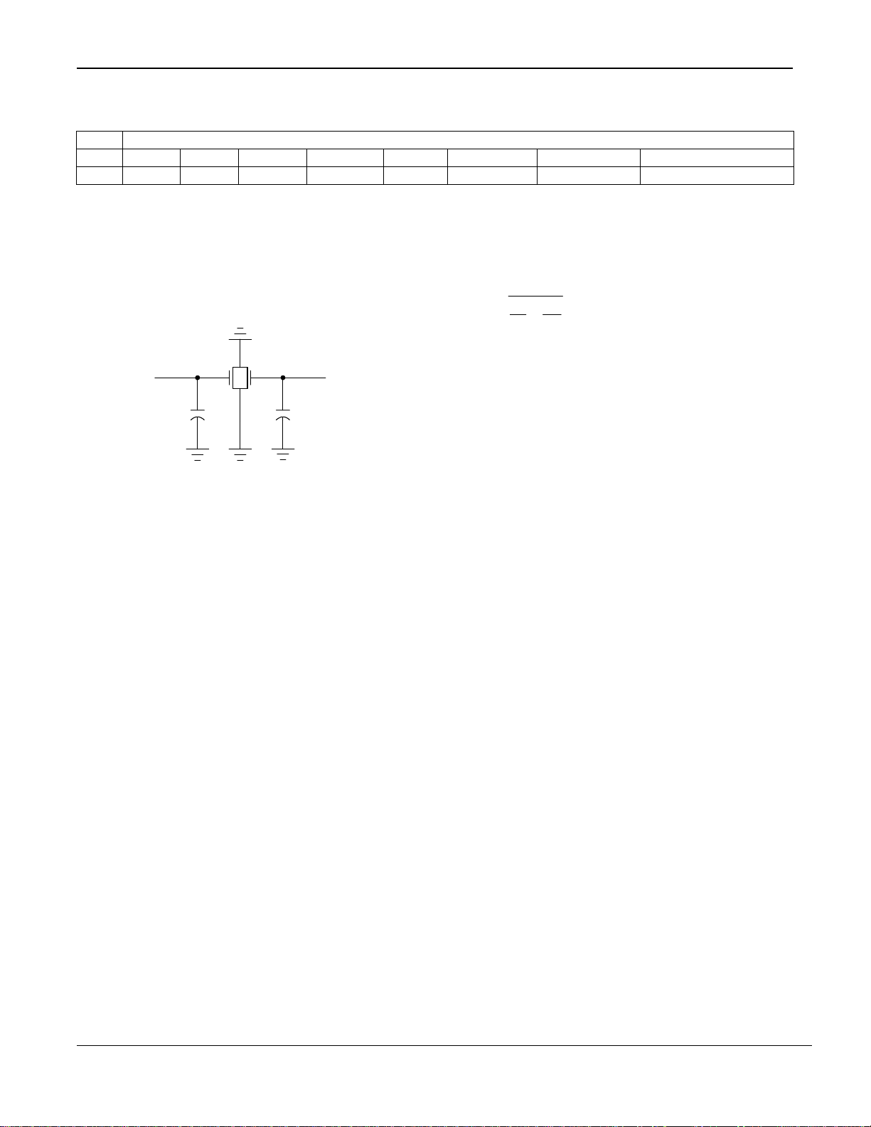
The crystal should be connected between pins XTA
and XTB (pin 7 and 8). MICRF405 has an internal
crystal capacitor bank used for crystal tolerance
tuning during production. These internal capacitors
can be enabled using the XCOtune[4:0] bits. If
XCOtune[4:0]=0 then no internal capacitors are
connected to the crystal pins, while 18pF are
connected to each pin if XCOtune[4:0]=31. The unit
capacitance is about 0.6pF. The internal XCOtune
feature is optimized for a crystal with a load
capacitance of 9pF and will give the expected
oscillation frequency when no external capacitors
are connected and XCOtune[4:0]=16. If a crystal
requires higher load capacitance, additional
capacitors must be added off-chip (C1 and C2 in
Figure 9).
If XCOtune[4:0]=0, the loading capacitors can be
calculated by the following formula;
C +
1
=
11
+
CC
21
C
parasiticL
The parasitic capacitance is the pin input
capacitance and PCB stray capacitance. Typically
the total parasitic capacitance is around 6pF. For
instance, for a 9pF load crystal the recommended
values of the external load capacitors are 5.6pF.
The start-up time of a crystal oscillator is typically
around a millisecond. Therefore, to save current
consumption, the XCO is turned on before any other
circuit block. During start-up the XCO amplitude will
eventually reach a sufficient level to trigger the Mcounter. After counting 2 M-counter output pulses
the rest of the circuit will be turned on. The current
consumption during the prestart period is typically
205µA. If the XCO_Fast bit is set, then XCO will
start up faster, typically in about 300µs. This comes
at the expense of a higher current consumption of
typically 2mA during the period from start up until the
first output pulse of the M-divider.
If an external reference shall be used instead of a
crystal, the signal shall be applied to pin 7, XTB.
Due to internal biasing, AC coupling is
recommended for use between the external
reference and the XTB-pin.
April 2006
21
M9999-041906
(408) 955-1690
Page 22
Micrel MICRF405
VCO
Adr Data
A6..A0 D7 D6 D5 D4 D3 D2 D1 D0
0001011 LowBatt_en=1 Freq_Band1=0 Freq_B and0=1 VCO_freq2=0 VCO_freq1=1 VCO_freq0=1 Modulation1=1 Modulation0=0
0010110 INT_LF_TEST=0 VCO_IB2=0 VCO_IB1=0 VCO_IB0=0 VCO_by=0 OUTS2=0 OUTS1=0 OUTS0=0
0011000 VCO_freq_O2 VCO_freq_O1 VCO_freq_O0 VC_HI VC_LO LOW_BATT
The VCO has no external components. It oscillates
at 1.8 GHz and is divided by 2, 4 and 6 in the 900
MHz, 450 MHz or 315MHz band respectively. This
divide ratio is controlled by the Freq_Band[1:0] bits,
as shown in Table 12.
FreqBand1 FreqBand0 Comments
0 0 RF frequency 290-325 MHz
0 1 RF frequency 430-490 MHz
1 X RF frequency 860-980 MHz
Table 12. Frequency Band.
The VCO_IB setting is automatically set when
VCO_IB[2:0]=0. If VCO_IB[2:0] are programmed <>
0, it will overrule the automatic setting. Default and
recommended for automatic settings, is
VCO_IB[2:0]=0 for all frequencies.
The bias bits will optimize the phase noise, and the
frequency bits will control a capacitor bank in the
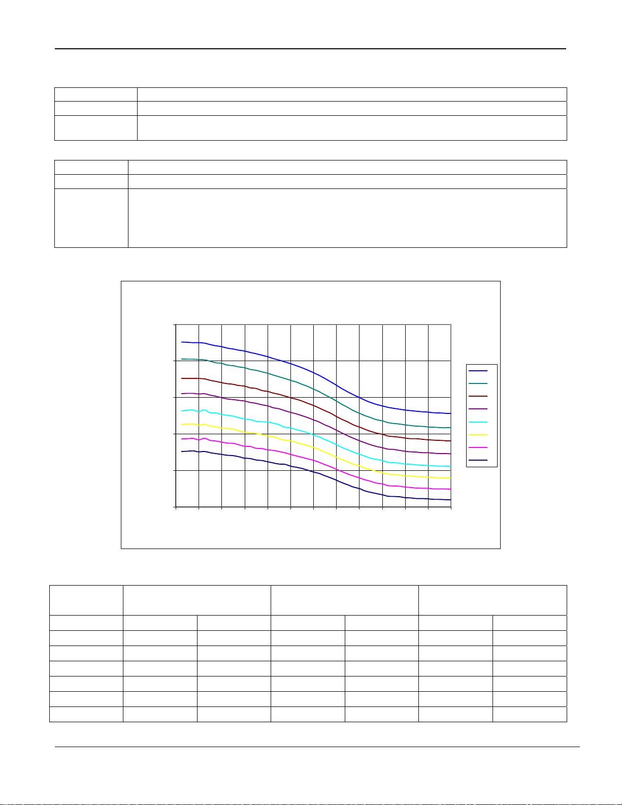
VCO. The tuning range, the RF frequency versus
varactor voltage, is dependent upon the VCO
frequency setting, and is shown in Figure 10. When
the tuning voltage is in the range from 1.2 to 1.6V,
then the VCO gain is at its maximum, approximately
60-80 MHz/V. It is recommended that the varactor
voltage is kept within this range. Table 15 shows the
recommended settings of VCO_freq and FreqBand
for various frequencies.
To ensure correct settings over variations, a circuit
monitoring the varactor voltage on start up is added.
When the PLL has locked, or after a timeout has
occurred if it doesn’t lock, this circuit will control the
varactor voltage. This will be performed if either the
VCO_Fr_Chk or VCO_Fr_Auto bit is set.
VCO_Fr_Chk set will set the interrupts VC_HI, in
case of a too high VCO_freq setting creating a too
high varactor voltage, and VC_LO, in case of a too
low VCO_freq setting creating a too low varactor
voltage. If the VCO_Fr_Auto bit is set, then the
transmitter will, if the varactor voltage is out of range,
change the programmed VCO_freq setting until the
voltage is within the range. A new setting will remain
active as long as power is on, VCO_Fr_Auto is set
and the programmed VCO_freq[2:0] bits are not
altered. The tuned VCO_freq setting of the
automatic tune circuit can be read out in the interrupt
register, VCO_Freq_O[2:0]. If both VCO_Fr_Chk
and VCO_Fr_Auto are set, each step is done by the
automatic tuning circuit that will be flagged with a
VC_LO or VC_HI interrupt. The limits of varactor
voltage used by this control circuit are between
350mV and 350mV below AVDD. The check is
performed when entering TX mode. If
PA_LDc_en=1, the control will also be executed for
each programming creating an internal load pulse
(load_en=1) while staying in TX mode. This means
that when changing frequency, the MICRF405 will
check that the VCO_Freq[2:0] settings are correct
for the new frequency. Refer to Table 13 and Table
14 for further details.
The MICRF405 must be programmed with the
recommended settings for FreqBand and VCOfreq,
as given in Table 15, even if the VCO_Fr_Chk and
VCO_Fr_Auto are enabled. This is needed to give
the VCO the correct starting values.
The VCO can be bypassed by applying a differential
local oscillator (LO) signal to the device on pin
CPOUT and VARIN. A resistor of 18k
Ω to ground
and a series capacitor of 47pF are needed on both
pins for proper biasing. The bit VCO_by must be set
to 1.
April 2006
22
M9999-041906
(408) 955-1690
Page 23
Micrel MICRF405
VCO_Fr_Chk Comments
0 VCO control voltage is not controlled
1
VCO_Fr_Auto Comments
0 No calibration is done.
1
VCO control voltage is measured; if it is below 0.35V the VC_LO interrupt flag is set, if it is higher than
AVDD-0.35V the VC_HI flag is set
Table 13. VCO Control Voltage Out of Range Detection.
If VCO control voltage is below 0.35V or above AVDD-0.35V, the VCO frequency settings are altered until
the control voltage is within the window. No VC_LO or VC_HI interrupt flag is set. The new settings can be
read out; bits VCO_Freq_O[2:0] in interrupt register.
If PLL for some reason cannot obtain lock (i.e. if frequency is set wrongly), an interrupt will be given even
if VCO_Fr_Chk = 0.
Table 14. Automatic VCO Range Calibration.
VCO Tuning Range for Var ious VCO_Freq Setti ngs
1050.0
1000.0
7
6
950.0
900.0
RF frequency [MHz]
850.0
800.0
0 0.2 0.4 0.6 0.8 1 1.2 1.4 1.6 1.8 2 2.2 2.4
Varactor Voltage [V]
5
4
3
2
1
0
Figure 10. RF Frequency vs. Varactor Voltage and VCO Frequency Bit.
VCO_freq FreqBand=0
315MHz
1 287 290 430 435 860 870
2 290 293 435 440 870 880
3 293 300 440 450 880 900
4 300 307 450 460 900 920
5 307 313 460 470 920 940
6 313 320 470 480 940 960
7 320 326 480 490 960 980
Table 15. Freq Ranges vs. VCO_freq and FreqBand.
April 2006
FreqBand=1
433MHz
23
FreqBand=2 or 3
868, 915MHz
M9999-041906
(408) 955-1690
Page 24
Micrel MICRF405
Charge Pump and PLL Filter
Adr Data
A6..A0 D7 D6 D5 D4 D3 D2 D1 D0
0010011 INT_LF_EN=1 CP_CUR1=0 CP_CUR0=1 LF_RES1_4=0 LF_RES1_3=1 LF_RES1_2=0 LF_RES1_1=0 LF_RES1_0=1
0010100 LF_High_PM=1 LF_CAP1=1 LF_CAP0=1 LF_RES3_4=0 LF_RES3_3=0 LF_RES3_2=1 LF_RES3_1=0 LF_RES3_0=1
0010110 INT_LF_TEST=0 VCO_IB2=0 VCO_IB1=0 VCO_IB0=0 VCO_by=0 OUTS2=0 OUTS1=0 OUTS0=0
There are two charge pumps, one for the external
loop filter, and one for the internal filter. Both pumps
have four different output current steps controlled by
the CP_CUR[1:0] bits (refer to Table 16). The
internal loop filter is a dual path type, which needs
two charge pump currents. The different steps allow
different bandwidths for the internal filter and give
greater flexibility when choosing components for the
external filter.
An external PLL loop filter is recommended when
using FSK modulation that is applied with dividers
and closed loop modulation using the modulator. For
Open Loop modulation a combination of external
and internal loop filter is recommended. In all modes
of ASK/OOK modulation, it is only possible to use
internal PLL loop filter due to the high bandwidth
requirements.
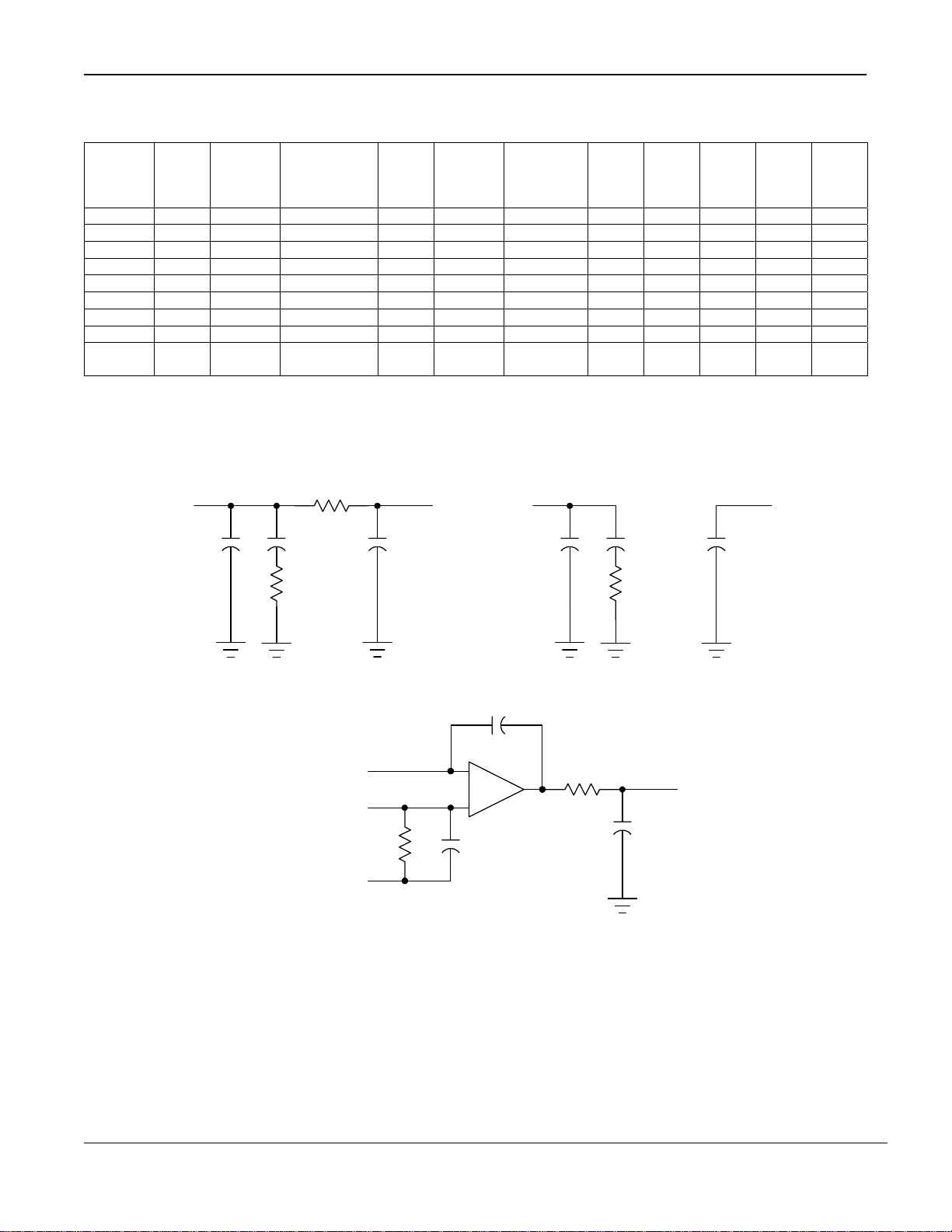
Table 15 below shows three different loop filters, the
three first are for closed loop modulation and the last
one is for open loop modulation. The component
values are calculated with RF frequency = 915MHz,
VCO gain = 67MHz/V and charge pump current =
100uA. Other settings are also shown in Table 15.
The varactor pin capacitance of 10-12pF does not
influence on the component values for the two filters
with lowest bandwidth. For the 12kHz bandwidth
filter, a third order loop filter is calculated. The third
pole is set by R2 and⋅C3. Here C3 is chosen to be
A schematic for a third order loop filter is shown in
Figure 11a. For a second order filter, C3 is not
connected and R2 is 0 Ω. When designing a third
order loop filter, the internal capacitance on the
VARIN pin of approximately 10-12pF must be taken
into consideration. Figure 11b shows the loop filter
configuration for the open loop VCO modulation
case.
The on-chip dual path filter is shown in Figure 11c.
The dual path loop filter has capacitance
configurable in four steps, by the LF_CAP[1:0] bits.
The ratio between C1 and C2 in Figure 11 c) sets
the phase margin of the filter. If LF_High_PM bit is
not set the phase margin is 56°, if it is set the phase
margin is 69°. The R1 and R3 resistor value is set
separately in 32 steps by the LF_RES1[4:0] and
LF_RES3[4:0] bits.
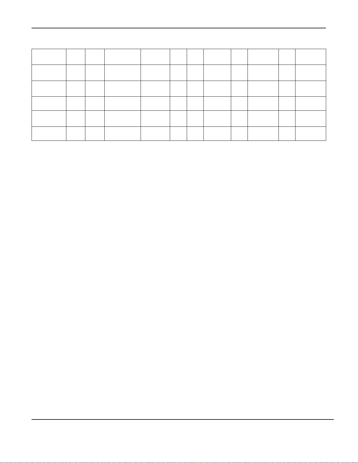
The on-chip dual path filter can be used when the
modulation type is set to Open-Loop VCO or ASK.
Table 18 gives the recommended settings for the
internal component values for various bitrates and
phase detector frequencies. The settings are
calculated to give optimal phase margin for the given
phase-frequency-detector frequency and loop filter
bandwidth. (More values of C and R can be found in
Table 52 and Table 52 on page 40 and 41).
12pF, the same as the varactor input pin
capacitance. C3 can therefore be skipped.
CP_CUR1 CP_CUR0 External Charge Pump Current Internal Charge Pump Current
0 0 12.5µA 1.25/12.5µA
0 1 25µA 3.125/31.25µA
1 0 50µA 6.25/62.5µA
1 1 100µA 12.5/125µA
Table 16. Charge Pump.
April 2006
24
M9999-041906
(408) 955-1690
Page 25
Micrel MICRF405
Mod.
Type
Freq
[MHz]
Baud
Rate
[kbaud/
sec]
Coding
PLL
BW
[kHz]
Phase
margin
[°]
Phase
detector
Freq.
[kHz]
C1
[nF]
C2
[nF]
R1
[kΩ]
R2
[kΩ]
C3
[pF]
VCO All > 30 Manchester 0.8 56 100 10 100 6.2 - VCO All > 100 Manchester 3.0 56 100 0.68 68 27 - -
Divider 315 < 20 DC-free 17 60 500 0.068 6.8 30 75 12
Divider 433 < 20 DC-free 18 60 500 0.068 6.8 30 75 12
Divider 868 < 15 DC-free 20 51 700 0.082 4.7 27 75 18
Divider 915 < 20 DC-free 21 60 500 0.047 4.7 36 91 5.6
Open
loop
All < 200 DC-free 26 56 500 0.047 0.47 43 NC 33000
Table 17. External Loop Filter Values.
CPOUT, p i n 2 0
C2
R1
R2
a)
CP, i nt er n a l
CP, i nt er n a l
Vr e f
VARI N, p i n 2 1
C3C1
R1
C2
CPOUT, pin 20
C1
-
+
c)
C1
C2
R3
R1
VARI N, i n t er na l
C3
VARI N, p i n 2 1
47nF
C3
b)
Figure 11. Loop filter for: a) Closed Loop Modulation, b) Open Loop Modulation and c) Internal Dual Path Filter.
April 2006
25
M9999-041906
(408) 955-1690
Page 26
Micrel MICRF405
Modulation
type
Open loop
VCO
Open loop
VCO
ASK
≤4.8kbps
ASK
≤9.6kbps
ASK
>9.6kbps
Fphd
[kHz]
500 22.5 3.125/31.25 1 32.4 10.8 3 96 7 57 8
1000 45 6.25/62.5 2 32.4 10.8 3 48 2 28 3
1000 32 3.125/31.25 1 32.4 10.8 3 68 4 40 5
2000 64 6.25/62.5 2 32.4 10.8 3 34 1 20 2
2000 220 12.5/125 3 5.4 1.8 0 76 5 5 0
BW
[kHz]
CP
[uA]
Table 18. Internal Dual Path Filter Settings.
CP_CUR
The design of the PLL filter will strongly affect the
performance of the frequency synthesizer. Input
parameters, when designing the loop filter for the
MICRF405, are mainly the modulation method and
the bit rate. Internal loop filter, which have relative
C1
[pF]
C2
[pF]
LF_CAP
R1
[kΩ]
LF_RES1
R3
[kΩ]
high bandwidths, is recommended for ASK. The
external filter must be used when the bandwidth
must be low. These choices will also affect the
switching time and phase noise.
LF_RES3
April 2006
26
M9999-041906
(408) 955-1690
Page 27
Micrel MICRF405
A
A
Modulation
Adr Data
A6..A0 D7 D6 D5 D4 D3 D2 D1 D0
0001011 LowBatt_en=1 Freq_Band1=0 Freq_B and0=1 VCO_freq2=0 VCO_freq1=1 VCO_freq0=1 Modulation1=1 Modulation0=0
0001110 Mod_I4=0 Mod_I3=1 Mod_I2=0 Mod_I1=0 Mod_I0=1 Mod_A2=0 Mod_A1=1 Mod_A0=1
0001111 VCO_Fr_Chk=0 VCO_Fr_Auto=0 FSKn2=1 FSKn1=0 FSKn0=0 Mod_F2=1 Mod_F1=0 Mod_F0=0
0010000 MOD_TEST1=0 Prescaler_Sel=0 FSKClk_K5=1 FSKClk_K4=1 FSKClk_K3=0 FSKClk_K2=1 FSKClk_K1=0 FSKClk_K0=0
0010001 ASK_PN_en=0 ASK_EN=0 ASKshape2=1 ASKshape1=1 ASKshape0=1 ASK2=1 ASK1=1 ASK0=1
0010010 ASKn1=1 ASKn0=0 ASKClk_K5=1 ASKClk_K4=1 ASKClk_K3=0 ASKClk_K2=1 ASKClk_K1=0 ASKClk_K0=0
The frequency modulation can be done in three
different ways with the MICRF405, either by closed-,
open loop VCO modulation or by modulation with
the internal dividers. Amplitude modulation can also
be done in two different ways, either ASK/OOK or
Spread Spectrum ASK™. All these different types of
modulation is selected by Modulation1-0 and
ASK_en (See chapter bit description for details).
Closed loop VCO modulation (Modulation[1:0]=0),
the modulation is applied directly to the VCO. The
PLL will see the modulation as a frequency error and
try to tune the VCO back to carrier. The PLL
bandwidth therefore, needs to be sufficiently low
enough not to cancel the modulation (at least 20
times lower than the slowest variation of the
modulation). Also, the modulation needs to be DCfree, usually by encoding the data by a DC-free code
such as Manchester or 3b4b. In most cases, an
external PLL loop filter must be used to fulfill the
demand for low bandwidth. Please see the
Modulator section for details on deviation and
shaping.
Open Loop VCO Modulation (Modulation[1:0]=1),
modulation is applied directly to the VCO. The VCO
is now left free-running. The varactor voltage will
now be stored on a large external capacitor
connected to the VARIN pin and the PLL is disabled
during the modulation. With the PLL disabled, the
modulation will not be canceled and the modulated
data signal may include DC-components. The
switching between PLL active and disabled is done
automatically by checking the DATAIN pin. If it is tristated the PLL is active, and if it is either high or low
or transitioning between high or low the PLL is then
disabled and the data on the DATAIN pin is
transmitted. When data is transferred through the
SPI the PLL is disabled during the transmission of a
packet, while enabled else. In this mode, the PLL
bandwidth can be fairly high as it is disabled during
transmission. However, due to the large external
capacitor, C3 in Figure 11b), the bandwidth is limited
due to the pole created by this capacitor. Both
internal with 56° phase margin and external filters
are suitable. A high quality capacitor of 10-47nF
(COG type) should be connected on pin VARIN-toground to ensure minimum frequency drift due to
leakage and frequency drift caused by the capacitor
dielectric relaxation phenomenon (25kHz offset after
50ms). For deviation and shaping, please see the
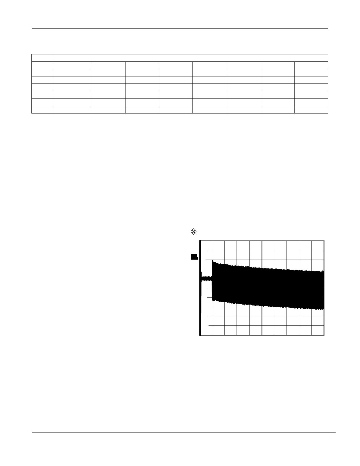
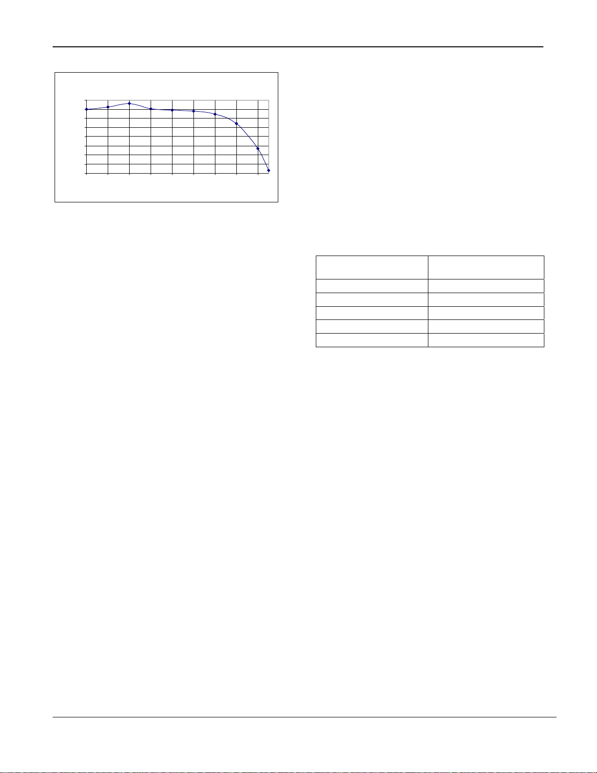
Modulator section. The frequency drift (Hz/ms) over
temperature due to leakage is shown in Figure 12
with a 33nF COG external capacitor.
Figure 13 shows the frequency drift in open loop
VCO modulation due to capacitor dielectric
relaxation. The drift is around 40kHz during a time
period of 50ms. Of the 40kHz drift, 5-10kHz is due to
an initial offset caused by the modulator itself.
*
Ref 0 Hz
160k
120k
1 AP
CLRWR
80k
40k
0
-40k
-80k
-120k
-160k
-200k
-240k
Center 915.00004 MHz 10 ms/
Date: 11.JAN.2006 10:10:03
Figure 12. Frequency Drift Due to Capacitor Dielectric
tt 30 dB
Relaxation at 915MHz.
IFB 10 MHz
QT 100 ms
A
TRG
April 2006
27
M9999-041906
(408) 955-1690
Page 28
Micrel MICRF405
Openloop drift Vdd= 3.6V
100
0
-100
-200
-300
-400
-500
-600
Frequency drift (Hz/ms)
-700
-40 -20 0 20 40 60 80 100 120
Temperature (degC)
Figure 13. Carrier Drift in Open-Loop Modulation.
{PA[2:0]-ASK[2:0]}*3dB. If PA[2:0]<=ASK[2:0], the
ASK modulation will be On Off Keying (OOK). For
example, PA[2:0]=7 and ASK[2:0]=7 is OOK, but if
ASK[2:0]=4, the modulation depth is –9dB (output
power for “1” is 10dBm and “0” is 1dBm). The
modulation depth is a tradeoff between occupied
bandwidth and sensitivity in the receiver. When
increasing the modulation depth, the pulling effect of
the VCO will also increase and can be seen as FM
components in the transmitted signal. To reject the
pulling of the VCO, shaping can be applied to the
ASK signal. The ASKshape[2:0] bits control the
shaping, where ASKshape[2:0] = 7 gives the most
shaping. The shaping is user selectable but a table
Divider Modulation Modulation[1:0]=2, modulation
by switching between two sets of dividers, A0/N0/M0
and A1/N1/M1, is selected. In this case, the PLL
needs to settle at the new frequency for each bitshift. Therefore, the PLL bandwidth needs to be
sufficiently high enough to follow the modulation.
The PLL bandwidth/bit rate ratio controls the filtering
of the modulation. A large ratio gives little filtering
and a square shape to the data; while a small ratio
gives hard filtering of the data. To avoid large
overshoots, a large phase margin is desired, about
70 degrees will give about 10% overshoot. The
tradeoff is less rejection of the phase detector
frequency.
ASK Modulation is selected when ASK_en=1 and
Modulation[2:0]=3. The ASK modulation depth is
controlled by the ASK[2:0] bits, and is equal to
of recommended values is shown in Table 19.
ASK bitrate (kbps)
< 4.8 7
< 9.6 6
< 19.2 4
< 38.4 2
< 50 0
Table 19. Recommended ASK Shaping.
Recommended
ASKshape
A high PLL bandwidth will also help to avoid pulling
of the VCO. The internal third order loop filter should
be selected.
April 2006
28
M9999-041906
(408) 955-1690
Page 29
Micrel MICRF405
A
M
*
1 PK
AXH
Ref 15 dBm
10
D1 1 dBm
0
-10
-20
-30
-40
-50
-60
-70
-80
D2 -19 dBm
tt 50 dB
1
RBW 3 kHz
VBW 10 kHz
SWT 70 ms
1
Marker 1 [T1 ]
-23.62 dBm
915.018000000 MHz
Delta 1 [T1 ]
4.58 dB
-90.000000000 kHz
A
Center 915 MHz Span 600 kHz60 kHz/
Date: 27.MAR.2006 17:23:27
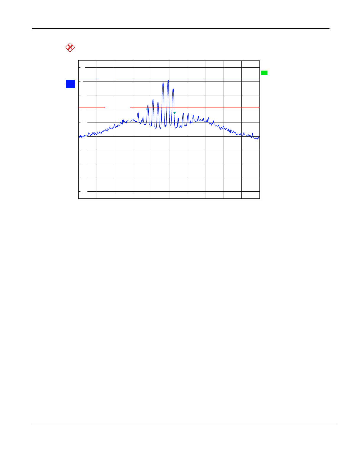
Figure 14. 33kbps, PA=6, ASK=7, ASKshape=2 (Fphd=2MHz, 209kHz internal loop filter).
Spread Spectrum ASK™
is a combination of
traditional ASK combined with FSK dithering. This
modulation type goes under FCC part 15.247 digital
modulation allowing higher output power without
FHSS. The FSK dithering frequency, applied to the
ASK signal, is greater than the ASK data rate and
therefore, a traditional ASK/OOK receiver with
500kHz noise bandwidth can be used. FSK is
applied using divider modulation Modulation[1:0]=2,
due to the high loop filter bandwidth requirement of
the ASK modulation. The ASK_PN_en signal
controls whether the dithering is a “010101”-pattern,
ASK_PN_en=0, or a “111101011001000”-pattern,
ASK_PN_en=1.
April 2006
29
M9999-041906
(408) 955-1690
Page 30
Micrel MICRF405
Bit Rate Settings
The bit rate is set separately for ASK and FSK
modulation to support ASK modulation with FSK
spreading. The FSK bit rate is set with the two
parameters
BR
FSKClk_K and FSKn. The relationship is
f
=
XTAL
KFSKClk
(1)
FSKn
+
3
⋅
2_
where:
BR: Bit rate.
fXTAL: Crystal oscillator frequency.
FSKClk_K: Integer in the range [1..63] (6 bit).
FSKn: Integer in the range [0..5] (3 bit).
A procedure to find the settings for the desired bit
rate is described below:
1. Set FSKn to 0.
2. Calculate FSKClk_K by using this formula:
f
KFSKClk
_
XTAL
=
BR
3
⋅
2
FSKn
+
3. If FSKClk_K is too high, increment FSKn by
one, and then jump to 2.
In some cases, several combinations of FSKClk_K
and FSKn will give the bit rate. If VCO modulation is
selected, Modulation[1:0] < 2, then the lower FSKn
the better shaping of the signal. However in some
cases, low FSKn causes the modulator to saturate
(Please see the section Modulator for details). When
Manchester encoding is enabled, Manchester_en=1,
FSKn needs to bigger than zero for the modulator to
operate properly.
When sending ASK with FSK spreading, FSKClk_K
and FSKn set the speed of the FSK spreading.
The bit rate of the ASK is set similar with the two
parameters ASKClk_K and ASKn. The relationship
is now:
f
BR
=
XTAL
KASKClk
(2)
ASKn
+
5
⋅
2_
where the new parameters are:
ASKClk_K: Integer in the range [1..63] (6 bits).
ASKn: Integer in the range [0..3] (2 bits).
A procedure for finding a bit rate will be equal to
FSK, but with this formula:
f
KASKClk
_
XTAL
=
BR
+
5
⋅
2
ASKn
Due to the high flexibility of the modulator, a brief
explanation of how it works will ease the use of it.
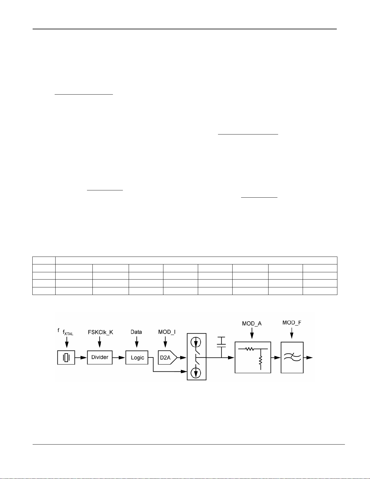
Figure 15 shows a block diagram of the components
of the modulator.
Modulator
Adr Data
A6..A0 D7 D6 D5 D4 D3 D2 D1 D0
0001110 Mod_I4=0 Mod_I3=1 Mod_I2=0 Mod_I1=0 Mod_I0=1 Mod_A2=0 Mod_A1=1 Mod_A0=1
0001111 VCO_Fr_Chk=0 VCO_Fr_Auto=0 FSKn2=1 FSKn1=0 FSKn0=0 Mod_F2=1 Mod_F1=0 Mod_F0=0
0010000 MOD_TEST1=0 Prescaler_Sel=0 FSKClk_K5=1 FSKClk_K4=1 FSKClk_K3=0 FSKClk_K2=1 FSKClk_K1=0 FSKClk_K0=0
Figure 15. Modulator Block Diagram.
April 2006
30
M9999-041906
(408) 955-1690
Page 31

Micrel MICRF405
T
The two first blocks are generating a clock for the
modulator. This clock is, together with the user data,
used to control a charge pump. The charge pump
current is controlled by a DAC. Each time the input
data changes state, a charge is then injected into
the capacitor to generate a modulation signal. The
charge magnitude is controlled by the charging
current and by charging time (inversely proportional
with modulator clock). To be able to achieve small
deviations, it is possible to attenuate the modulation
signal. Finally, the signal is filtered to narrow
transmitter output spectrum.
The procedure is first to determine the settings
concerning the data bit rate, then, these values will
be used in the calculation of the frequency deviation.
Finally, the user must see if the desired values
cause the modulator to saturate.
Deviation Setting
Deviation controlled by user parameters FSKClk_K,
MOD_I, and MOD_A, together with physical
parameters fXTAL and KVCO. All user parameters
can be set in software, and fXTAL (crystal oscillator
frequency) is set when designing in the radio chip.
KVCO (VCO gain) is a parameter of the radio chip,
and is not controllable by the user.
The crystal oscillator frequency, fXTAL, is divided by
FSKClk_K to generate the modulator clock. Since
this modulator clock is controlling the rise and fall
times for the modulator, the frequency deviation is
inversely proportional to this clock. The relationship
is shown in equation (3):
f ∝ (3)
DEV
FSKClk_K
f
XTAL
It is assumed that FSKClk_K will be constant for
most applications to keep bit-rate and shaping
constant, although this is not a requirement.
The primary two controls of frequency deviation are
MOD_I and MOD_A. Of these two, MOD_I is the
Const2 7.54
fC: Carrier frequency of the radio.
FreqBand: Frequency band.
0: 315MHz,
1: 433MHz and
2: 900MHz.
In equation (5), it is evident that the VCO gain is
dependent of carrier frequency. MOD_I is probably
the best parameter to alter if counteracting this effect
if necessary.
Combining equations (3), (4), and (5) gives us an
expression for the frequency deviation:
()()
FreqBandfConstConst
−⋅⋅+
f
DEV
f
XTAL
IMOD
_FSKClk_K
⋅⋅=
AMOD
_
2
−
3
3
C
21
FreqBand
(6)
Observe that equation (6) gives single-sideddeviation. Peak-to-peak deviation is twice this value.
Shaping
The modulation waveform will be shaped due to the
charging and discharging of a capacitor. The
waveform looks like a Gaussian filtered signal with a
Bandwidth⋅Period-product, BT, given by:
B
where:
BT: Shaping factor.
It is evident from this that a low FSKn gives a low
shaping factor, and is thus preferred if it is possible
to choose FSKn freely.
In addition to this, it is possible to smooth the
modulator output in a programmable low-pass filter.
This filter is controlled by the parameter MOD_F.
The parameter should be set according to equation
(8).
FSKn
2= (7)
3
FMOD
≤ (8)
10150_×
BR
parameter that controls the signal generation, while
MOD_A controls attenuation of this signal. The
reason for using an attenuator is to be able to
generate small deviations at high values of
FSKClk_K. The relationship is shown in equation
(4).
IMOD
f
∝ (4)
DEV
Finally, the VCO gain is given by equation (5).
K
=
VCO
_
AMOD
_
2
()()
FreqBandfConstConst
−⋅⋅+
3
C
21
FreqBand
−
3
(5)
where:
9
Const1
106324.30 ×−
April 2006
Modulator Saturation
The modulator output voltage is generated by a
capacitor that is being charged. This means that
there is a risk of saturating the modulator if the
charge received by the capacitor is too large. Use
equation (9) to determine the maximum value of
MOD_I that can be used.
⎛
⎜
IMOD
⎜
⎝
f
XTAL
FSKClk_K
×⋅≤
⎞
6
−
⎟
11028_
+
(9)
⎟
⎠
If it turns out that the MOD_I-range is too small for
your requirements, try increasing FSKn and
decreasing FSKClk_K accordingly.
31
M9999-041906
(408) 955-1690
Page 32

Micrel MICRF405
Lock Detect
Adr Data
A6..A0 D7 D6 D5 D4 D3 D2 D1 D0
0001100 LowBatt_level=0 LDO_by=0 LDO_en1=1 LDO_en0=1 MOD_LDc_en=0 PA_FEc_en=0 PA_LDc_en=0 LD_en=1
0001111 VCO_Fr_Chk=0 VCO_Fr_Auto=0 FSKn2=1 FSKn1=0 FSKn0=0 Mod_F2=1 Mod_F1=0 Mod_F0=0
The lock detector can be enabled by setting
LD_en=1. When pin LD is high, it indicates that the
PLL is in lock. Care must be taken when monitoring
the LD during data transmission using the closed
loop modulation. Due to the fact that the PLL tries to
cancel the modulation signal, there will be some PLL
activity during the transmission time, especially
when the PLL BW is too high relative to the bitrate.
The LD may therefore, show that the PLL is not in
lock.
When starting a transmit session, the LD signal is
helpful in deciding when to turn on the PA. When
going from power down or stand by mode to TX
mode, or after a frequency change, the PLL needs
some time to lock on to the frequency. During this
time it is necessary to keep the PA off. This is done
by setting PA[2:0]=0 and PA_LDc_en=0. When the
LD signal goes high, it is safe to turn on the PA, by
setting the PA[2:0] to the desired output level.
Depending on the output power, and the loop filter,
the LD signal might drop during start up of the PA
due to VCO pulling. When LD is high again it is time
to start the modulation.
The lock detect signal is used internally in several
functions; the VCO_Fr_Chk/Auto, the MOD_LDc and
the PA_LDc. The VCO_Fr_Chk/Auto are described
in detail under the VCO chapter.
PA_LDc (PA Lock Detect Control) is used to
automatically turn on the PA the moment the PLL
has locked on to the frequency. This function is
enabled when the PA_LDc_en bit is set. From power
down or stand by, simply program the MICRF405 to
TX with the wanted PA output setting. The
MICRF405 will then automatically turn on the PA
once the PLL has locked. The PA will remain on until
PA[2:0]=PA_LDc_en=0 or the transmitter leaves
transmit mode (Mode[1:0]<>3). However, the PA is
temporary turned off for every internal load pulse or
if the DATAIN pin is tri-stated in open loop
modulation (Modulation[1:0]=2). This means that if
you want to change frequency, the PA will shut off
during the settling of the new frequency, and then it
is turned on once the PLL has locked on to the new
frequency. It is necessary that LD_en is set for the
PA_LDc function to work.
The correct time to start modulation will be internally
decided when the MOD_LDc (Modulation Lock
Detect control) bit is set. This function is only
working when data is transferred through the SPI
(Bit_IO_en=0). The phase detector frequency (Fphd)
has to be < 200kHz when MOD_LDc is enabled.
Program the MICRF405 in transmit at the proper
output frequency and power strength. Then, write
the frame length of the packet into the data buffer.
The MICRF405 will now delay the modulation until
the PLL has locked with PA turned on. For this
function to work, both LD_en and PA_LDc_en must
be set. This function is especially useful when
transmitting several packets without leaving the TX
mode and the PA_FEc_en bit is set. After a packet
is finished transmitted, the PA_FEc function will turn
the PA off until a new packet is to be sent. If the
MOD_LDc function is not enabled, the modulation
and turning on the PA will then start simultaneously,
there by creating distorted start of packet and
interfering with the settling of the PLL due to PA turn
on. With MOD_LDc enabled the modulation will be
delay until the PLL has locked with PA on.
April 2006
32
M9999-041906
(408) 955-1690
Page 33

Micrel MICRF405
Low Dropout Regulator (LDO) and Low Battery Detector
Adr Data
A6..A0 D7 D6 D5 D4 D3 D2 D1 D0
0001011 LowBatt_en=1 Freq_Band1=0 Freq_B and0=1 VCO_freq2=0 VCO_freq1=1 VCO_freq0=1 Modulation1=1 Modulation0=0
0001100 LowBatt_level=0 LDO_by=0 LDO_en1=1 LDO_en0=1 MOD_LDc_en=0 PA_FEc_en=0 PA_LDc_en=0 LD_en=1
The MICRF405 has three internal LDOs powering
up different parts of the circuit, as can be seen in the
Block Diagram. The output voltages of the LDOs are
around 2.4V. The LDOs can be turned off (default
setting is on) by setting the LDO_en[1:0]=0.
When LDO_en[1:0]=3, the power supply range is
2.2-3.6 volt. Power must be applied to pin 1 and 11.
A capacitor is needed on each of the LDO output for
stability (pin 3, 9 and 23). In sleep mode, all the
LDOs are turned off. The interface and control
blocks run on unregulated power, meaning that the
register content will be kept and that the
programming can also be done in this mode.
An option, where the LDOs are bypassed, is
enabled by setting the LDO_by bit, and when
activated, the transmitter can operate at 2.2V-2.5V.
Since the LDO drop is decreased, the output power
is slightly higher. However, in this mode it is of vital
importance that the input power is below 2.5V as the
pass devices in the LDOs are fully on and not
regulated. It is recommended that this option is used
in combination with the low battery detector.
When LDO_en[1:0]=0, the power supply range is
2.2-2.5 volt. Power must be applied to pin 1, 3, 9, 11
and 23. Capacitors are now only needed for normal
noise decoupling. Alternatively, connect power to
pins 1 and 11 only, and set LDO[1:0]=3 and
LDO_by=0.
The LDOs are controlled with 2 bits, enabling the
option of running the complete circuit on the RF LDO
alone (LDO_en[1:0]=1), or on the RF LDO and
analog LDO (LDO_en[1:0]=2). Doing so, regulated
power on the RFVDD pin must be externally routed
to the AVDD and DVDD pin in the first case and,
and from the RFVDD to the DVDD pin in the second
case. These modes will save one or two of the
external capacitors used for stabilizing the LDOs,
but might influence the phase noise and spurious
performance. Recommended use is therefore,
LDO_en[1:0]=3 or 0.
The low battery detector circuit is turned on when
the LowBatt_en bit is set. It will monitor the voltage
of the input power, pin 11, in standby and TX
modes. If LDO_by=0, it will set the LowBatt interrupt
if the voltages falls below 2.1V for LowBatt_level=1
and 2.0V for LowBatt_level=0. If LDO_by=1, it sets
the interrupt when the voltages is below 1.9V/1.8V
for LowBatt_level=1/0.
April 2006
33
M9999-041906
(408) 955-1690
Page 34
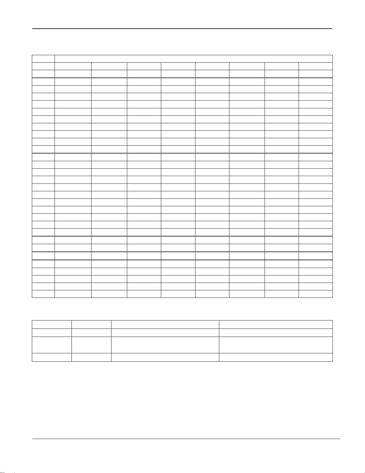
Micrel MICRF405
Bit Description
Adr Data
A6..A0 D7 D6 D5 D4 D3 D2 D1 D0
0000000
0000001
0000010
0000011
0000100
0000101
0000110
0000111
0001000
0001001
0001010
0001011
0001100
0001101
0001110
0001111
0010000
0010001
0010010
0010011
0010100
0010101
0010110
0010111
0011000
0011001
0011010
0011011
0011100
0011101
The 5 last bytes (0011001-0011101) are valid instantly, in other words, no load pulse (raising SEN) is needed to
activate the changes.
Mode1 Mode0 State Comments
Mode1=0 Mode0=1 PA2=1 PA1=1 PA0=1 ClkOut_en=1 Sync_en=1 Load_en=1
- - A0_5=0 A0_4=0 A0_3=1 A0_2=1 A0_1=1 A0_0=0
- - - - N0_11=0 N0_10=0 N0_9=0 N0_8=0
N0_7=0 N0_6=1 N0_5=1 N0_4=1 N0_3=0 N0_2=0 N0_1=1 N0_0=1
- - - - M0_11=0 M0_10=0 M0_9=0 M0_8=0
M0_7=0 M0_6=0 M0_5=1 M0_4=0 M0_3=0 M0_2=0 M0_1=0 M0_0=1
- - A1_5=0 A1_4=1 A1_3=1 A1_2=1 A1_1=1 A1_0=1
- - - - N1_11=0 N1_10=0 N1_9=0 N1_8=0
N1_7=0 N1_6=1 N1_5=1 N1_4=0 N1_3=1 N1_2=1 N1_1=1 N1_0=1
- - - - M1_11=0 M1_10=0 M1_9=0 M1_8=0
M1_7=0 M1_6=0 M1_5=1 M1_4=0 M1_3=0 M1_2=0 M1_1=0 M1_0=0
LowBatt_en=1 Freq_Band1=0 Freq_Band0=1 VCO_freq2=0 VCO_freq1=1 VCO_freq0=1 Modulation1=1 Modulation0=0
LowBatt_level=0 LDO_by=0 LDO_en1=1 LDO_en0=1 MOD_LDc_en=0 PA_FEc_en=0 PA_LDc_en=0 LD_en=1
Bit_IO_en=1 Manchester_en=0 Sel_CRC1=1 Sel_CRC0=1 SyncID_Len1=0 SyncID_Len0=1 Pream_Len1=1 Pream_Len0=0
Mod_I4=0 Mod_I3=1 Mod_I2=0 Mod_I1=0 Mod_I0=1 Mod_A2=0 Mod_A1=1 Mod_A0=1
VCO_Fr_Chk=0 VCO_Fr_A uto=0 FSKn2=1 FSKn1=0 FSKn0=0 Mod_F2=1 Mod_F1=0 Mod_F0=0
‘0’ Prescaler_Sel=0 FSKClk_K5=1 FSKClk_K4=1 FSKClk_K3=0 FSKClk_K2=1 FSKClk_K1=0 FSKClk_K0=0
ASK_PN_en=0 ASK_EN=0 ASKshape2=1 ASKshape1=1 ASKshape0=1 ASK2=1 ASK1=1 ASK0=1
ASKn1=1 ASKn0=0 ASKClk_K5=1 ASKClk_K4=1 ASKClk_K3=0 ASKClk_K2=1 ASKClk_K1=0 ASKClk_K0=0
INT_LF_EN=1 CP_CUR1=0 CP_CUR0=1 LF_RES1_4=0 LF_RES1_3=1 LF_RES1_2=0 LF_RES1_1=0 LF_RES1_0=1
LF_High_PM=1 LF_CAP1=1 LF_CAP0=1 LF_RES3_4=0 LF_RES3_3=0 LF_RES3_2=1 LF_RES3_1=0 LF_RES3_0=1
ClkOut_1=0 ClkOut_0=0 XCO_Fast= 1 XCOtune4=1 XCOtune3=0 XCOtune2=0 XCOtune1=0 XCOtune0=0
INT_LF_TEST=0 VCO_IB2=0 VCO_IB1=0 VCO_IB0=0 VCO_by=0 OUTS2=0 OUTS1=0 OUTS0=0
PA_IB3=1 PA_IB2 =0 PA_IB1=0 PA_IB0=1 PAB_IB3=1 PAB_IB2=0 PAB_IB1=0 PAB_IB0=1
VCO_freq_O2 VCO_freq_O1 VCO_freq_O0 VC_HI VC_LO LOW_BATT
SyncID3_7=1 SyncID3_6=1 SyncID3_5=1 SyncID3_4=0 SyncID3_3=0 SyncID3_2=1 SyncID3_1=0 SyncID3_0=1
SyncID2_7=1 SyncID2_6=1 SyncID2_5=1 SyncID2_4=0 SyncID2_3=0 SyncID2_2=1 SyncID2_1=0 SyncID2_0=1
SyncID1_7=1 SyncID1_6=1 SyncID1_5=1 SyncID1_4=0 SyncID1_3=0 SyncID1_2=1 SyncID1_1=0 SyncID1_0=1
SyncID0_7=1 SyncID0_6=1 SyncID0_5=1 SyncID0_4=0 SyncID0_3=0 SyncID0_2=1 SyncID0_1=0 SyncID0_0=1
DATA_7 DATA_6 DATA_5 DATA_4 DATA_3 DATA_2 DATA_1 DATA_0
0 0 Power down Keeps Register configuration
0
1
1
0
Standby Crystal Oscillator running
1 1 Transmit mode Transmit mode
Table 20. Main Mode.
April 2006
34
M9999-041906
(408) 955-1690
Page 35
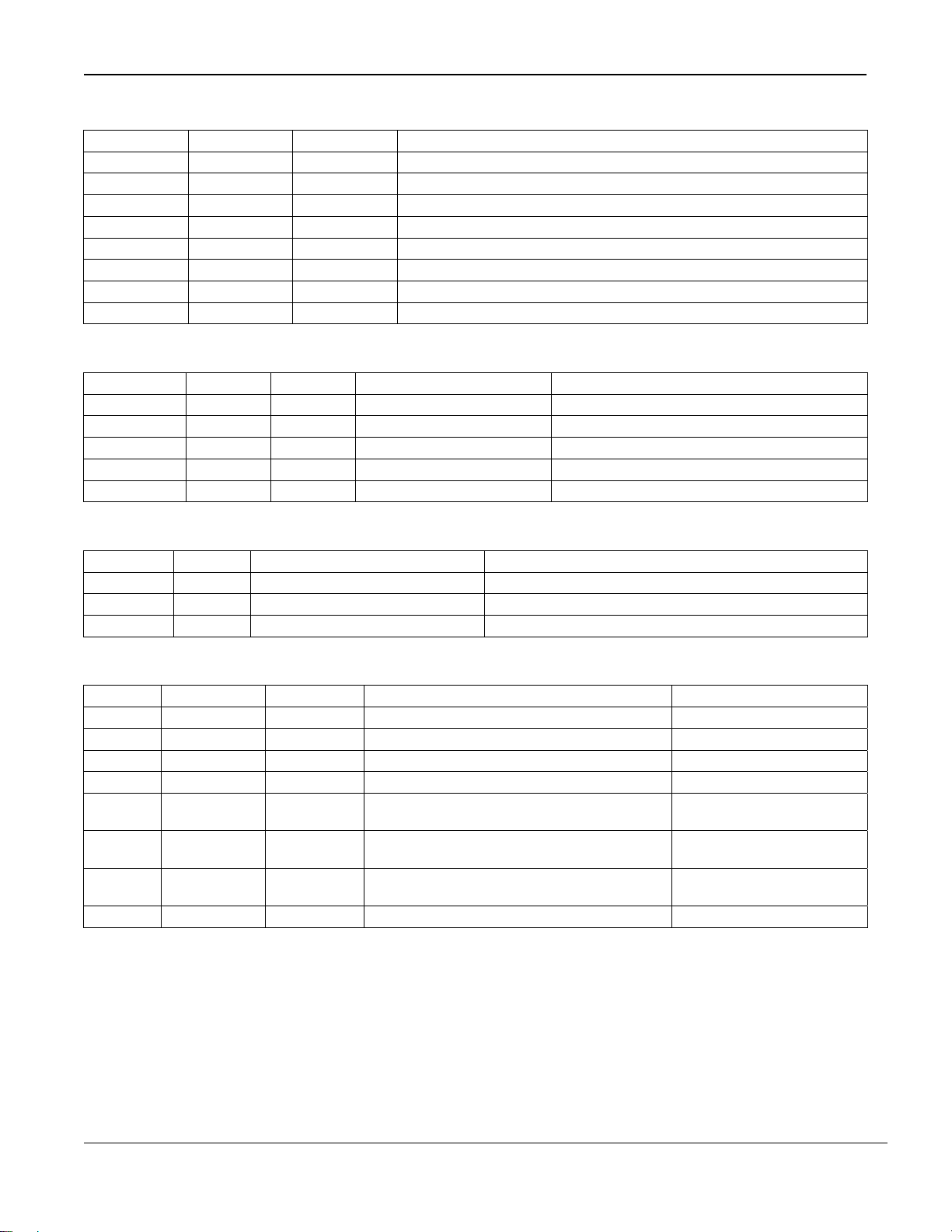
Micrel MICRF405
A
A
A
PA2 PA1 PA0 State
0 0 0 21dB attenuation or PA off if PA_LDc_en=0
0 0 1 18dB attenuation
0 1 0 15dB attenuation
0 1 1 12dB attenuation
1 0 0 9dB attenuation
1 0 1 6dB attenuation
1 1 0 3dB attenuation
1 1 1 Max output
Table 21. Power Amplifier.
ClkOut_en ClkOut_1 ClkOut_0 State Comments
0 X X CLKOUT off Output is 0 volt.
1 0 0 CLKOUT on The XCO frequency is divided by 16.
1 0 1 CLKOUT on The XCO frequency is divided by 8.
1 1 0 CLKOUT on The XCO frequency is divided by 4.
1 1 1 CLKOUT on The XCO frequency is divided by 2.
Table 22. Output Clock.
Bit_IO_en Sync_en State Comments
0 X DCLK pin on, RDY Byte ready, RDY, signal from databyte
1 0 DCLK pin off Transparent transmission of data
1 1 DCLK pin on, DATACLK Bit-clock is generated by transmitter
Table 23. Synchronizer Mode
ASK_EN Modulation1 Modulation0 State Comments
0 0 0 Closed loop VCO-modulation VCO is phase-locked
0 0 1 Open loop VCO-modulation VCO is free-running
0 1 0 Modulation by A,M and N Modulation inside PLL
0 1 1 Not used
1 0 0
1 0 1
1 1 0
1 1 1 ASK modulation VCO is phase-locked
SK modulation with spreading code applied to
VCO. Not recommended.
SK modulation with spreading code applied to
VCO. Not recommended.
SK modulation with spreading code applied to
internal modulation by A, M and M
Table 24. Modulation.
VCO is phase-locked
VCO is free-running
Modulation inside PLL
April 2006
35
M9999-041906
(408) 955-1690
Page 36
Micrel MICRF405
ASK2 ASK1 ASK0 State
0 0 0 3dB ASK depth
0 0 1 6dB ASK depth
0 1 0 9dB ASK depth
0 1 1 12dB ASK depth
1 0 0 15dB ASK depth
1 0 1 18dB ASK depth
1 1 0 21dB ASK depth
1 1 1 > 30dB ASK depth
Table 25. ASK Modulation Depth When PA[2:0]=7.
ASKshape Comments
0..7 Programmable ASK filter. It can be programmed in eight steps. “0” is no shaping, “7” most shaping.
Table 26. ASK Shaping/Filtering.
XCOtune Comments
0..31 Programmable XCO load capacitor
Table 27. XCO Capacitor Setting.
XCO_Fast Comments
0 The XCO is running on a constant bias current.
1 When going from PD to TX mode, the XCO is running on a high current during start up.
Table 28. XCO Fast Startup.
Low_Batt_en LowBatt_level LDO_by Comments
0 X X Low battery detect circuit off
1 0 0
1 1 0
1 0 1
1 1 1
Low battery detect circuit active. Interrupt is flagged if VDD falls below
2V.
Low battery detect circuit active. Interrupt is flagged if VDD falls below
2.1V.
Low battery detect circuit active. Interrupt is flagged if VDD falls below
1.8V.
Low battery detect circuit active. Interrupt is flagged if VDD falls below
1.9V.
Table 29. Low Battery Detect.
April 2006
36
M9999-041906
(408) 955-1690
Page 37
Micrel MICRF405
LDO_by LDO_EN1 LDO_EN0 Comments
X 0 0
1 X X LDOs bypassed, power applied to the VDD pin1 and VDD pin11, min/max is 2.0/2.5 V
0 0 1
0 1 0
0 1 1
PA_LDc_en Comments
0 PA is only controlled by Mode1 and Mode and PA0-2, PA on in transmit mode (Mode[1:0]=3 and PA[2:0]>0)
In transmit mode, PA is turned on by Lock Detect (LD=1 -> PA on). PA is turned off by load pulse or when
1
MOD_LDc_en Comments
0 Modulation starts once frame length is written into data byte.
1 Modulation starts once frame length is written into data byte and PA is turned on and LD is high.
using openloop modulation and setting the DATAIN pin in tri-state. PA will be turned on again once LD goes
high again. LD_en must be set to 1.
Table 32. Lock Detect Controlled Start of Modulation (only for BIT_IO_en=0).
LDOs turned off, power applied to AVDD, DVDD, RFVDD, min/max is 2.0/2.5 V, and
to VDD pin 11 and 1, min/max is 2.0/3.6V.
PA LDO turned on, power applied to VDD pin1 and 11, min/max is 2.0/3.6V, and to
AVDD and DVDD, min/max is 2.0/2.5V
PA and AVDD LDO turned on, power applied to the VDD pin1 and 11, min/max is
2.0/3.6V, and to DVDD, min/max is 2.0/2.5V
PA, AVDD and DIG LDO turned on, power applied to the VDD pin1 and VDD pin 11,
min/max is 2.0/3.6V
Table 30. Low DropOut Voltage Regulator.
Table 31. Lock Detect Controlled PA.
PA_FEc_en Comments
0 PA is turned off by Mode1 and Mode0 or PA0-2 and PA_LDc_en=0
1 PA is turned off immediately after the frame is transmitted.
Table 33. Frameend Controlled PA.
LD_en State Comments
0 LD off Output is 0 volt, or test signals specified by OUTS[2:0]
1 LD on LD pin high indicate that the PLL is locked
Table 34. Lock Detector.
SyncID_Len1 SyncID_Len0 Comments
0 0 SyncID length is 1 byte. SyncID0 is sent
0 1 SyncID length is 2 bytes. SyncID0 and SyncID1 is sent
1 0 SyncID length is 3 bytes. SyncID0, SyncID1 and SyncID2 is sent
1 1 SyncID length is 4 bytes. SyncID0, SyncID1, SyncID2 and SyncID3 is sent.
Table 35. SyncID Field Length.
April 2006
37
M9999-041906
(408) 955-1690
Page 38
Micrel MICRF405
Pream_Len1 Pream_Len0 Comments
0 0 Preamble length is 1 byte.
0 1 Preamble length is 2 bytes.
1 0 Preamble length is 3 bytes.
1 1 Preamble length is 4 bytes.
Table 36. Preamble Field Length.
Sel_CRC1 Sel_CRC0 Comments
0 X CRC disabled
1 0
1 1
Manchester_en Comments
0 Manchester encoding disabled.
Manchester encoding enabled. Data will be encoded before transmitted.
1
VCO_freq2 VCO_freq1 VCO_freq0 Comments
0 0 0 Not used
0 0 1
0 1 0 868 MHz, 433MHz
0 1 1
1 0 0 915 MHz
1 0 1
1 1 0 950MHz, 315MHz
1 1 1
FSKn > 0 when using modulator.
CCITT-8 CRC enabled. Byte is sent after payload data.
Polynomial function: X^8+X^5+X^4+1. (Byte part of Frame Length)
ITU-16 CRC enabled. Bytes are sent after payload data.
Polynomial function: X^16+X^12+X^5+1. (Byte part of Frame Length)
Table 37. CRC Select.
Table 38. Manchester Encoding (only when BIT_IO_en=0).
Table 39. VCO Frequency.
MOD_I Comments
1..31 The deviation is linearly dependent of MOD_I
Table 40. Modulator Current Setting for Frequency Deviation.
MOD_A Comments
Frequency deviation attenuator (or range selector). The attenuations are (values 0 through 4, respectively)
0..4
1
1
1
,
1
,
2
1
,
4
8
Table 41. Modulator Attenuator Setting for Frequency Deviation.
and
1
16
April 2006
38
M9999-041906
(408) 955-1690
Page 39
Micrel MICRF405
MOD_F Comments
0..3
Programmable smoothing filter after attenuator. This can be programmed in four steps, and will produce
reasonable results for the highest bit rates.
Table 42. Modulator Filter Setting.
FSKn Comments
0..5 The bit rate clock is set by dividing the crystal oscillator frequency by FSKClk_K*2^(3+FSKn).
Table 43. Bit Rate Setting.
FSKClk_K Comments
1..63
The crystal oscillator is divided by this number to produce modulator clock and it is divided further down by
2^(3+FSKn) to produce the bit rate clock.
Table 44. Modulator and Bit Rate Clock Setting.
ASKn Comments
0..3 The ASK bitrate clock is set by dividing the crystal oscillator frequency by ASKClk_K*2^(5+ASKn)
Table 45. Bit Rate Setting.
ASKClk_K Comments
1..63
The crystal oscillator is divided by this number and is divided further down by 2^(5+ASKn) to produce the
ASK bitrate clock.
Table 46. Modulator and Bit Rate Clock Setting.
ASK_PN_en Comments
0 01010101…pattern is used in the FSK spreader during ASK.
1 111101011001000 repeated pattern is used in the FSK spreader during ASK.
Table 47. ASK Spreading.
VCO_IB2 VCO_IB1 VCO_IB0 Comments
1 1 1 Bias setting for VCO_Freq=0/1, 860 MHz
1 0 1 Bias setting for VCO_Freq=2/3, 868 MHz
0 1 1 Bias setting for VCO_Freq=4/5, 915 MHz
0 0 0 Bias setting for VCO_Freq=6/7, 950 MHz (**)
(**): When VCO_IB=000b, the bias current is set automatically by the two VCO_freq bit.
Table 48. VCO Bias Bit.
VCO_by State Comment
0 VCO is active
1 VCO is bypassed
When VCO is bypassed, a differential signal can be applied to the circuit using
pin CPOUT and VARIN
Table 49. VCO Bypass Bit.
April 2006
39
M9999-041906
(408) 955-1690
Page 40
Micrel MICRF405
OutS2 OutS1 OutS0 The signals are available on the LD output
0 0 0 Gnd
0 0 1 N-div
0 1 0 M-div
0 1 1 ModOut
1 0 0 Bandgap
1 0 1
1 1 0 DVDD
1 1 1 TXSYMBOL – output of packet handling engine
Table 50. Test Signals. Only Available When LD_en=0.
PA_IB3 PA_IB2 State
0 0 PA uses bias current from PTAT bias source, external resistor (Pin 6)
0 1 PA uses bias current from CI bias source, external resistor (Pin 24)
1 0 PA uses bias current from internal bias source, PTAT
1 1 PA uses bias current from internal bias source, PTAT + CI
PA_IB1 PA_IB0 State
0 0 PA bias current setting, lowest bias current
0 1 PA bias current setting
1 0 PA bias current setting
1 1 PA bias current setting, highest bias current
PAB_IB3 PAB_IB2 State
0 0 PAbuffer uses bias current from PTAT bias source, external resistor (Pin 6)
0 1 PAbuffer uses bias current from CI bias source, external resistor (Pin 24)
1 0 PAbuffer uses bias current from internal bias source, PTAT
1 1 PAbuffer uses bias current from internal bias source, PTAT + CI
PAB_IB1 PAB_IB0 State
0 0 PAbuffer bias current setting, lowest bias current
0 1 PAbuffer bias current setting
1 0 PAbuffer bias current setting
1 1 PAbuffer bias current setting, highest bias current
Table 51. PA and PAbuffer Bias Current Setting.
LF_High_PM LF_CAP1 LF_CAP0 C1 C2
X 0 0 5.4pF 1.8pF
0 0 1 10.8pF 3.6pF
0 1 0 21.6pF 7.2pF
0 1 1 32.4pF 10.8pF
1 0 1 10.8pF 1.8pF
1 1 0 21.6pF 3.6pF
1 1 1 32.4pF 5.4pF
Table 52. Loop Filter Capacitors Values.
April 2006
40
Max. achievable Phase
Margin
57°
57°
57°
57°
69°
69°
69°
M9999-041906
(408) 955-1690
Page 41
Micrel MICRF405
LF_RES1<4:0>
LF_RES3<4:0> R1 (kΩ) R3 (kΩ)
0 24.1 5.9
1 34.3 12.3
2 44.5 18.7
3 54.7 25.1
4 64.9 31.5
5 75.1 37.9
6 85.3 44.3
7 95.5 50.7
8 105.7 57.1
9 115.9 63.5
10 126.1 69.9
11 136.3 76.3
12 146.5 82.7
13 156.7 89.1
14 166.9 95.5
15 177.1 101.9
16 187.3 108.3
17 197.5 114.7
18 207.7 121.1
19 217.9 127.5
20 228.1 133.9
21 238.3 140.3
22 248.5 146.7
23 258.7 153.0
24 268.9 159.4
25 279.1 165.8
26 289.3 172.2
27 299.5 178.6
28 309.7 185.0
29 319.9 191.4
30 330.1 197.8
31 340.4 204.2
Table 53. Loop Filter Resistor Values.
April 2006
41
M9999-041906
(408) 955-1690
Page 42
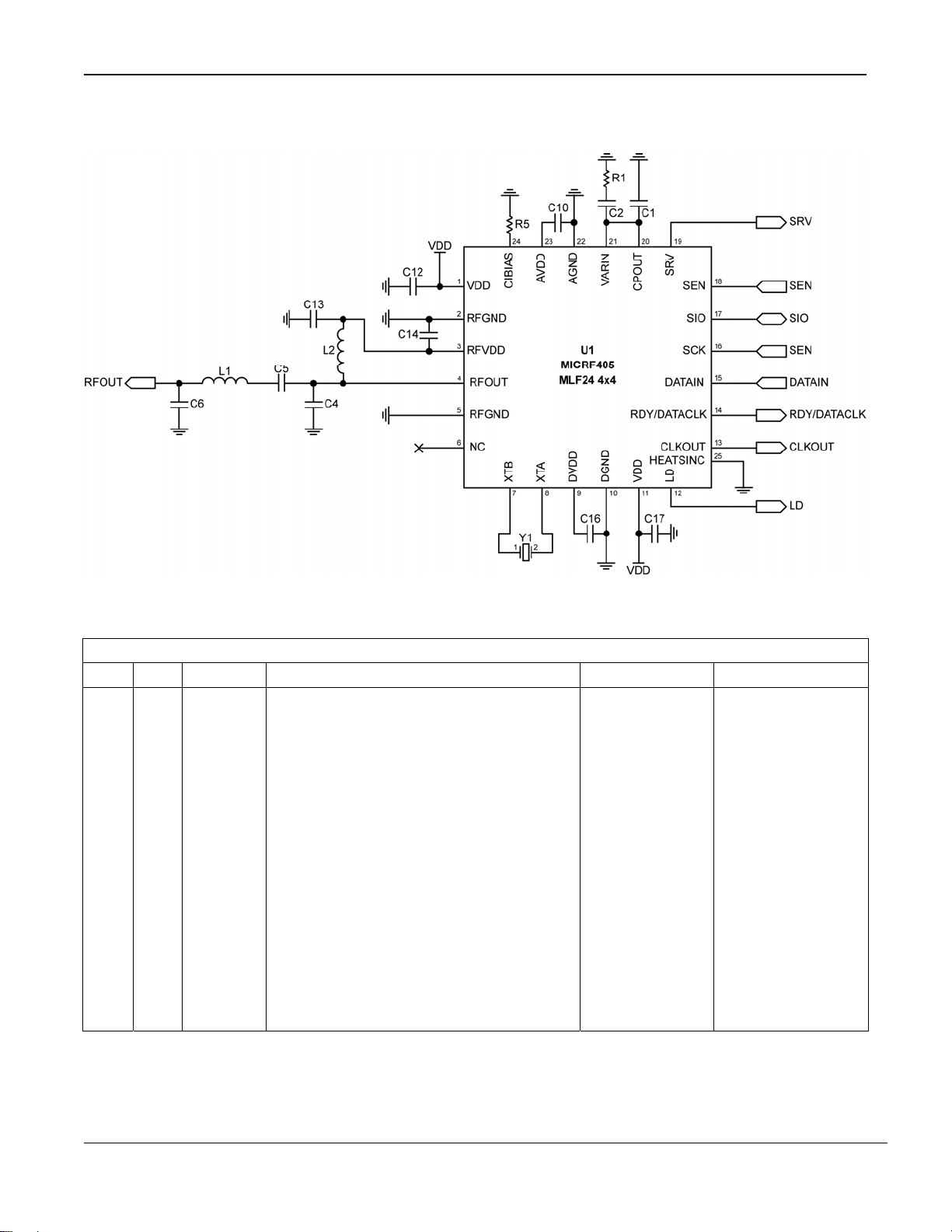
Micrel MICRF405
Typical Application Circuit
Figure 16. Typical Application Circuit
Bill of Materials
FSK/ASK 915MHz
Item Part Value Description Manufacturer Part Number
1 C1 - See Table 17
2 C2 - See Table 17
3 C4 3p3 Capacitor, 0603, ±0.25pF, COG, 50V, -55,+125°C Kyocera CM105CG3R3C50A
4 C5 100pF Capacitor, 0603, ±5%, COG, 50V, -55,+85°C Kyocera CM105CG101J50A
5 C6 3p3 Capacitor, 0603, ±0.25pF, COG, 50V, -55,+125°C Kyocera CM105CG3R3C50A
6 C10 100nF Capacitor, 0603, ±10%, X7R, 16V, -55,+125°C Kyocera CM105X7R104K16A
7 C12 10nF Capacitor, 0603, ±10%, X7R, 50V, -55,+125°C Kyocera CM105X7R103K50A
8 C13 100nF Capacitor, 0603, ±10%, X7R, 16V, -55,+125°C Kyocera CM105X7R104K16A
9 C14 100nF Capacitor, 0603, ±10%, X7R, 16V, -55,+125°C Kyocera CM105X7R104K16A
10 C16 100nF Capacitor, 0603, ±10%, X7R, 16V, -55,+125°C Kyocera CM105X7R104K16A
11 C17 10nF Capacitor, 0603, ±10%, X7R, 50V, -55,+125°C Kyocera CM105X7R103K50A
12 R1 - See Table 17
13 R5 82k Resistor, 0603, ±1%, 50V, -55,+125°C Kyocera CR10-8202F
14 L1 10nH Inductor, 0603, ±5%, -40,+125°C Coilcraft 0603CS-10NXJB
15 L2 12nH Inductor, 0603, ±5%, -40,+125°C Coilcraft 0603CS-12NXJB
16 Y1 16MHz Crystal, TSX-10A, ±10ppm, -20,+75°Cl Toyocom TN4-26011
April 2006
42
M9999-041906
(408) 955-1690
Page 43
Micrel MICRF405
FSK/ASK 868MHz
Item Part Value Description Manufacturer Part Number
1 C1 - See Table 17
2 C2 - See Table 17
3 C4 3p9 Capacitor, 0603, ±0.25pF, COG, 50V, -55,+125°C Kyocera CM105CG3R9C50A
4 C5 15pF Capacitor, 0603, ±5%, COG, 50V, -55,+85°C Kyocera CM105CG150J50A
5 C6 6p8 Capacitor, 0603, ±0,5pF, COG, 50V, -55,+125°C Kyocera CM105CG6R8D50A
6 C10 100nF Capacitor, 0603, ±10%, X7R, 16V, -55,+125°C Kyocera CM105X7R104K16A
7 C12 10nF Capacitor, 0603, ±10%, X7R, 50V, -55,+125°C Kyocera CM105X7R103K50A
8 C13 100nF Capacitor, 0603, ±10%, X7R, 16V, -55,+125°C Kyocera CM105X7R104K16A
9 C14 100nF Capacitor, 0603, ±10%, X7R, 16V, -55,+125°C Kyocera CM105X7R104K16A
10 C16 100nF Capacitor, 0603, ±10%, X7R, 16V, -55,+125°C Kyocera CM105X7R104K16A
11 C17 10nF Capacitor, 0603, ±10%, X7R, 50V, -55,+125°C Kyocera CM105X7R103K50A
12 R1 - See Table 17
13 R5 82k Resistor, 0603, ±1%, 50V, -55,+125°C Kyocera CR10-8202F
14 L1 10nH Inductor, 0603, ±5%, -40,+125°C Coilcraft 0603CS-10NXJB
15 L2 12nH Inductor, 0603, ±5%, -40,+125°C Coilcraft 0603CS-12NXJB
16 Y1 16MHz Crystal, TSX-10A, ±10ppm, -20,+75°Cl Toyocom TN4-26011
FSK/ASK 433MHz
Item Part Value Description Manufacturer Part Number
1 C1 - See Table 17
2 C2 - See Table 17
3 C4 5p6 Capacitor, 0603, ±0,5pF COG, 50V, -55,+125°C Kyocera CM105CG5R6D50A
4 C5 6p8 Capacitor, 0603, ±0,5pF, COG, 50V, -55,+85°C Kyocera CM105CG6R8D50A
5 C6 6p8 Capacitor, 0603, ±0,5pF, COG, 50V, -55,+125°C Kyocera CM105CG6R8D50A
6 C10 100nF Capacitor, 0603, ±10%, X7R, 16V, -55,+125°C Kyocera CM105X7R104K16A
7 C12 10nF Capacitor, 0603, ±10%, X7R, 50V, -55,+125°C Kyocera CM105X7R103K50A
8 C13 100nF Capacitor, 0603, ±10%, X7R, 16V, -55,+125°C Kyocera CM105X7R104K16A
9 C14 100nF Capacitor, 0603, ±10%, X7R, 16V, -55,+125°C Kyocera CM105X7R104K16A
10 C16 100nF Capacitor, 0603, ±10%, X7R, 16V, -55,+125°C Kyocera CM105X7R104K16A
11 C17 10nF Capacitor, 0603, ±10%, X7R, 50V, -55,+125°C Kyocera CM105X7R103K50A
12 R1 - See Table 17
13 R5 82k Resistor, 0603, ±1%, 50V, -55,+125°C Kyocera CR10-8202F
14 L1 47nH Inductor, 0603, ±5%, -40,+125°C Coilcraft 0603CS-47NXJB
15 L2 47nH Inductor, 0603, ±5%, -40,+125°C Coilcraft 0603CS-47NXJB
16 Y1 16MHz Crystal, TSX-10A, ±10ppm, -20,+75°Cl Toyocom TN4-26011
April 2006
43
M9999-041906
(408) 955-1690
Page 44
Micrel MICRF405
FSK/ASK 315MHz
Item Part Value Description Manufacturer Part Number
1 C1 - See Table 17
2 C2 - See Table 17
3 C4 10p Capacitor, 0603, ±5%, COG, 50V, -55,+125°C Kyocera CM105CG100J50A
4 C5 100pF Capacitor, 0603, ±5%, COG, 50V, -55,+85°C Kyocera CM105CG101J50A
5 C6 10p Capacitor, 0603, ±5%, COG, 50V, -55,+125°C Kyocera CM105CG100J50A
6 C10 100nF Capacitor, 0603, ±10%, X7R, 16V, -55,+125°C Kyocera CM105X7R104K16A
7 C12 10nF Capacitor, 0603, ±10%, X7R, 50V, -55,+125°C Kyocera CM105X7R103K50A
8 C13 100nF Capacitor, 0603, ±10%, X7R, 16V, -55,+125°C Kyocera CM105X7R104K16A
9 C14 100nF Capacitor, 0603, ±10%, X7R, 16V, -55,+125°C Kyocera CM105X7R104K16A
10 C16 100nF Capacitor, 0603, ±10%, X7R, 16V, -55,+125°C Kyocera CM105X7R104K16A
11 C17 10nF Capacitor, 0603, ±10%, X7R, 50V, -55,+125°C Kyocera CM105X7R103K50A
12 R1 - See Table 17
13 R5 82k Resistor, 0603, ±1%, 50V, -55,+125°C Kyocera CR10-8202F
14 L1 47nH Inductor, 0603, ±5%, -40,+125°C Coilcraft 0603CS-47NXJB
15 L2 47nH Inductor, 0603, ±5%, -40,+125°C Coilcraft 0603CS-47NXJB
16 Y1 16MHz Crystal, TSX-10A, ±10ppm, -20,+75°Cl Toyocom TN4-26011
April 2006
44
M9999-041906
(408) 955-1690
Page 45
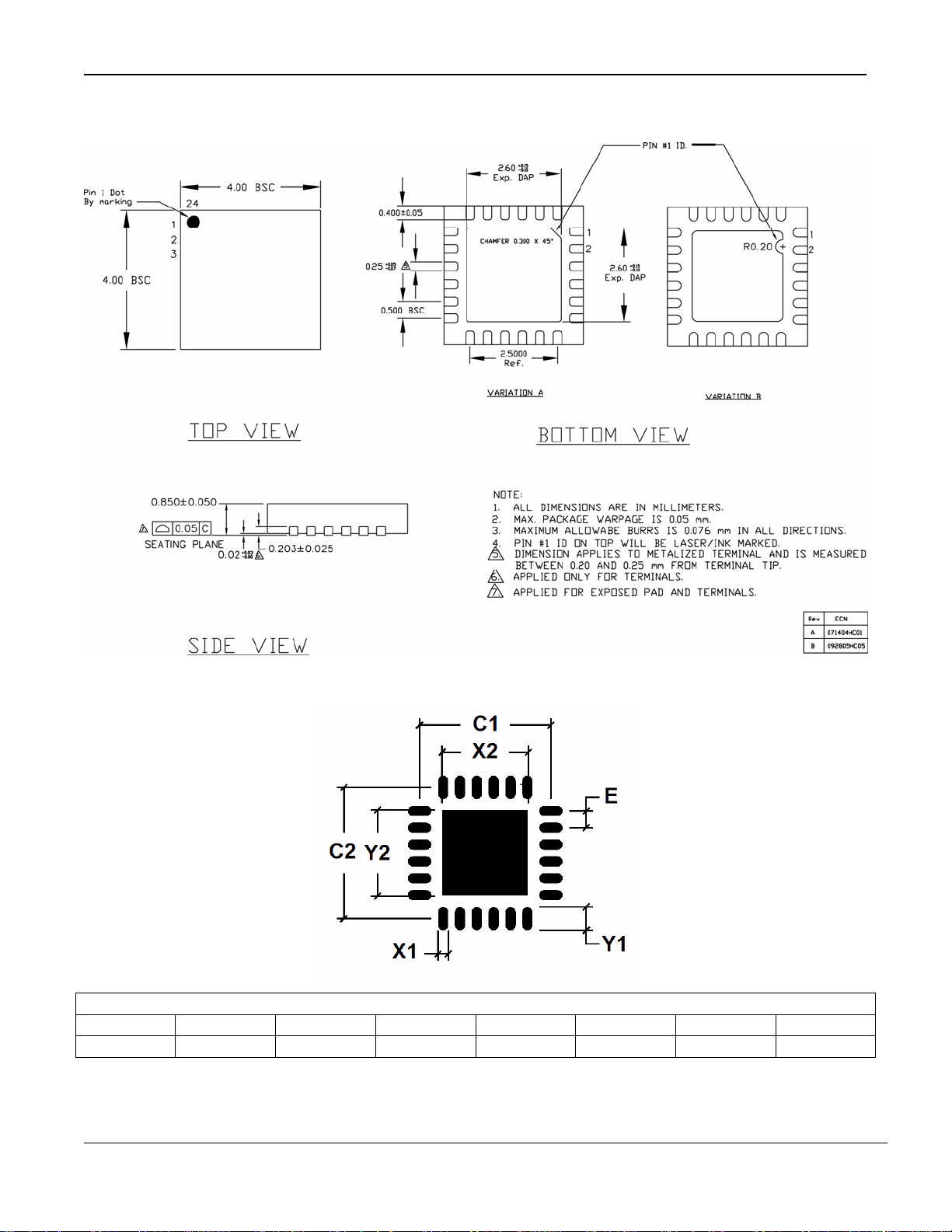
Micrel MICRF405
Package Information
24-Lead MLF® (ML)
MLF® 4 4x4mm Land pattern
E X1 Y1 C1 C2 X2 Y2
Min
0.50 0.30 0.70 3.90 3.90 2.55 2.55
April 2006
45
M9999-041906
(408) 955-1690
Page 46

Micrel MICRF405
MICREL, INC. 2180 FORTUNE DRIVE SAN JOSE, CA 95131 USA
TEL +1 (408) 944-0800 FAX +1 (408) 474-1000 WEB http:/www.micrel.com
The information furnished by Micrel in this data sheet is believed to be accurate and reliable. However, no responsibility is assumed by Micrel
for its use. Micrel reserves the right to change circuitry and specifications at any time without notification to the customer.
Micrel Products are not designed or authorized for use as components in life support appliances, devices or systems where malfunction of a
product can reasonably be expected to result in personal injury. Life support devices or systems are devices or systems that (a) are intended
for surgical implant into the body or (b) support or sustain life, and whose failure to perform can be reasonably expected to result in a
significant injury to the user. A Purchaser’s use or sale of Micrel Products for use in life support appliances, devices or systems is a
Purchaser’s own risk and Purchaser agrees to fully indemnify Micrel for any damages resulting from such use or sale.
April 2006
© 2006 Micrel, Incorporated.
46
M9999-041906
(408) 955-1690
 Loading...