


74LV14
Hex inverting Schmitt trigger
Rev. 6 — 12 December 2011 Product data sheet
1. General description
The 74L V14 is a low-voltage Si-gate CM OS device that is pin and function comp atible with
74HC14 and 74HCT14.
The 74LV14 provides six inverting buffers with Schmitt-trigger input. It is capable of
transforming slowly-changing input signals into sharply defined, jitter-free output signals.
The inputs switch at different point s for positive and negative-going signals. The dif ference
between the positive voltage V
hysteresis voltage V
2. Features and benefits
Wide operating voltage: 1.0 V to 5.5 V
Optimized for low voltage applications: 1.0 V to 3.6 V
Accepts TTL input levels between V
Typical output ground bounce < 0.8 V at V
Typical HIGH-level output voltage (V
T
= 25 C
amb
ESD protection:
HBM JESD22-A114F exceeds 2000 V
MM JESD22-A115-A exceeds 200 V
Multiple package options
Specifie d from 40 Cto+85C and from 40 Cto+125C
and the negative voltage VT is defined as the input
T+
.
H
= 2.7 V and VCC = 3.6 V
CC
= 3.3 V and T
CC
) undershoot: > 2 V at VCC = 3.3 V and
OH
amb
= 25 C
3. Applications
Wave and pulse shapers for highly noisy environments
Astable multivibrators
Monostable multivibrators

NXP Semiconductors
mna204
1A 1Y
1
2
2A 2Y
3
4
3A 3Y
5
6
4A 4Y
9
8
5A 5Y
11
10
6A 6Y
13
12
8
9
10
11
001aac497
12
13
2
1
4
3
6
5
mna025
A
Y
4. Ordering information
74LV14
Hex inverting Schmitt trigger
Table 1. Ordering information
Type number Package
Temperature range Name Description Version
74LV14N 40 Cto+125C DIP14 plastic dual in-line package; 14 leads (300 mil) SOT27-1
74LV14D 40 Cto+125C SO14 plastic small outline package; 14 leads;
SOT108-1
body width 3.9 mm
74LV14DB 40 Cto+125C SSOP14 plastic shrink small outline package; 14 leads;
SOT337-1
body width 5.3 mm
74LV14PW 40 Cto+125C TSSOP14 plastic thin shrink small outline package; 14 leads;
SOT402-1
body width 4.4 mm
74LV14BQ 40 Cto+125C DHVQFN14 plastic dual in-line compatible thermal enhanced very
SOT762-1
thin quad flat package; no leads; 14 terminals;
body 2.5 3 0.85 mm
5. Functional diagram
Fig 1. Logic symbol Fig 2. IEC logic symbol Fig 3. Logic diagram for one
Schmitt trigger
74LV14 All information provided in this document is subject to legal disclaimers. © NXP B.V. 2011. All rights reserved.
Product data sheet Rev. 6 — 12 December 2011 2 of 19
NXP Semiconductors
74LV14
1A V
CC
1Y 6A
2A 6Y
2Y 5A
3A 5Y
3Y 4A
GND 4Y
001aah095
1
2
3
4
5
6
7
8
10
9
12
11
14
13
001aah096
74LV14
Transparent top view
V
CC
(1)
3Y 4A
3A 5Y
2Y 5A
2A 6Y
1Y 6A
GND
4Y
1A
V
CC
6 9
5 10
4 11
3 12
2 13
7
8
1
14
terminal 1
index area
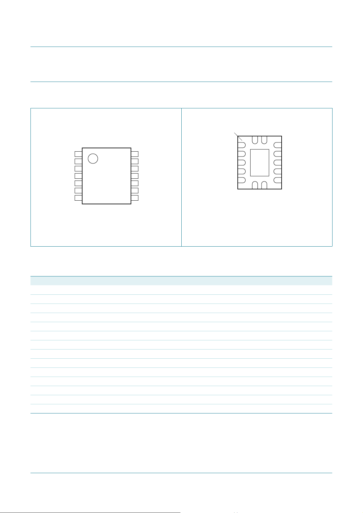
6. Pinning information
6.1 Pinning
74LV14
Hex inverting Schmitt trigger
(1) The die substrate is attached to the exposed die pad
using conductive die attach material. It can not be
used as a supply pin or input.
Fig 4. Pin configuration DIP14, SO14 and (T)SSOP14 Fig 5. Pin configuration DHVQFN14
6.2 Pin description
Table 2. Pin description
Symbol Pin Description
1A 1 data input
1Y 2 data output
2A 3 data input
2Y 4 data output
3A 5 data input
3Y 6 data output
GND 7 ground (0 V)
4Y 8 data output
4A 9 data input
5Y 10 data output
5A 11 data input
6Y 12 data output
6A 13 data input
V
CC
14 supply voltage
74LV14 All information provided in this document is subject to legal disclaimers. © NXP B.V. 2011. All rights reserved.
Product data sheet Rev. 6 — 12 December 2011 3 of 19
NXP Semiconductors
7. Functional description
74LV14
Hex inverting Schmitt trigger
Table 3. Function table
H = HIGH voltage level; L = LOW voltage level.
Input nA Output nY
LH
HL
8. Limiting values
Table 4. Limiting values
In accordance with the Absolute Maximum Rating System (IEC 60134). Voltages are referenced to GND (ground = 0 V).
Symbol Parameter Conditions Min Max Unit
V
I
IK
I
OK
I
O
I
CC
I
GND
T
P
CC
stg
tot
supply voltage 0.5 +7.0 V
input clamping current VI < 0.5 V or VI>VCC+0.5V
output clamping current VO< 0.5 V or VO>VCC+0.5V
output current VO = 0.5 V to (VCC+0.5V) - 25 mA
supply current - 50 mA
ground current 50 - mA
storage temperature 65 +150 C
total power dissipation T
DIP14 package
SO14 package
(T)SSOP14 package
DHVQFN14 package
[1]
- 20 mA
[1]
- 50 mA
= 40 C to +125 C
amb
[2]
- 750 mW
[3]
- 500 mW
[4]
- 500 mW
[5]
- 500 mW
[1] The input and output voltage ratings may be exceeded if the input and output current ratings are observed.
derates linearly with 12 mW/K above 70 C.
[2] P
tot
derates linearly with 8 mW/K above 70 C.
[3] P
tot
[4] P
derates linearly with 5.5 mW/K above 60 C.
tot
derates linearly with 4.5 mW/K above 60 C.
[5] P
tot
9. Recommended operating conditions
Table 5. Recommended operating conditions
Voltages are referenced to GND (ground = 0 V).
Symbol Parameter Conditions Min Typ Max Unit
V
CC
V
I
V
O
T
amb
[1] The static characteristics are guaranteed from VCC = 1.2 V to VCC = 5.5 V, but LV devices are guaranteed to function down to
V
CC
74LV14 All information provided in this document is subject to legal disclaimers. © NXP B.V. 2011. All rights reserved.
Product data sheet Rev. 6 — 12 December 2011 4 of 19
supply voltage
input voltage 0 - V
output voltage 0 - V
ambient temperature 40 +25 +125 C
= 1.0 V (with input levels GND or VCC).
[1]
1.03.35.5V
CC
CC
V
V
NXP Semiconductors
10. Static characteristics
74LV14
Hex inverting Schmitt trigger
Table 6. Static characteristics
Voltages are referenced to GND (ground = 0 V).
Symbol Parameter Conditions T
V
OH
HIGH-level output voltage VI= VT+ or V
T
IO = 100 A; VCC = 1.2 V - 1.2 - - - V
= 100 A; VCC = 2.0 V 1.8 2.0 - 1.8 - V
I
O
= 100 A; VCC = 2.7 V 2.5 2.7 - 2.5 - V
I
O
= 100 A; VCC = 3.0 V 2.8 3.0 - 2.8 - V
I
O
= 100 A; VCC = 4.5 V 4.3 4.5 - 4.3 - V
I
O
= 6 mA; VCC = 3.0 V 2.4 2.82 - 2.2 - V
I
O
= 12 mA; VCC = 4.5 V 3.6 4.2 - 3.5 - V
I
O
V
OL
LOW-level output voltage VI= VT+ or V
T
IO = 100 A; VCC = 1.2 V - 0 - - - V
= 100 A; VCC = 2.0 V - 0 0.2 - 0.2 V
I
O
= 100 A; VCC = 2.7 V - 0 0.2 - 0.2 V
I
O
= 100 A; VCC = 3.0 V - 0 0.2 - 0.2 V
I
O
= 100 A; VCC = 4.5 V - 0 0.2 - 0.2 V
I
O
= 6 mA; VCC = 3.0 V - 0.25 0.40 - 0.50 V
I
O
= 12 mA; VCC = 4.5 V - 0.35 0.55 - 0.65 V
I
O
I
I
input leakage current VI=VCCor GND;
VCC=5.5V
I
I
C
CC
CC
I
supply current VI = VCC or GND; IO = 0 A;
=5.5V
V
CC
additional supply current per input; VI = VCC 0.6 V;
= 2.7 V to 3.6 V
V
CC
input capacitance - 3.5 - - - pF
= 40 C to +85 C T
amb
= 40 C
amb
to +125 C
Min Typ
[1]
Max Min Max
- - 1.0 - 1.0 A
- - 20.0 - 40 A
--500-850A
Unit
[1] Typical values are measured at T
74LV14 All information provided in this document is subject to legal disclaimers. © NXP B.V. 2011. All rights reserved.
Product data sheet Rev. 6 — 12 December 2011 5 of 19
= 25 C.
amb
NXP Semiconductors
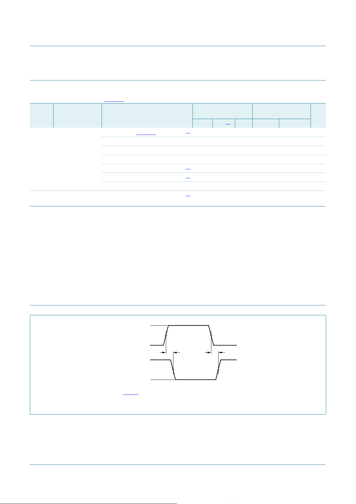
mna344
t
PHL
t
PLH
V
M
V
M
V
M
V
M
nA input
nY output
GND
V
I
V
OH
V
OL
11. Dynamic characteristics
74LV14
Hex inverting Schmitt trigger
Table 7. Dynamic characteristics
GND = 0 V; For test circuit see Figure 7.
Symbol Parameter Conditions T
Min Typ
t
pd
propagation delay nA to nY; see Figure 6
[2]
VCC = 1.2 V - 80 - - - ns
= 2.0 V - 27 37 - 48 ns
V
CC
= 2.7 V - 20 28 - 35 ns
V
CC
= 3.0 V to 3.6 V; CL=15pF
V
CC
= 3.0 V to 3.6 V
V
CC
= 4.5 V to 5.5 V - - 18 - 23 ns
V
CC
C
PD
power dissipation
capacitance
[1] All typical values are measured at T
[2] t
is the same as t
pd
PLH
CL=50pF; fi = 1 MHz;
VI=GNDtoV
amb
and t
PHL
.
CC
=25C.
[3] Typical values are measured at nominal supply voltage (V
[4] C
is used to determine the dynamic power dissipation (PDin W).
PD
P
D=CPD
= input frequency in MHz, fo= output frequency in MHz
f
i
= output load capacitance in pF
C
L
= supply voltage in V
V
CC
2
V
fi N+(CL V
CC
2
fo) where:
CC
N = number of inputs switching
2
V
(C
L
fo) = sum of the outputs.
CC
= 3.3 V).
CC
[3]
[3]
[4]
= 40 C
amb
to +85 C
[1]
Max Min Max
T
= 40 C
amb
to +125 C
Unit
-13- - -ns
- 15 22 - 28 ns
-15- - -pF
12. Waveforms
Measurement points are given in Table 8.
and VOH are typical voltage output levels that occur with the output load.
V
OL
Fig 6. The input (nA) to output (nY) propagation de la ys
74LV14 All information provided in this document is subject to legal disclaimers. © NXP B.V. 2011. All rights reserved.
Product data sheet Rev. 6 — 12 December 2011 6 of 19
 Loading...