

Page 1

INTEGRATED CIRCUITS
DATA SH EET
74HC4066; 74HCT4066
Quad bilateral switches
Product specification
Supersedes data of 1998 Nov 10
2003 Jun 17
Page 2

Philips Semiconductors Product specification
Quad bilateral switches 74HC4066; 74HCT4066
FEATURES
• Very low ON-resistance:
–50Ω(typical) at VCC= 4.5 V
–45Ω(typical) at VCC= 6.0 V
–35Ω(typical) at VCC= 9.0 V.
• Complies with JEDEC standard no. 8-1A
• ESD protection:
HBM EIA/JESD22-A114-A exceeds 2000 V
MM EIA/JESD22-A115-A exceeds 200 V.
• Specified from −40 to +85 °C and −40 to +125 °C.
QUICK REFERENCE DATA
GND = 0 V; T
=25°C; tr=tf= 6 ns.
amb
SYMBOL PARAMETER CONDITIONS
t
PZH/tPZL
t
PHZ/tPLZ
C
I
C
PD
turn-on time nE to V
turn-off time nE to V
os
os
input capacitance 3.5 3.5 pF
power dissipation
CL= 15 pF; RL=1kΩ; VCC=5V1112ns
CL= 15 pF; RL=1kΩ; VCC=5V1316ns
notes 1 and 2 11 12 pF
capacitance per switch
C
S
maximum switch
capacitance
GENERAL DESCRIPTION
The 74HC4066 and 74HCT4066 are high-speed Si-gate
CMOS devices and are pin compatible with the
HEF4066B. Theyare specified in compliance with JEDEC
standard no. 7A.
The 74HC4066 and 74HCT4066 have four independent
analog switches. Each switch has two input/output pins
(pins nY or nZ) and an active HIGH enable input pin
(pin nE).Whenpin nE = LOW the belonging analogswitch
is turned off.
The 74HC4066/74HCT4066 is pin compatible with the
74HC4016/74HCT4066 but exhibits a much lower
on-resistance. In addition, the on-resistance is relatively
constant over the full input signal range.
TYPICAL
UNIT
74HC4066 74HCT4066
88pF
Notes
1. C
is used to determine the dynamic power dissipation (PDin µW).
PD
PD=CPD× V
2
× fi× N+Σ[(CL+CS)×V
CC
2
× fo] where:
CC
fi= input frequency in MHz;
fo= output frequency in MHz;
CL= output load capacitance in pF;
CS= maximum switch capacitance in pF;
VCC= supply voltage in Volts;
N = total load switching outputs;
Σ[(CL+CS)×V
2
× fo] = sum of the outputs.
CC
2. For 74HC4066 the condition is VI= GND to VCC.
For 74HCT4066 the condition is VI= GND to VCC− 1.5 V.
2003 Jun 17 2
Page 3
Philips Semiconductors Product specification
Quad bilateral switches 74HC4066; 74HCT4066
FUNCTION TABLE
See note 1.
INPUT nE SWITCH
L off
Hon
Note
1. H = HIGH voltage level.
L = LOW voltage level.
ORDERING INFORMATION
TYPE NUMBER
PACKAGE
TEMPERATURE RANGE PINS PACKAGE MATERIAL CODE
74HC4066N −40 to 125 °C 14 DIP14 plastic SOT27-1
74HCT4066N −40 to 125 °C 14 DIP14 plastic SOT27-1
74HC4066D −40 to 125 °C 14 SO14 plastic SOT108-1
74HCT4066D −40 to 125 °C 14 SO14 plastic SOT108-1
74HC4066DB −40 to 125 °C 14 SSOP14 plastic SOT337-1
74HCT4066DB −40 to 125 °C 14 SSOP14 plastic SOT337-1
74HC4066PW −40 to 125 °C 14 TSSOP14 plastic SOT402-1
74HCT4066PW −40 to 125 °C 14 TSSOP14 plastic SOT402-1
74HC4066BQ −40 to 125 °C 14 DHVQFN14 plastic SOT762-1
74HCT4066BQ −40 to 125 °C 14 DHVQFN14 plastic SOT762-1
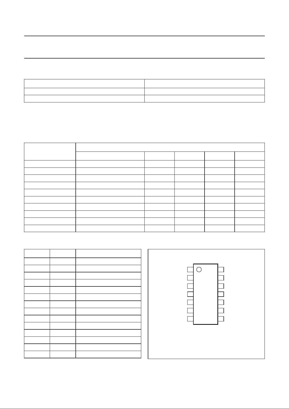
PINNING
PIN SYMBOL DESCRIPTION
1 1Y independent input/output
2 1Z independent input/output
3 2Z independent input/output
4 2Y independent input/output
handbook, halfpage
1Y
1Z
2Z
1
2
3
14
V
CC
13
1E
12
4E
5 2E enable input (active HIGH)
6 3E enable input (active HIGH)
7 GND ground (0 V)
8 3Y independent input/output
9 3Z independent input/output
10 4Z independent input/output
2Y
2E
3E
GND
4
4066
5
6
7
MGR253
11
4Y
10
4Z
9
3Z
8
3Y
11 4Y independent input/output
12 4E enable input (active HIGH)
13 1E enable input (active HIGH)
14 V
CC
supply voltage
Fig.1 Pin configuration DIP14, SO14 and
(T)SSOP14.
2003 Jun 17 3
Page 4
Philips Semiconductors Product specification
Quad bilateral switches 74HC4066; 74HCT4066
handbook, halfpage
2
1Z
3
2Z
4
2Y
5
2E
6
3E
Top view
(1) The die substrate is attached to this pad using conductive die
attach material. It can not be used as a supply pin or input.
V
1Y
CC
114
(1)
GND
8
7
GND 3Y
13
12
11
10
9
MBL891
1E
4E
4Y
4Z
3Z
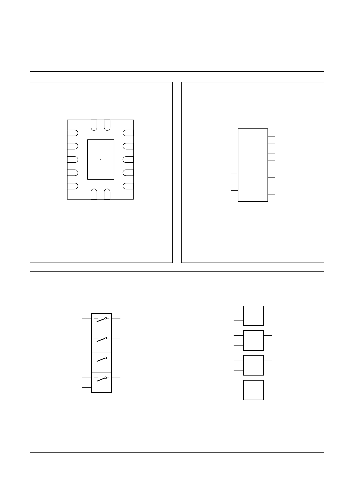
Fig.2 Pin configuration DHVQFN14.
handbook, halfpage
1E
13
52E
63E
12 4E
MGR254
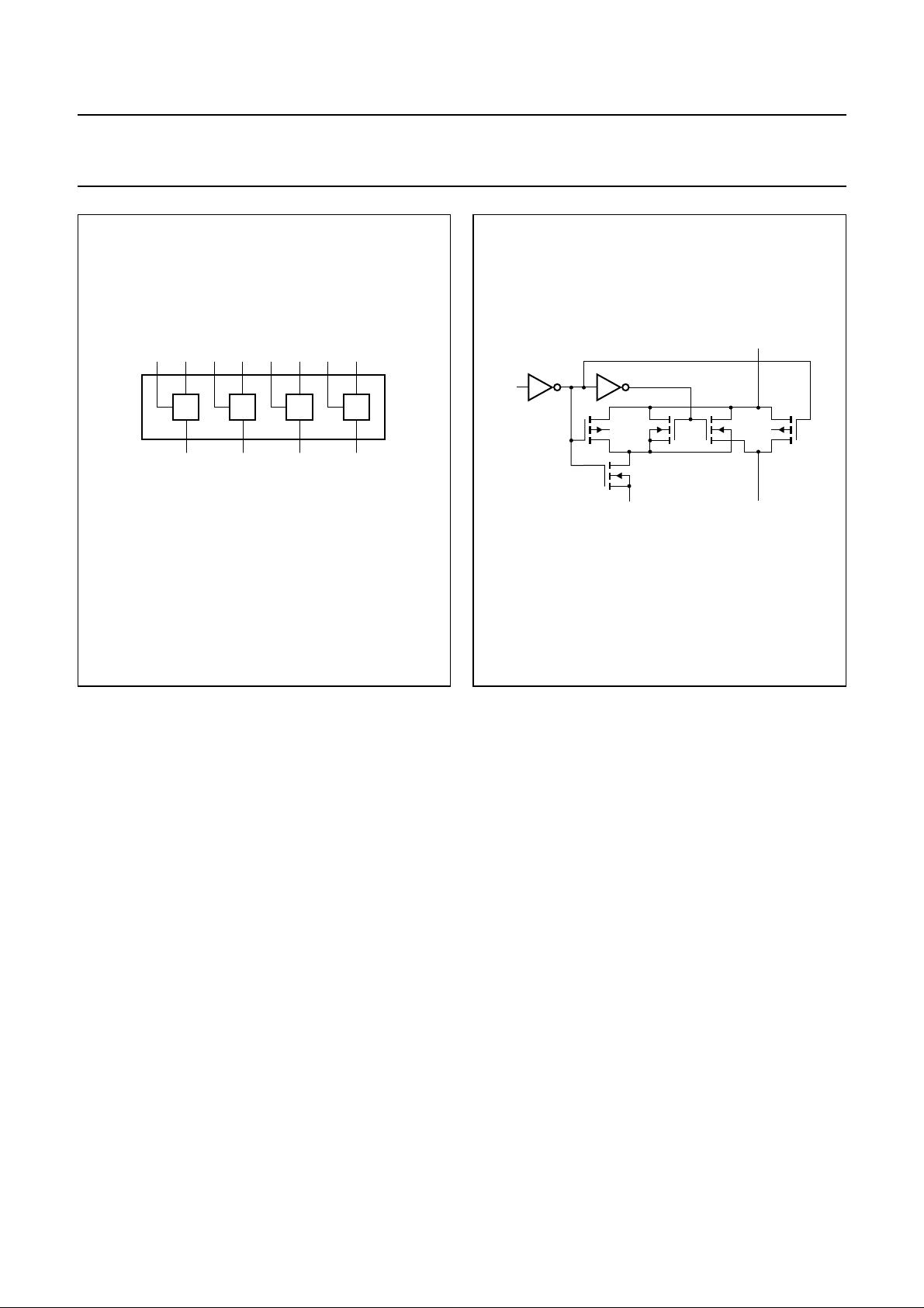
Fig.3 Logic symbol.
11Y
21Z
42Y
32Z
83Y
93Z
114Y
104Z
handbook, halfpage
1
13 #
4
5#
8
6#
11
12 #
MGR255
2
3
9
10
Fig.4 IEC logic symbol.
2003 Jun 17 4
handbook, halfpage
1
11
13 #
X1
4
11
5#
X1
8
11
6#
X1
11
11
12 #
X1
2
3
9
10
MGR256
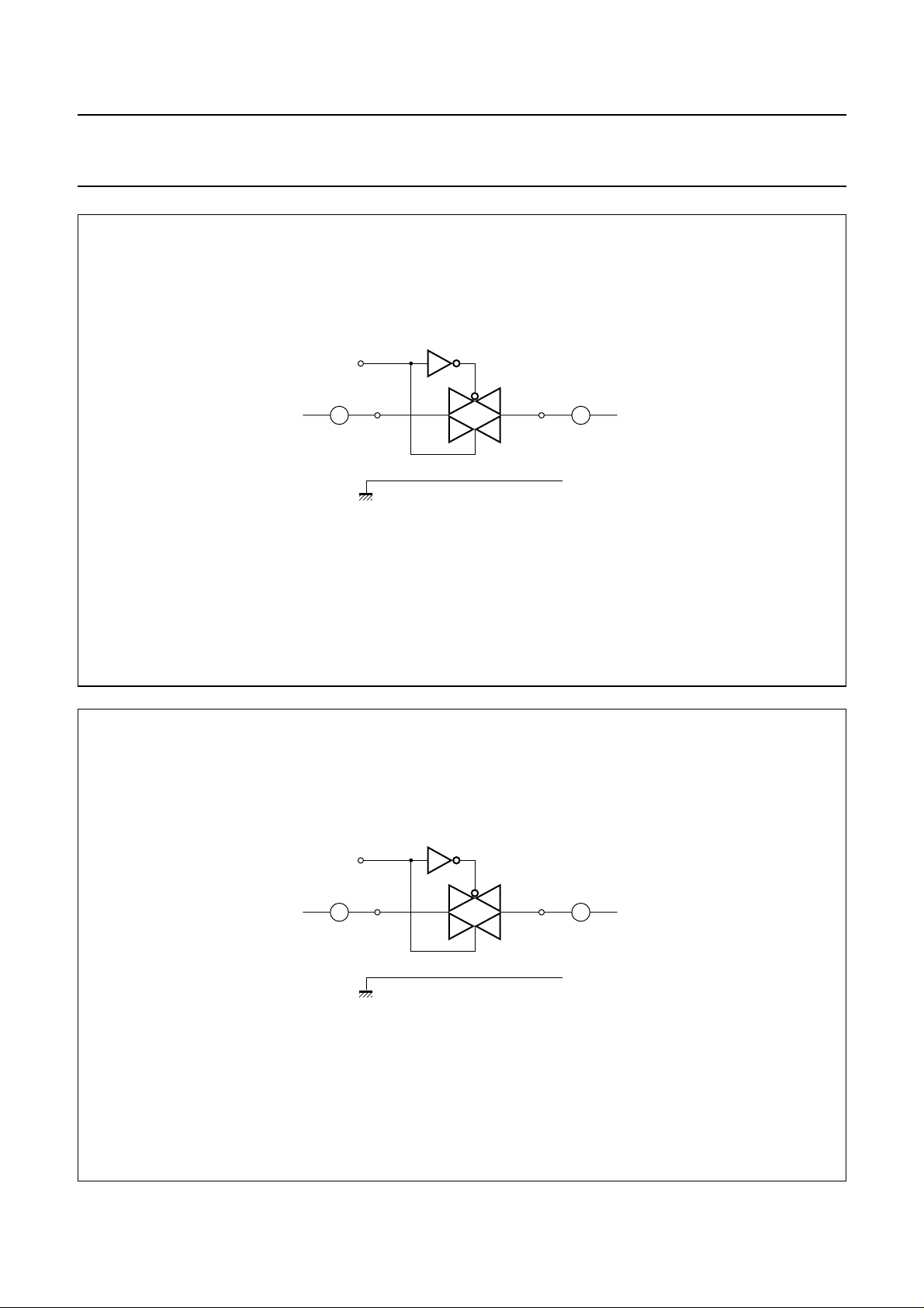
Page 5
Philips Semiconductors Product specification
Quad bilateral switches 74HC4066; 74HCT4066
handbook, halfpage
6
4
5
1
13
1E
1Y
1Z
2
2E
2Y
3E
2Z
3
Fig.5 Functional diagram.
8
3Y
3Z
9
12
4E
11
4Y
4Z
10
MGR257
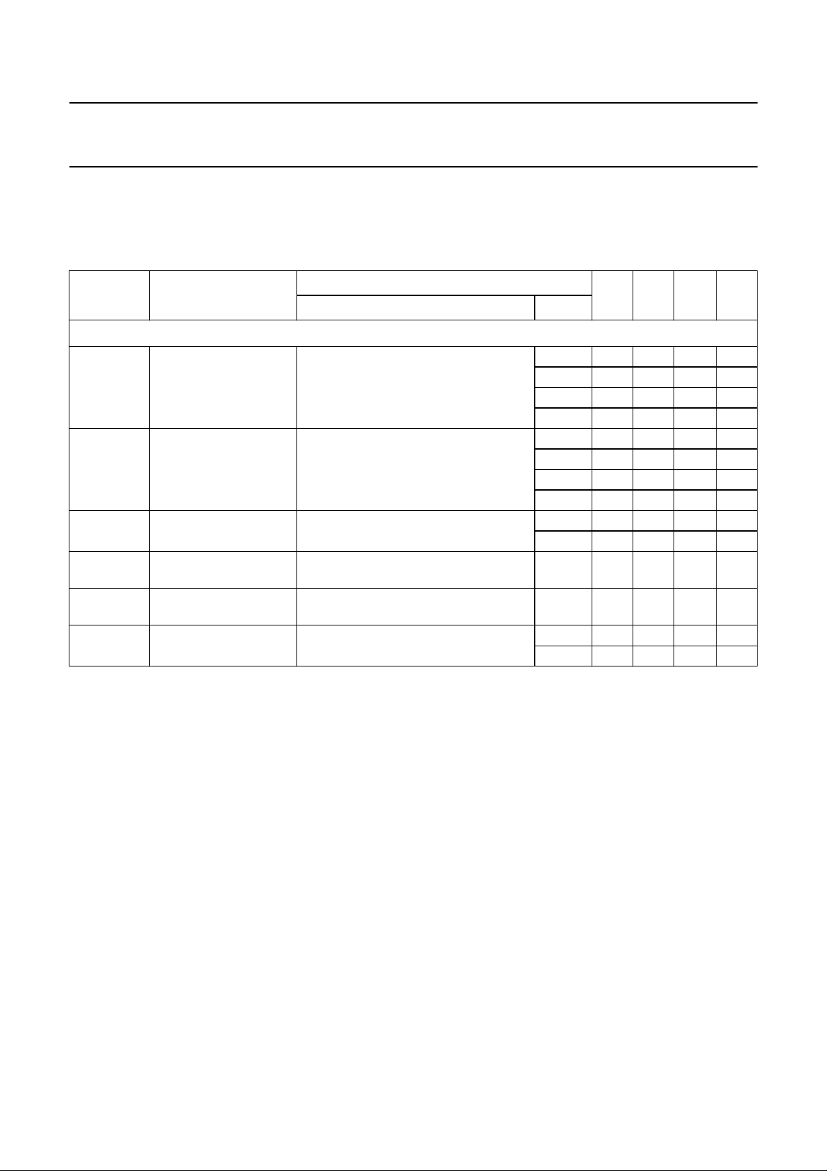
handbook, halfpage
nE
Fig.6 Schematic diagram (one switch).
V
GND
CC
nY
V
CC
nZ
MGR258
2003 Jun 17 5
Page 6
Philips Semiconductors Product specification
Quad bilateral switches 74HC4066; 74HCT4066
RECOMMENDED OPERATING CONDITIONS
SYMBOL PARAMETER CONDITIONS
UNIT
MIN. TYP. MAX. MIN. TYP. MAX.
74HC4066 74HCT4066
V
CC
V
I
V
S
T
amb
supply voltage 2.0 5.0 10.0 4.5 5.0 5.5 V
input voltage GND − V
switch voltage GND − V
operating ambient
temperature
see DC and AC
characteristics
−40 +25 +85 −40 +25 +85 °C
−40 − +125 −40 − +125 °C
GND − V
CC
GND − V
CC
CC
CC
V
V
per device
t
r,tf
input rise and fall times VCC= 2.0 V − 6.0 1000 − 6.0 500 ns
= 4.5 V −−500 −−−ns
V
CC
V
= 6.0 V −−400 −−−ns
CC
V
= 10.0 V −−250 −−−ns
CC
LIMITING VALUES
In accordance with the Absolute Maximum Rating System (IEC 60134); voltages are referenced to GND (ground = 0 V).
SYMBOL PARAMETER CONDITIONS MIN. MAX. UNIT
V
CC
I
IK
I
SK
I
S
I
, I
CC
T
stg
P
tot
P
S
supply voltage −0.5 +11.0 V
input diode current VI< −0.5 Vor VI>VCC+ 0.5 V −±20 mA
switch diode current VS< −0.5 Vor VS>VCC+ 0.5 V −±20 mA
switch current −0.5V<VO<VCC+ 0.5 V; note 1 −±25 mA
GNDVCC
or GND current −±50 mA
storage temperature −65 +150 °C
power dissipation T
= −40 to +125 °C; note 2 − 500 mW
amb
power dissipation per switch − 100 mW
Notes
1. To avoid drawing V
current out of pin nZ, when switch current flows in pin nY, the voltage drop across the
CC
bidirectional switch must not exceed 0.4 V. If the switch current flows into pin nZ, no VCCcurrent will flow out of
pin nY. In this case there is no limit for the voltage drop across the switch, but the voltages at pins nY and nZ may
not exceed VCCor GND.
2. For DIP14 packages: above 70 °C derate linearly with 12 mW/K.
For SO14 packages: above 70 °C derate linearly with 8 mW/K.
For SSOP14 and TSSOP16 packages: above 60 °C derate linearly with 5.5 mW/K.
For DHVQFN14 packages: above 60 °C derate linearly with 4.5 mW/K.
2003 Jun 17 6
Page 7
Philips Semiconductors Product specification
Quad bilateral switches 74HC4066; 74HCT4066
DC CHARACTERISTICS
Family 74HC4066
Voltages are referenced to GND (ground = 0 V); Visis the input voltage at pins nY or nZ, whichever is assigned as an
input; V
is the output voltage at pins nY or nZ, whichever is assigned as an output.
os
SYMBOL PARAMETER
T
= −40 to +85 °C; note 1
amb
V
IH
HIGH-level input
voltage
V
IL
I
LI
I
S(OFF)
LOW-level input voltage 2.0 − 0.8 0.50 V
input leakage current VI=VCCor GND 6.0 −−±1.0 µA
analog switch current
OFF-state
I
S(ON)
analog switch current
ON-state
I
CC
quiescent supply
current
TEST CONDITIONS
OTHER V
per channel; VI=VIHor VIL;
VS=VCC− GND; see Fig.7
VI=VIHor VIL; VS=VCC− GND;
see Fig.8
VI=VCCor GND; Vis= GND or VCC;
Vos=VCCor GND
MIN. TYP. MAX. UNIT
(V)
CC
2.0 1.5 1.2 − V
4.5 3.15 2.4 − V
6.0 4.2 3.2 − V
9.0 6.3 4.7 − V
4.5 − 2.1 1.35 V
6.0 − 2.8 1.80 V
9.0 − 4.3 2.70 V
10.0 −−±2.0 µA
10.0 −−±1.0 µA
10.0 −−±1.0 µA
6.0 −−20.0 µA
10.0 −−40.0 µA
2003 Jun 17 7
Page 8

Philips Semiconductors Product specification
Quad bilateral switches 74HC4066; 74HCT4066
SYMBOL PARAMETER
= −40 to +125 °C
T
amb
V
IH
HIGH-level input
voltage
V
IL
I
LI
I
S(OFF)
LOW-level input voltage 2.0 −−0.50 V
input leakage current VI=VCCor GND 6.0 −−±1.0 µA
analog switch current
OFF-state
I
S(ON)
analog switch current
ON-state
I
CC
quiescent supply
current
Note
1. All typical values are measured at T
TEST CONDITIONS
OTHER V
per channel; VI=VIHor VIL;
VS=VCC− GND; see Fig.7
VI=VIHor VIL; VS=VCC− GND; see
Fig.8
VI=VCCor GND; Vis= GND or VCC;
Vos=VCCor GND
=25°C.
amb
MIN. TYP. MAX. UNIT
(V)
CC
2.0 1.5 −−V
4.5 3.15 −−V
6.0 4.2 −−V
9.0 6.3 −−V
4.5 −−1.35 V
6.0 −−1.80 V
9.0 −−2.70 V
10.0 −−±2.0 µA
10.0 −−±1.0 µA
10.0 −−±1.0 µA
6.0 −−40.0 µA
10.0 −−80.0 µA
2003 Jun 17 8
Page 9

Philips Semiconductors Product specification
Quad bilateral switches 74HC4066; 74HCT4066
Family 74HCT4066
Voltages are referenced to GND (ground = 0 V); Visis the input voltage at pins nY or nZ, whichever is assigned as an
input; V
is the output voltage at pins nY or nZ, whichever is assigned as an output.
os
SYMBOL PARAMETER
T
= −40 to +85 °C; note 1
amb
V
IH
HIGH-level input
voltage
V
IL
I
LI
I
S(OFF)
LOW-level input voltage 4.5 to 5.5 − 1.2 0.8 V
input leakage current VI=VCCor GND 5.5 −−±1.0 µA
analog switch current
OFF-state
I
S(ON)
analog switch current
ON-state
I
CC
quiescent supply
current
∆I
CC
additional quiescent
supply current per input
T
= −40 to +125 °C
amb
V
IH
HIGH-level input
voltage
V
IL
I
LI
I
S(OFF)
LOW-level input voltage 4.5 to 5.5 −−0.8 V
input leakage current VI=VCCor GND 5.5 −−±1.0 µA
analog switch current
OFF-state
I
S(ON)
analog switch current
ON-state
I
CC
quiescent supply
current
∆I
CC
additional quiescent
supply current per input
TEST CONDITIONS
OTHER V
per channel; VI=VIHor VIL;
VS=VCC− GND; see Fig.7
VI=VIHor VIL; VS=VCC− GND; see
Fig.8
VI=VCCor GND; Vis= GND or VCC;
Vos=VCCor GND
VI=VCC− 2.1 V; other inputs at V
CC
or GND
per channel; VI=VIHor VIL;
VS=VCC− GND; see Fig.7
VI=VIHor VIL; VS=VCC− GND; see
Fig.8
VI=VCCor GND; Vis= GND or VCC;
Vos=VCCor GND
VI=VCC− 2.1 V; other inputs at V
CC
or GND
MIN. TYP. MAX. UNIT
(V)
CC
4.5 to 5.5 2.0 1.6 − V
5.5 −−±1.0 µA
5.5 −−±1.0 µA
4.5 to 5.5 −−20.0 µA
4.5 to 5.5 − 100 450 µA
4.5 to 5.5 2.0 −− V
10.0 −−±1.0 µA
10.0 −−±1.0 µA
4.5 to 5.5 −−40.0 µA
4.5 to 5.5 −−490 µA
Note
1. All typical values are measured at T
amb
=25°C.
2003 Jun 17 9
Page 10
Philips Semiconductors Product specification
Quad bilateral switches 74HC4066; 74HCT4066
handbook, full pagewidth
(from enable inputs)
VI = VCC or GND
LOW
nY
nZ
MGR260
AA
GND
Fig.7 Test circuit for measuring OFF-state current.
VO = GND or V
CC
handbook, full pagewidth
VI = VCC or GND
HIGH
(from enable inputs)
nY
Fig.8 Test circuit for measuring ON-state current.
2003 Jun 17 10
nZ
MGR261
AA
GND
VO (open circuit)
Page 11

Philips Semiconductors Product specification
Quad bilateral switches 74HC4066; 74HCT4066
Resistance RON for 74HC4066 and 74HCT4066
For 74HC4066: V
or nZ, whichever is assigned as an input; see Fig.9.
= 2.0, 4.5, 6.0 and 9.0 V; for 74HCT4066: VCC= 4.5 V; note 1; Visis the input voltage at pins nY
CC
SYMBOL PARAMETER
T
= −40 to +85 °C; note 2
amb
R
ON(peak)
ON-resistance
(peak)
R
ON(rail)
ON-resistance
(rail)
∆R
ON
maximum
variation of
ON-resistance
between any two
channels
T
= −40 to +125 °C
amb
R
ON(peak)
ON-resistance
(peak)
R
ON(rail)
ON-resistance
(rail)
TEST CONDITIONS
MIN. TYP. MAX. UNIT
OTHER I
(µA) VCC (V)
S
VI=VIHor VIL; Vis=VCCto GND 100 2.0 −−−Ω
1000 4.5 − 54 118 Ω
6.0 − 42 105 Ω
9.0 − 32 88 Ω
VI=VIHor VIL; Vis= GND 100 2.0 − 80 −Ω
1000 4.5 − 35 95 Ω
6.0 − 27 82 Ω
9.0 − 20 70 Ω
VI=VIHor VIL; Vis=V
CC
100 2.0 − 100 −Ω
1000 4.5 − 42 106 Ω
6.0 − 35 94 Ω
9.0 − 27 78 Ω
VI=VIHor VIL; Vis=VCCto GND − 2.0 −−−Ω
4.5 − 5 −Ω
6.0 − 4 −Ω
9.0 − 3 −Ω
VI=VIHor VIL; Vis=VCCto GND 100 2.0 −−−Ω
1000 4.5 −−142 Ω
6.0 −−126 Ω
9.0 −−105 Ω
VI=VIHor VIL; Vis= GND 100 2.0 −−−Ω
1000 4.5 −−115 Ω
6.0 −−100 Ω
9.0 −−85 Ω
V
I=VIH
or VIL; Vis=V
CC
100 2.0 −−−Ω
1000 4.5 −−128 Ω
6.0 −−113 Ω
9.0 −−95 Ω
Notes
1. At supply voltages approaching 2 V, the analog ON-resistance switch becomes extremely non-linear. Therefore, it is
recommended that these devices are being used to transmit digital signals only, when using these supply voltages.
2. All typical values are measured at T
amb
=25°C.
2003 Jun 17 11
Page 12

Philips Semiconductors Product specification
Quad bilateral switches 74HC4066; 74HCT4066
handbook, full pagewidth
HIGH
(from enable inputs)
nY
V
= 0 to VCC − GND
is
Fig.9 Test circuit for measuring ON-resistance (RON).
60
handbook, halfpage
R
ON
(Ω)
50
VCC = 4.5 V
MGR262
V
nZ
I
s
GND
MGR259
40
30
20
= 0 to VCC.
V
is
10
1.8 3.6 5.4 7.2
09
Fig.10 Typical ON-resistance (RON) as a function of input voltage (Vis).
2003 Jun 17 12
6 V
9 V
Vis (V)
Page 13

Philips Semiconductors Product specification
Quad bilateral switches 74HC4066; 74HCT4066
AC CHARACTERISTICS
Type 74HC4066
GND = 0 V; tr=tf= 6 ns; CL= 50 pF; Visis the input voltage at pins nY or nZ, whichever is assigned as an input; Vosis
the output voltage at pins nY or nZ, whichever is assigned as an output.
SYMBOL PARAMETER
T
= −40 to +85 °C; note 1
amb
t
PHL/tPLH
t
PZH/tPZL
t
PHZ/tPLZ
T
= −40 to +125 °C
amb
t
PHL/tPLH
t
PZH/tPZL
t
PHZ/tPLZ
propagation delay
Visto V
os
turn-on time nE to V
turn-off time nE to V
propagation delay
Visto V
os
turn-on time nE to V
turn-off time nE to V
TEST CONDITIONS
MIN. TYP. MAX. UNIT
OTHER V
CC
(V)
RL= ∞; see Fig.19 2.0 − 875ns
4.5 − 315ns
6.0 − 213ns
9.0 − 210ns
os
RL=1kΩ; see Figs 20 and 21 2.0 − 36 125 ns
4.5 − 13 25 ns
6.0 − 10 21 ns
9.0 − 816ns
os
RL=1kΩ; see Figs 20 and 21 2.0 − 44 190 ns
4.5 − 16 38 ns
6.0 − 13 33 ns
9.0 − 16 26 ns
RL= ∞; see Fig.19 2.0 −−90 ns
4.5 −−18 ns
6.0 −−15 ns
9.0 −−12 ns
os
RL=1kΩ; see Figs 20 and 21 2.0 −−150 ns
4.5 −−30 ns
6.0 −−26 ns
9.0 −−20 ns
os
RL=1kΩ; see Figs 20 and 21 2.0 −−225 ns
4.5 −−45 ns
6.0 −−38 ns
9.0 −−30 ns
Note
1. All typical values are measured at T
amb
=25°C.
2003 Jun 17 13
Page 14

Philips Semiconductors Product specification
Quad bilateral switches 74HC4066; 74HCT4066
Type 74HCT4066
GND = 0 V; tr=tf= 6 ns; CL= 50 pF; Visis the input voltage at pins nY or nZ, whichever is assigned as an input; Vosis
the output voltage at pins nY or nZ, whichever is assigned as an output.
SYMBOL PARAMETER
= −40 to +85 °C; note 1
T
amb
t
PHL/tPLH
t
PZH/tPZL
t
PHZ/tPLZ
T
= −40 to +125 °C
amb
t
PHL/tPLH
t
PZH/tPZL
t
PHZ/tPLZ
propagation delay
Visto V
os
turn-on time nE to V
turn-off time nE to V
propagation delay
Visto V
os
turn-on time nE to V
turn-off time nE to V
OTHER V
CC
RL= ∞; see Fig.19 4.5 − 315ns
os
os
RL=1kΩ; see Figs 20 and 21 4.5 − 12 30 ns
RL=1kΩ; see Figs 20 and 21 4.5 − 20 44 ns
RL= ∞; see Fig.19 4.5 −−18 ns
os
os
RL=1kΩ; see Figs 20 and 21 4.5 −−36 ns
RL=1kΩ; see Figs 20 and 21 4.5 −−53 ns
MIN. TYP. MAX. UNIT
(V)
Note
TEST CONDITIONS
1. All typical values are measured at T
amb
=25°C.
74HC4066 and 74HCT4066
At recommended conditions and typical values; GND = 0 V; tr=tf= 6 ns; Visis the input voltage at pins nY or nZ,
whichever is assigned as an input; V
is the output voltage at pins nY or nZ, whichever is assigned as an output.
os
CONDITIONS
SYMBOL PARAMETER
d
sin
α
OFF(feedthr)
sine wave distortion f = 1 kHz; RL=10kΩ; CL=50pF;
switch OFF signal
feed-through
α
ct(s)
crosstalk between any two
switches
V
ct(p-p)
crosstalk voltage between
any input to any switch
(peak-to-peak value)
OTHER V
see Fig.17
f = 10 kHz; R
=10kΩ;CL=50pF;
L
see Fig.17
RL= 600 Ω; CL= 50 pF; f = 1 MHz;
see Figs 11 and 18
RL= 600 Ω; CL= 50 pF; f = 1 MHz;
see Fig.13
RL= 600 Ω; CL= 50 pF; f = 1 MHz;
see Fig.15 (nE, square wave
between VCC and GND,
(V) VCC (V)
is(p-p)
4.0 4.5 0.04 %
8.0 9.0 0.02 %
4.0 4.5 0.12 %
8.0 9.0 0.06 %
note 1 4.5 −50 dB
9.0 −50 dB
note 1 4.5 −60 dB
9.0 −60 dB
− 4.5 110 mV
9.0 220 mV
TYP. UNIT
tr=tf= 6 ns)
f
max
C
S
minimum frequency
response (−3 dB)
maximum switch
RL=50Ω;CL= 10 pF; see Figs 12
and 16
note 2 4.5 180 MHz
9.0 200 MHz
−−8pF
capacitance
Notes
1. Adjust input voltage V
is 0 dBM level (0 dBM = 1 mW into 600 Ω).
is
2. Adjust input voltage Visis 0 dBM level at Vosfor 1 MHz (0 dBM = 1 mW into 50 Ω).
2003 Jun 17 14
Page 15

Philips Semiconductors Product specification
Quad bilateral switches 74HC4066; 74HCT4066
handbook, full pagewidth
0
(dB)
−20
−40
−60
−80
−100
10 10
2
Test conditions: VCC= 4.5 V; GND = 0 V; RL=50Ω; R
Fig.11 Typical switch OFF signal feed-through as a function of frequency.
source
3
10
=1kΩ.
MGR263
4
10
5
10
f (kHz)
6
10
handbook, full pagewidth
5
(dB)
0
−5
10 10
2
Test conditions: VCC= 4.5 V; GND = 0 V; RL=50Ω; R
source
3
10
=1kΩ.
4
10
Fig.12 Typical frequency response.
MGR264
5
10
f (kHz)
6
10
2003 Jun 17 15
Page 16

Philips Semiconductors Product specification
Quad bilateral switches 74HC4066; 74HCT4066
handbook, full pagewidth
Fig.13 Test circuit for measuring crosstalk between any two switches; channels ON condition.
V
I
0.1 µF
V
CC
2R
L
R
L
channel
ON
2R
nZ/nYnY/nZ
C
L
L
GND
MGR265
handbook, full pagewidth
2R
V
CC
2R
L
L
channel
OFF
V
CC
Fig.14 Test circuit for measuring crosstalk between any two switches; channels OFF condition.
2003 Jun 17 16
2R
L
2R
L
CLdB
nZ/nYnY/nZ
MGR266
V
os
GND
Page 17

Philips Semiconductors Product specification
Quad bilateral switches 74HC4066; 74HCT4066
The crosstalk is defined as follows
(oscilloscope output).
page
V
CC
GND
2R
V
CC
2R
L
C
L
L
handbook, full pagewidth
V
ct(p-p)
MGR267
V
CC
2R
L
2R
nE
D.U.T.
L
Fig.15 Test circuit for measuring crosstalk between control and any switch.
nZ/nYnY/nZ
oscilloscope
MGR268
V
os
GND
handbook, full pagewidth
0.1 µF
V
sine-wave
Adjust input voltage to obtain 0 dB at Vos when fi= 1 MHz. After set-up, the frequency of fi is increased to obtain a reading of -3 dB at Vos.
is
channel
ON
V
CC
2R
L
2R
CLdB
L
nZ/nYnY/nZ
MGR269
V
os
GND
Fig.16 Test circuit for measuring minimum frequency response.
2003 Jun 17 17
Page 18

Philips Semiconductors Product specification
Quad bilateral switches 74HC4066; 74HCT4066
handbook, full pagewidth
fi = 1 kHz
sine-wave
V
CC
2R
10 µF
V
is
channel
ON
L
DISTORTION
2R
C
L
L
METER
Fig.17 Test circuit for measuring sine wave distortion.
nZ/nYnY/nZ
V
os
GND
MGR270
handbook, full pagewidth
V
0.1 µF
is
channel
OFF
V
CC
Fig.18 Test circuit for measuring switch OFF signal feed-through.
2003 Jun 17 18
2R
L
2R
CLdB
L
nZ/nYnY/nZ
MGR271
V
os
GND
Page 19

Philips Semiconductors Product specification
Quad bilateral switches 74HC4066; 74HCT4066
AC WAVEFORMS
handbook, full pagewidth
t
r
90%
V
is
V
os
10%
50%
50%
t
PLH
t
f
V
CC
GND
t
PHL
MGR272
Fig.19 Waveforms showing the input (Vis) to output (Vos) propagation delays.
t
f
90 %
nE input
LOW - to - OFF
OFF - to - LOW
HIGH - to - OFF
OFF - to - HIGH
MGA846
74HC4066: VM= 50%; VI= GND to VCC.
74HCT4066: V
= 1.3 V; VI= GND to 3 V.
M
output
output
V
M
10 %
t
PLZ
10 %
t
PHZ
outputs
enabled
Fig.20 Waveforms showing the turn-on and turn-off times.
2003 Jun 17 19
90 %
outputs
disabled
t
r
t
PZL
50 %
t
PZH
50 %
outputs
enabled
Page 20

Philips Semiconductors Product specification
Quad bilateral switches 74HC4066; 74HCT4066
TEST CIRCUIT AND WAVEFORMS
V
handbook, full pagewidth
PULSE
GENERATOR
V
CC
is
V
I
D.U.T.
R
T
V
O
R
L
C
L
switch
V
CC
open
MGR273
GND
TEST SWITCH V
t
PZH
t
PZL
t
PHZ
t
PLZ
GND V
V
CC
GND V
V
CC
is
CC
GND
CC
GND
other open pulse
Definitions for test circuit:
RL= Load resistance.
CL= Load capacitance including jig and probe capacitance.
RT= Termination resistance should be equal to the output impedance ZOof the pulse generator.
Fig.21 Test circuit for measuring AC performance.
handbook, full pagewidth
negative
input pulse
positive
input pulse
90%
10%
V
V
M
10%
90%
M
t
THL
t
TLH
t
W
(tf)t
(tr)t
t
W
tf= 6 ns; when measuring f
constraint to t
TLH
THL
and tf with 50% duty factor.
r
amplitude
0 V
(tr)
(tf)
amplitude
0 V
MGR274
, there is no
max
tr and t
FAMILY AMPLITUDE V
M
f
; PULSE
max
WIDTH
74HC4066 V
CC
50% <2ns 6ns
74HCT4066 3.0 V 1.3 V <2ns 6ns
Fig.22 Input pulse definitions.
2003 Jun 17 20
f
OTHER
Page 21

Philips Semiconductors Product specification
Quad bilateral switches 74HC4066; 74HCT4066
PACKAGE OUTLINES
DIP14: plastic dual in-line package; 14 leads (300 mil)
D
seating plane
L
Z
14
pin 1 index
e
b
SOT27-1
M
E
A
2
A
A
1
w M
b
1
8
E
c
(e )
1
M
H
1
0 5 10 mm
DIMENSIONS (inch dimensions are derived from the original mm dimensions)
A
UNIT
mm
inches
Note
1. Plastic or metal protrusions of 0.25 mm (0.01 inch) maximum per side are not included.
max.
OUTLINE
VERSION
SOT27-1
A
min.
A
1 2
max.
IEC JEDEC JEITA
050G04 MO-001 SC-501-14
b
1.73
1.13
0.068
0.044
b
0.53
0.38
0.021
0.015
1
cD
0.36
0.23
0.014
0.009
REFERENCES
scale
(1) (1)
19.50
18.55
0.77
0.73
7
Ee M
6.48
6.20
0.26
0.24
2003 Jun 17 21
M
e
L
1
3.60
3.05
0.14
0.12
E
8.25
7.80
0.32
0.31
EUROPEAN
PROJECTION
10.0
8.3
0.39
0.33
H
ISSUE DATE
w
0.2542.54 7.62
0.010.1 0.3
99-12-27
03-02-13
max.
2.24.2 0.51 3.2
0.0870.17 0.02 0.13
(1)
Z
Page 22

Philips Semiconductors Product specification
Quad bilateral switches 74HC4066; 74HCT4066
SO14: plastic small outline package; 14 leads; body width 3.9 mm
D
c
y
Z
14
pin 1 index
1
e
8
A
2
7
w M
b
p
SOT108-1
E
H
E
A
1
L
detail X
A
X
v M
A
Q
(A )
L
p
A
3
θ
0 2.5 5 mm
scale
DIMENSIONS (inch dimensions are derived from the original mm dimensions)
UNIT
mm
inches
Note
1. Plastic or metal protrusions of 0.15 mm (0.006 inch) maximum per side are not included.
A
max.
1.75
0.069
OUTLINE
VERSION
SOT108-1
A
1
0.25
0.10
0.010
0.004
A2A3b
1.45
0.25
1.25
0.057
0.01
0.049
IEC JEDEC JEITA
076E06 MS-012
p
0.49
0.36
0.019
0.014
0.25
0.19
0.0100
0.0075
(1)E(1)
cD
8.75
8.55
0.35
0.34
REFERENCES
eHELLpQZywv θ
4.0
1.27
3.8
0.16
0.15
0.05
0.244
0.228
2003 Jun 17 22
6.2
5.8
1.05
0.041
1.0
0.4
0.039
0.016
0.7
0.25
0.6
0.028
0.01 0.004
0.024
EUROPEAN
PROJECTION
0.25 0.1
0.01
(1)
0.7
0.3
0.028
0.012
ISSUE DATE
99-12-27
03-02-19
o
8
o
0
Page 23

Philips Semiconductors Product specification
Quad bilateral switches 74HC4066; 74HCT4066
SSOP14: plastic shrink small outline package; 14 leads; body width 5.3 mm
D
c
y
Z
14
pin 1 index
8
A
2
A
E
H
E
1
SOT337-1
A
X
v M
A
Q
(A )
L
p
L
A
3
θ
p
7
b
p
cD
0.20
6.4
0.09
6.0
REFERENCES
MO-150
w M
0 2.5 5 mm
scale
(1)E(1)
5.4
0.65 1.25 0.2
5.2
1
e
DIMENSIONS (mm are the original dimensions)
mm
OUTLINE
VERSION
SOT337-1
A
max.
2
1
0.21
0.05
A2A3b
1.80
1.65
IEC JEDEC JEITA
0.25
0.38
0.25
UNIT A
Note
1. Plastic or metal protrusions of 0.25 mm maximum per side are not included.
2003 Jun 17 23
detail X
eHELLpQZywv θ
7.9
7.6
1.03
0.63
0.9
0.7
EUROPEAN
PROJECTION
0.13 0.1
(1)
1.4
0.9
ISSUE DATE
99-12-27
03-02-19
o
8
o
0
Page 24

Philips Semiconductors Product specification
Quad bilateral switches 74HC4066; 74HCT4066
TSSOP14: plastic thin shrink small outline package; 14 leads; body width 4.4 mm
D
c
y
Z
14
pin 1 index
8
17
w M
b
e
p
A
2
A
1
E
H
E
L
detail X
SOT402-1
A
X
v M
A
Q
(A )
3
A
θ
L
p
0 2.5 5 mm
scale
DIMENSIONS (mm are the original dimensions)
UNIT A1A2A3b
Notes
1. Plastic or metal protrusions of 0.15 mm maximum per side are not included.
2. Plastic interlead protrusions of 0.25 mm maximum per side are not included.
A
max.
0.15
mm
1.1
OUTLINE
VERSION
SOT402-1 MO-153
0.05
0.95
0.25
0.80
IEC JEDEC JEITA
p
0.30
0.19
0.2
0.1
(1)E(2) (1)
cD
5.1
4.5
4.3
0.65
4.9
REFERENCES
2003 Jun 17 24
eHELLpQZywv θ
6.6
6.2
0.75
0.50
0.4
0.3
EUROPEAN
PROJECTION
0.13 0.10.21
0.72
0.38
ISSUE DATE
99-12-27
03-02-18
o
8
o
0
Page 25

Philips Semiconductors Product specification
Quad bilateral switches 74HC4066; 74HCT4066
DHVQFN14: plastic dual in-line compatible thermal enhanced very thin quad flat package; no leads;
14 terminals; body 2.5 x 3 x 0.85 mm
A
D
B
A
A
E
1
SOT762-1
c
terminal 1
index area
terminal 1
index area
L
1
E
h
14
DIMENSIONS (mm are the original dimensions)
(1)
A
UNIT
mm
Note
1. Plastic or metal protrusions of 0.075 mm maximum per side are not included.
max.
A
0.05
0.00
b
1
0.30
0.18
e
26
13
c
0.2
e
1
b
9
D
h
0 2.5 5 mm
D
3.1
2.9
(1)
1.65
1.35
(1)
E
2.6
2.4
E
1.15
0.85
h
D
h
v
w
7
e
8
scale
0.51
detail X
C
M
ACCB
M
e
L
1
0.5
2
0.3
y
w
0.1v0.05
C
1
ye
y
0.05 0.1
1
y
X
OUTLINE
VERSION
SOT762-1 MO-241 - - -- - -
IEC JEDEC JEITA
REFERENCES
2003 Jun 17 25
EUROPEAN
PROJECTION
ISSUE DATE
02-10-17
03-01-27
Page 26

Philips Semiconductors Product specification
Quad bilateral switches 74HC4066; 74HCT4066
SOLDERING
Introduction
Thistext gives a very briefinsightto a complex technology.
A more in-depth account of soldering ICs can be found in
our
“Data Handbook IC26; Integrated Circuit Packages”
(document order number 9398 652 90011).
There is no soldering method that is ideal for all IC
packages. Wave soldering is often preferred when
through-holeandsurfacemountcomponents are mixed on
one printed-circuit board. Wave soldering can still be used
for certain surface mount ICs, but it is not suitable for fine
pitch SMDs. In these situations reflow soldering is
recommended. Driven by legislation and environmental
forces the worldwide use of lead-free solder pastes is
increasing.
Through-hole mount packages
SOLDERING BY DIPPING OR BY SOLDER WAVE
Typical dwell time of the leads in the wave ranges from
3 to 4 seconds at 250 °C or 265 °C, depending on solder
material applied, SnPb or Pb-free respectively.
Thetotalcontact time of successivesolderwavesmust not
exceed 5 seconds.
The device may be mounted up to the seating plane, but
the temperature of the plastic body must not exceed the
specified maximum storage temperature (T
printed-circuit board has been pre-heated, forced cooling
may be necessary immediately after soldering to keep the
temperature within the permissible limit.
MANUAL SOLDERING
Apply the soldering iron (24 V or less) to the lead(s) of the
package, either below the seating plane or not more than
2 mm above it. If the temperature of the soldering iron bit
is less than 300 °C it may remain in contact for up to
10 seconds. If the bit temperature is between
300 and 400 °C, contact may be up to 5 seconds.
Surface mount packages
REFLOW SOLDERING
Reflow soldering requires solder paste (a suspension of
fine solder particles, flux and binding agent) to be applied
tothe printed-circuit boardbyscreen printing, stencilling or
pressure-syringe dispensing before package placement.
Several methods exist for reflowing; for example,
convection or convection/infrared heating in a conveyor
stg(max)
). If the
type oven. Throughput times (preheating, soldering and
cooling) vary between 100 and 200 seconds depending
on heating method.
Typical reflow peak temperatures range from
215 to 270 °C depending on solder paste material. The
top-surface temperature of the packages should
preferably be kept:
• below 220 °C (SnPb process) or below 245 °C (Pb-free
process)
– for all the BGA packages
– for packages with a thickness≥ 2.5 mm
– for packages with a thickness <2.5 mm and a
volume ≥ 350 mm3 so called thick/large packages.
• below 235 °C (SnPb process) or below 260 °C (Pb-free
process) for packages with a thickness < 2.5 mm and a
volume < 350 mm3 so called small/thin packages.
Moisture sensitivity precautions, as indicated on packing,
must be respected at all times.
WAVE SOLDERING
Conventional single wave soldering is not recommended
forsurfacemount devices (SMDs) orprinted-circuitboards
with a high component density, as solder bridging and
non-wetting can present major problems.
To overcome these problems the double-wave soldering
method was specifically developed.
If wave soldering is used the following conditions must be
observed for optimal results:
• Use a double-wave soldering method comprising a
turbulent wave with high upward pressure followed by a
smooth laminar wave.
• For packages with leads on two sides and a pitch (e):
– larger than or equal to 1.27mm, the footprint
longitudinal axis is preferred to be parallel to the
transport direction of the printed-circuit board;
– smaller than 1.27mm, the footprint longitudinal axis
must be parallel to the transport direction of the
printed-circuit board.
The footprint must incorporate solder thieves at the
downstream end.
• Forpackageswith leads on foursides,thefootprint must
be placed at a 45° angle to the transport direction of the
printed-circuit board. The footprint must incorporate
solder thieves downstream and at the side corners.
2003 Jun 17 26
Page 27

Philips Semiconductors Product specification
Quad bilateral switches 74HC4066; 74HCT4066
During placement andbefore soldering, the package must
be fixed with a droplet of adhesive. The adhesive can be
applied by screen printing, pin transfer or syringe
dispensing. The package can be soldered after the
adhesive is cured.
Typical dwell time of the leads in the wave ranges from
3 to 4 seconds at 250 °C or 265 °C, depending on solder
material applied, SnPb or Pb-free respectively.
MANUAL SOLDERING
Fix the component by first soldering two
diagonally-opposite end leads. Use a low voltage (24 V or
less) soldering iron applied to the flat part of the lead.
Contact time must be limited to 10 seconds at up to
300 °C. When using a dedicated tool, all other leads can
be soldered in one operation within 2 to 5 seconds
between 270 and 320 °C.
A mildly-activated flux will eliminate the need for removal
of corrosive residues in most applications.
Suitability of IC packages for wave, reflow and dipping soldering methods
MOUNTING PACKAGE
(1)
Through-hole mount DBS, DIP, HDIP, SDIP, SIL suitable
SOLDERING METHOD
WAVE REFLOW
(3)
− suitable
(2)
Surface mount BGA, LBGA, LFBGA, SQFP, TFBGA, VFBGA not suitable suitable −
DHVQFN, HBCC, HBGA, HLQFP, HSQFP,
not suitable
(4)
suitable −
HSOP, HTQFP, HTSSOP, HVQFN, HVSON,
SMS
(5)
PLCC
LQFP, QFP, TQFP not recommended
SSOP, TSSOP, VSO, VSSOP not recommended
, SO, SOJ suitable suitable −
(5)(6)
suitable −
(7)
suitable −
DIPPING
Notes
1. Formore detailed information onthe BGA packages refertothe
“(LF)BGAApplication Note
”(AN01026); order a copy
from your Philips Semiconductors sales office.
2. All surface mount (SMD) packages are moisture sensitive. Depending upon the moisture content, the maximum
temperature (with respect to time) and body size of the package, there is a risk that internal or external package
cracks may occur due to vaporization of the moisture in them (the so called popcorn effect). For details, refer to the
Drypack information in the
“Data Handbook IC26; Integrated Circuit Packages; Section: Packing Methods”
.
3. For SDIP packages, the longitudinal axis must be parallel to the transport direction of the printed-circuit board.
4. These packages are not suitable for wave soldering. On versions with the heatsink on the bottom side, the solder
cannot penetrate between the printed-circuit board and the heatsink. On versions with the heatsink on the top side,
the solder might be deposited on the heatsink surface.
5. If wave soldering is considered, then the package must be placed at a 45° angle to the solder wave direction.
The package footprint must incorporate solder thieves downstream and at the side corners.
6. Wave soldering is suitable for LQFP, QFP and TQFP packages with a pitch (e) larger than 0.8 mm; it is definitely not
suitable for packages with a pitch (e) equal to or smaller than 0.65 mm.
7. Wave soldering is suitable for SSOP, TSSOP, VSO and VSSOP packages with a pitch (e) equal to or larger than
0.65 mm; it is definitely not suitable for packages with a pitch (e) equal to or smaller than 0.5 mm.
2003 Jun 17 27
Page 28

Philips Semiconductors Product specification
Quad bilateral switches 74HC4066; 74HCT4066
DATA SHEET STATUS
LEVEL
DATA SHEET
STATUS
(1)
PRODUCT
STATUS
(2)(3)
DEFINITION
I Objective data Development This data sheet contains data from the objective specification for product
development. Philips Semiconductors reserves the right to change the
specification in any manner without notice.
II Preliminary data Qualification This data sheet contains data from the preliminary specification.
Supplementary data will be published at a later date. Philips
Semiconductors reserves the right to change the specification without
notice, in order to improve the design and supply the best possible
product.
III Product data Production This data sheet contains data from the product specification. Philips
Semiconductors reserves the right to make changes at any time in order
to improve the design, manufacturing and supply. Relevant changes will
be communicated via a Customer Product/Process Change Notification
(CPCN).
Notes
1. Please consult the most recently issued data sheet before initiating or completing a design.
2. The product status of the device(s) described in this data sheet may have changed since this data sheet was
published. The latest information is available on the Internet at URL http://www.semiconductors.philips.com.
3. For data sheets describing multiple type numbers, the highest-level product statusdetermines thedata sheetstatus.
DEFINITIONS
DISCLAIMERS
Short-form specification The data in a short-form
specification is extracted from a full data sheet with the
same type number and title. For detailed information see
the relevant data sheet or data handbook.
Limiting values definition Limiting values given are in
accordance with the Absolute Maximum Rating System
(IEC 60134). Stress above one or more of the limiting
values may cause permanent damage to the device.
These are stress ratings only and operation of the device
atthese or at anyotherconditions above those giveninthe
Characteristics sections of the specification is not implied.
Exposure to limiting values for extended periods may
affect device reliability.
Application information Applications that are
described herein for any of these products are for
illustrative purposes only. Philips Semiconductors make
norepresentationor warranty that such applications willbe
suitable for the specified use without further testing or
modification.
Life support applications These products are not
designed for use in life support appliances, devices, or
systems where malfunction of these products can
reasonably be expectedto result inpersonal injury. Philips
Semiconductorscustomersusingor selling these products
for use in such applications do so at their own risk and
agree to fully indemnify Philips Semiconductors for any
damages resulting from such application.
Right to make changes Philips Semiconductors
reserves the right to make changes in the products including circuits, standard cells, and/or software described or contained herein in order to improve design
and/or performance. Whenthe productis in full production
(status ‘Production’), relevant changes will be
communicated via a Customer Product/Process Change
Notification (CPCN). Philips Semiconductors assumes no
responsibility or liability for the use of any of these
products, conveys no licence or title under any patent,
copyright, or mask work right to these products, and
makes no representations or warranties that these
products are free from patent, copyright, or mask work
right infringement, unless otherwise specified.
2003 Jun 17 28
Page 29

Philips Semiconductors Product specification
Quad bilateral switches 74HC4066; 74HCT4066
NOTES
2003 Jun 17 29
Page 30

Philips Semiconductors Product specification
Quad bilateral switches 74HC4066; 74HCT4066
NOTES
2003 Jun 17 30
Page 31

Philips Semiconductors Product specification
Quad bilateral switches 74HC4066; 74HCT4066
NOTES
2003 Jun 17 31
Page 32

Philips Semiconductors – a w orldwide compan y
Contact information
For additional information please visit http://www.semiconductors.philips.com. Fax: +31 40 27 24825
For sales offices addresses send e-mail to: sales.addresses@www.semiconductors.philips.com.
© Koninklijke Philips Electronics N.V. 2003
All rights are reserved. Reproduction in whole or in part is prohibited without the prior written consent of the copyright owner.
The information presented in this document does not form part of any quotation or contract, is believed to be accurate and reliable and may be changed
without notice. No liability will be accepted by the publisher for any consequence of its use. Publication thereof does not convey nor imply any license
under patent- or other industrial or intellectual property rights.
Printed in The Netherlands 613508/04/pp32 Date of release:2003 Jun 17 Document order number: 9397 750 11264
SCA75
 Loading...