

NSC LMC6492MWC, LMC6492BEN, LMC6492BEM, LMC6492AEMX, LMC6492AEM Datasheet
...
LMC6492 Dual/LMC6494 Quad
CMOS Rail-to-Rail Input and Output Operational
Amplifier
General Description
The LMC6492/LMC6494 amplifiers were specifically developed for single supply applications that operate from −40˚C
to +125˚C. Thisfeatureiswell-suitedfor automotive systems
because of the wide temperature range. A unique design topology enables the LMC6492/LMC6494 common-mode voltage range to accommodate input signals beyond the rails.
This eliminates non-linear output errors due to input signals
exceeding a traditionally limited common-mode voltage
range. The LMC6492/LMC6494 signal range has a high
CMRR of 82 dB for excellent accuracy in non-inverting circuit
configurations.
The LMC6492/LMC6494 rail-to-rail input is complemented
by rail-to-rail output swing. This assures maximum dynamic
signal range which is particularly important in 5V systems.
Ultra-low input current of 150 fA and 120 dB open loop gain
provide high accuracy and direct interfacing with high impedance sources.
Features
(Typical unless otherwise noted)
n Rail-to-Rail input common-mode voltage range,
guaranteed over temperature
n Rail-to-Rail output swing within 20 mV of supply rail,
100 kΩ load
n Operates from 5V to 15V supply
n Excellent CMRR and PSRR 82 dB
n Ultra low input current 150 fA
n High voltage gain (R
L
=
100 kΩ) 120 dB
n Low supply current (
@
V
S
=
5V) 500 µA/Amplifier
n Low offset voltage drift 1.0 µV/˚C
Applications
n Automotive transducer amplifier
n Pressure sensor
n Oxygen sensor
n Temperature sensor
n Speed sensor
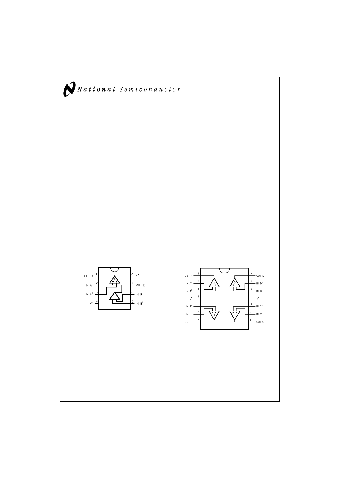
Connection Diagrams
8-Pin DIP/SO
DS012049-1
Top View
14-Pin DIP/SO
DS012049-2
Top View
October 1994
LMC6492 Dual/LMC6494 Quad CMOS Rail-to-Rail Input and Output Operational Amplifier
© 1999 National Semiconductor Corporation DS012049 www.national.com
Ordering Information
Package
Temperature Range Transport
Media
NSC
Drawing
Extended −40˚C to +125˚C
8-Pin Small Outline LMC6492AEM Rails M08A
LMC6492BEM
LMC6492AEMX Tape and Reel
LMC6492BEMX
8-Pin Molded DIP LMC6492AEN Rails N08A
LMC6492BEN
14-Pin Small Outline LMC6494AEM Rails M14A
LMC6494BEM
LMC6494AEMX Tape and Reel
LMC6494BEMX
14-Pin Molded DIP LMC6494AEN Rails N14A
LMC6494BEN
www.national.com 2
Absolute Maximum Ratings (Note 1)
If Military/Aerospace specified devices are required,
please contact the National Semiconductor Sales Office/
Distributors for availability and specifications.
ESD Tolerance (Note 2) 2000V
Differential Input Voltage
±
Supply Voltage
Voltage at Input/Output Pin (V
+
) + 0.3V, (V−) − 0.3V
Supply Voltage (V
+−V−
) 16V
Current at Input Pin
±
5mA
Current at Output Pin (Note 3)
±
30 mA
Current at Power Supply Pin 40 mA
Lead Temp. (Soldering, 10 sec.) 260˚C
Storage Temperature Range −65˚C to +150˚C
Junction Temperature (Note 4) 150˚C
Operating Conditions (Note 1)
Supply Voltage 2.5V ≤ V
+
≤ 15.5V
Junction Temperature Range
LMC6492AE, LMC6492BE −40˚C ≤ T
J
≤ +125˚C
LMC6494AE, LMC6494BE −40˚C ≤ T
J
≤ +125˚C
Thermal Resistance (θ
JA
)
N Package, 8-Pin Molded DIP 108˚C/W
M Package, 8-Pin Surface Mount 171˚C/W
N Package, 14-Pin Molded DIP 78˚C/W
M Package, 14-Pin Surface Mount 118˚C/W
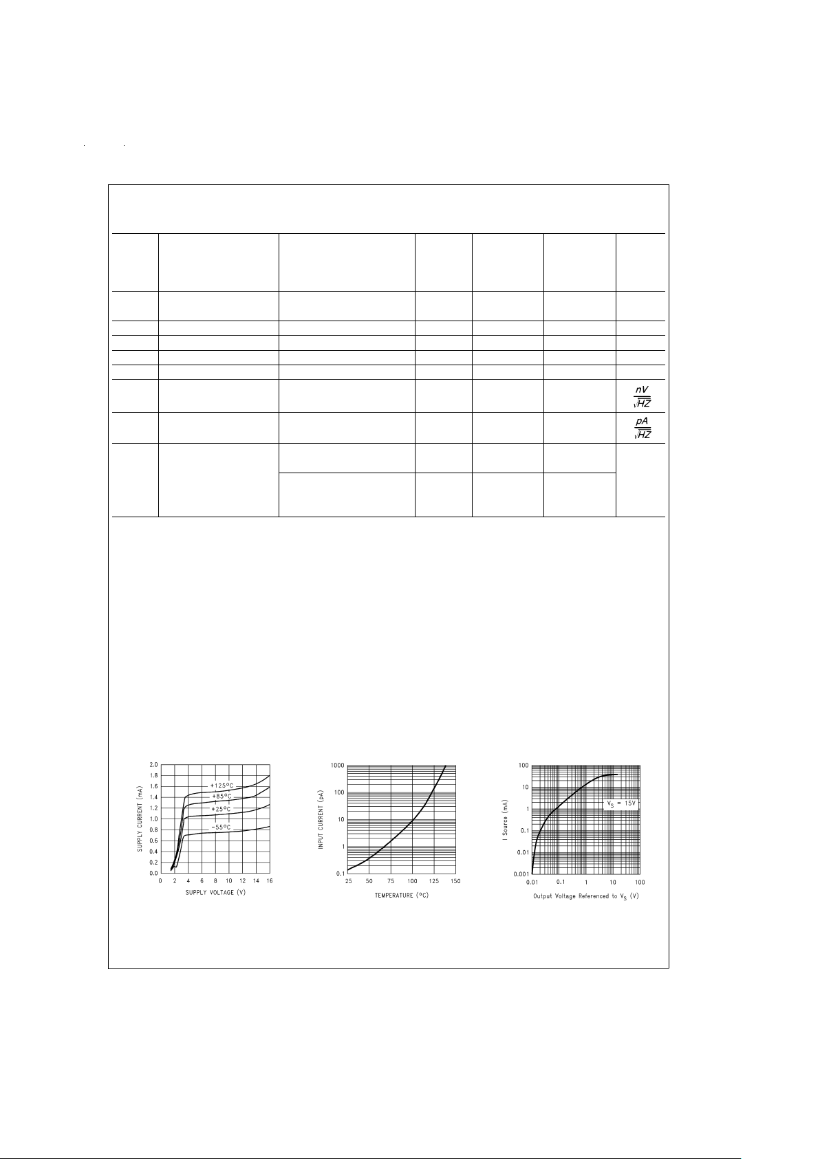
DC Electrical Characteristics
Unless otherwise specified, all limits guaranteed for T
J
=
25˚C, V
+
=
5V, V
−
=
0V, V
CM
=
V
O
=
V
+
/2 and R
L
>
1MΩ.Bold-
face limits apply at the temperature extremes
LMC6492AE LMC6492BE
Symbol Parameter Conditions Typ LMC6494AE LMC6494BE Units
(Note 5) Limit Limit
(Note 6) (Note 6)
V
OS
Input Offset Voltage 0.11 3.0 6.0 mV
3.8 6.8 max
TCV
OS
Input Offset Voltage 1.0 µV/˚C
Average Drift
I
B
Input Bias Current (Note 11) 0.15 200 200 pA max
I
OS
Input Offset Current (Note 11) 0.075 100 100 pA max
R
IN
Input Resistance
>
10 Tera Ω
C
IN
Common-Mode 3 pF
Input Capacitance
CMRR Common-Mode 0V ≤ V
CM
≤ 15V 82 65 63 dB
min
Rejection Ratio V
+
=
15V 60 58
0V ≤ V
CM
≤ 5V 82 65 63
60 58
+PSRR Positive Power Supply 5V ≤ V
+
≤ 15V, 82 65 63 dB
Rejection Ratio V
O
=
2.5V 60 58 min
−PSRR Negative Power Supply 0V ≤ V
−
≤ −10V, 82 65 63 dB
Rejection Ratio V
O
=
2.5V 60 58 min
V
CM
Input Common-Mode V
+
=
5V and 15V V
−
−0.3 −0.25 −0.25 V
Voltage Range For CMRR ≥ 50 dB 00max
V
+
+ 0.3 V++ 0.25 V++ 0.25 V
V
+
V
+
min
A
V
Large Signal Voltage Gain R
L
=
2kΩ: Sourcing 300 V/mV
(Note 7) Sinking 40 min
www.national.com3
DC Electrical Characteristics (Continued)
Unless otherwise specified, all limits guaranteed for T
J
=
25˚C, V
+
=
5V, V
−
=
0V, V
CM
=
V
O
=
V
+
/2 and R
L
>
1MΩ.Bold-
face limits apply at the temperature extremes
LMC6492AE LMC6492BE
Symbol Parameter Conditions Typ LMC6494AE LMC6494BE Units
(Note 5) Limit Limit
(Note 6) (Note 6)
V
O
Output Swing V
+
=
5V 4.9 4.8 4.8 V
R
L
=
2kΩto V
+
/2 4.7 4.7 min
0.1 0.18 0.18 V
0.24 0.24 max
V
+
=
5V 4.7 4.5 4.5 V
R
L
=
600Ω to V
+
/2 4.24 4.24 min
0.3 0.5 0.5 V
0.65 0.65 max
V
+
=
15V 14.7 14.4 14.4 V
R
L
=
2kΩto V
+
/2 14.0 14.0 min
0.16 0.35 0.35 V
0.5 0.5 max
V
+
=
15V 14.1 13.4 13.4 V
R
L
=
600Ω to V
+
/2 13.0 13.0 min
0.5 1.0 1.0 V
1.5 1.5 max
I
SC
Output Short Circuit Current Sourcing, V
O
=
0V 25 16 16
mA
min
10 10
V
+
=
5V Sinking, V
O
=
5V 22 11 11
88
I
SC
Output Short Circuit Current Sourcing, V
O
=
0V 30 28 28
20 20
V
+
=
15V Sinking, V
O
=
5V
(Note 8)
30 30 30
22 22
I
S
Supply Current LMC6492 1.0 1.75 1.75 mA
V
+
=
+5V, V
O
=
V
+
/2 2.1 2.1 max
LMC6492 1.3 1.95 1.95 mA
V
+
=
+15V, V
O
=
V
+
/2 2.3 2.3 max
LMC6494 2.0 3.5 3.5 mA
V
+
=
+5V, V
O
=
V
+
/2 4.2 4.2 max
LMC6494 2.6 3.9 3.9 mA
V
+
=
+15V, V
O
=
V
+
/2 4.6 4.6 max
www.national.com 4
AC Electrical Characteristics
Unless otherwise specified, all limits guaranteed for T
J
=
25˚C, V
+
=
5V, V
−
=
0V, V
CM
=
V
O
=
V
+
/2 and R
L
>
1MΩ.Bold-
face limits apply at the temperature extremes
LMC6492AE LMC6492BE
Symbol Parameter Conditions Typ LMC6494AE LMC6494BE Units
(Note 5) Limit Limit
(Note 6) (Note 6)
SR Slew Rate (Note 9) 1.3 0.7 0.7 Vµs min
0.5 0.5
GBW Gain-Bandwidth Product V
+
=
15V 1.5 MHz
φ
m
Phase Margin 50 Deg
G
m
Gain Margin 15 dB
Amp-to-Amp Isolation (Note 10) 150 dB
e
n
Input-Referred F=1 kHz
37
Voltage Noise V
CM
=
1V
i
n
Input-Referred F=1 kHz
0.06
Current Noise
T.H.D. Total Harmonic
Distortion
F=1 kHz, A
V
=
−2 0.01
%
R
L
=
10 kΩ,V
O
=
−4.1 V
PP
F=10 kHz, A
V
=
−2
R
L
=
10 kΩ,V
O
=
8.5 V
PP
0.01
V
+
=
10V
Note 1: Absolute Maximum Ratings indicate limits beyond which damage to the device may occur. Operating Ratings indicate conditions for which the device is intended to be functional, but specific performance is not guaranteed. For guaranteed specifications and the test conditions, see the Electrical Characteristics.
Note 2: Human body model, 1.5 kΩ in series with 100 pF.
Note 3: Applies to both single-supply and split-supply operation. Continuous short operation at elevated ambient temperature can result in exceeding the maximum
allowed junction temperature at 150˚C. Output currents in excess of
±
30 mA over long term may adversely affect reliability.
Note 4: The maximum power dissipation is a function of T
J(max)
, θJAand TA. The maximum allowable power dissipation at any ambient temperature is P
D
=
(T
J(max)
−TA)/θJA. All numbers apply for packages soldered directly into a PC board.
Note 5: Typical Values represent the most likely parametric norm.
Note 6: All limits are guaranteed by testing or statistical analysis.
Note 7: V
+
=
15V, V
CM
=
7.5V and R
L
connected to 7.5V. For Sourcing tests, 7.5V ≤ VO≤ 11.5V. For Sinking tests, 3.5V ≤ VO≤ 7.5V.
Note 8: Do not short circuit output to V
+
, when V+is greater than 13V or reliability will be adversely affected.
Note 9: V
+
=
15V. Connected as voltage follower with 10V step input. Number specified is the slower of the positive and negative slew rates.
Note 10: Input referred, V
+
=
15V and R
L
=
100 kΩ connected to 7.5V. Each amp excited in turn with 1 kHz to produce V
O
=
12 V
PP
.
Note 11: Guaranteed limits are dictated by tester limits and not device performance. Actual performance is reflected in the typical value.
Typical Performance Characteristics V
S
=
+15V, Single Supply, T
A
=
25˚C unless otherwise
specified
Supply Current vs
Supply Voltage
DS012049-25
Input Current vs
Temperature
DS012049-26
Sourcing Current vs
Output Voltage
DS012049-27
www.national.com5
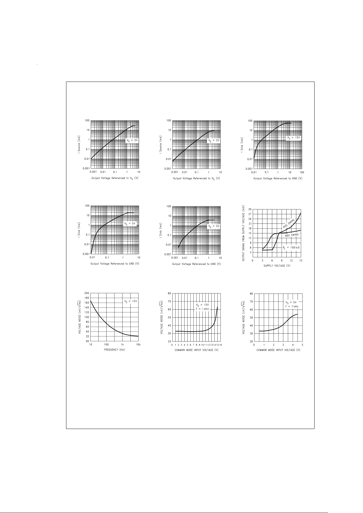
Typical Performance Characteristics V
S
=
+15V, Single Supply, T
A
=
25˚C unless otherwise
specified (Continued)
Sourcing Current vs
Output Voltage
DS012049-28
Sourcing Current vs
Output Voltage
DS012049-29
Sinking Current vs
Output Voltage
DS012049-30
Sinking Current vs
Output Voltage
DS012049-31
Sinking Current vs
Output Voltage
DS012049-32
Output Voltage Swing vs
Supply Voltage
DS012049-33
Input Voltage Noise
vs Frequency
DS012049-34
Input Voltage Noise
vs Input Voltage
DS012049-35
Input Voltage Noise
vs Input Voltage
DS012049-36
www.national.com 6
 Loading...