

NSC LF442MH-883, LF442AMH, LF442MWC, LF442CN, LF442ACN Datasheet

LF442
Dual Low Power JFET Input Operational Amplifier
General Description
The LF442 dual low power operational amplifiers provide
many of the same AC characteristics as the industry standard LM1458 while greatly improving the DC characteristics
of the LM1458. The amplifiers have the same bandwidth,
slew rate, and gain (10 kΩ load) as the LM1458 and only
draw one tenth thesupplycurrent of the LM1458. In addition
the well matched high voltage JFET input devices of the
LF442 reduce the input bias and offset currents by a factor of
10,000 over the LM1458. A combination of careful layout design and internal trimming guarantees very low input offset
voltage and voltage drift. The LF442 also has a very low
equivalent input noise voltage for a low power amplifier.
The LF442 is pin compatible with the LM1458 allowing an
immediate 10 times reduction in power drain in many applications. The LF442 should be used where low power dissipation and good electrical characteristics are the major considerations.
Features
n 1/10 supply current of a LM1458: 400 µA (max)
n Low input bias current: 50 pA (max)
n Low input offset voltage: 1 mV (max)
n Low input offset voltage drift: 10 µV/˚C (max)
n High gain bandwidth: 1 MHz
n High slew rate: 1 V/µs
n Low noise voltage for low power:
n Low input noise current:
n High input impedance: 1012Ω
n High gain V
O
=
±
10V, R
L
=
10k: 50k (min)
Typical Connection
Ordering Information
LF442XYZ
X indicates electrical grade
Y indicates temperature range
“M” for military
“C” for commercial
Z indicates package type
“H” or “N”
Connection Diagrams
BI-FET II™is a trademark of National Semiconductor Corporation.
DS009155-1
Metal Can Package
DS009155-2
Pin 4 connected to case
Top View
Order Number LF442AMH or LF442MH
or LF442MH/883
See NS Package Number H08A
Dual-In-Line Package
DS009155-4
Top View
Order Number LF442ACN or LF442CN
See NS Package Number N08E
April 1999
LF442 Dual Low Power JFET Input Operational Amplifier
© 1999 National Semiconductor Corporation DS009155 www.national.com
Absolute Maximum Ratings (Note 1)
If Military/Aerospace specified devices are required,
please contact the National Semiconductor Sales Office/
Distributors for availability and specifications.
LF442A LF442
Supply Voltage
±
22V
±
18V
Differential Input Voltage
±
38V
±
30V
Input Voltage Range
±
19V
±
15V
(Note 2)
Output Short Circuit Continuous Continuous
Duration (Note 3)
H Package N Package
T
j
max 150˚C 115˚C
H Package N Package
θ
JA
(Typical)
(Note 4)
(Note 5)
65˚C/W
165˚C/W
114˚C/W
152˚C/W
θ
JC
(Typical) 21˚C/W
Operating Temperature (Note 5) (Note 5)
Range
Storage −65˚C≤T
A
≤150˚C −65˚C≤TA≤150˚C
Temperature Range
Lead Temperature 260˚C 260˚C
(Soldering, 10 sec.)
ESD Tolerance Rating to be determined
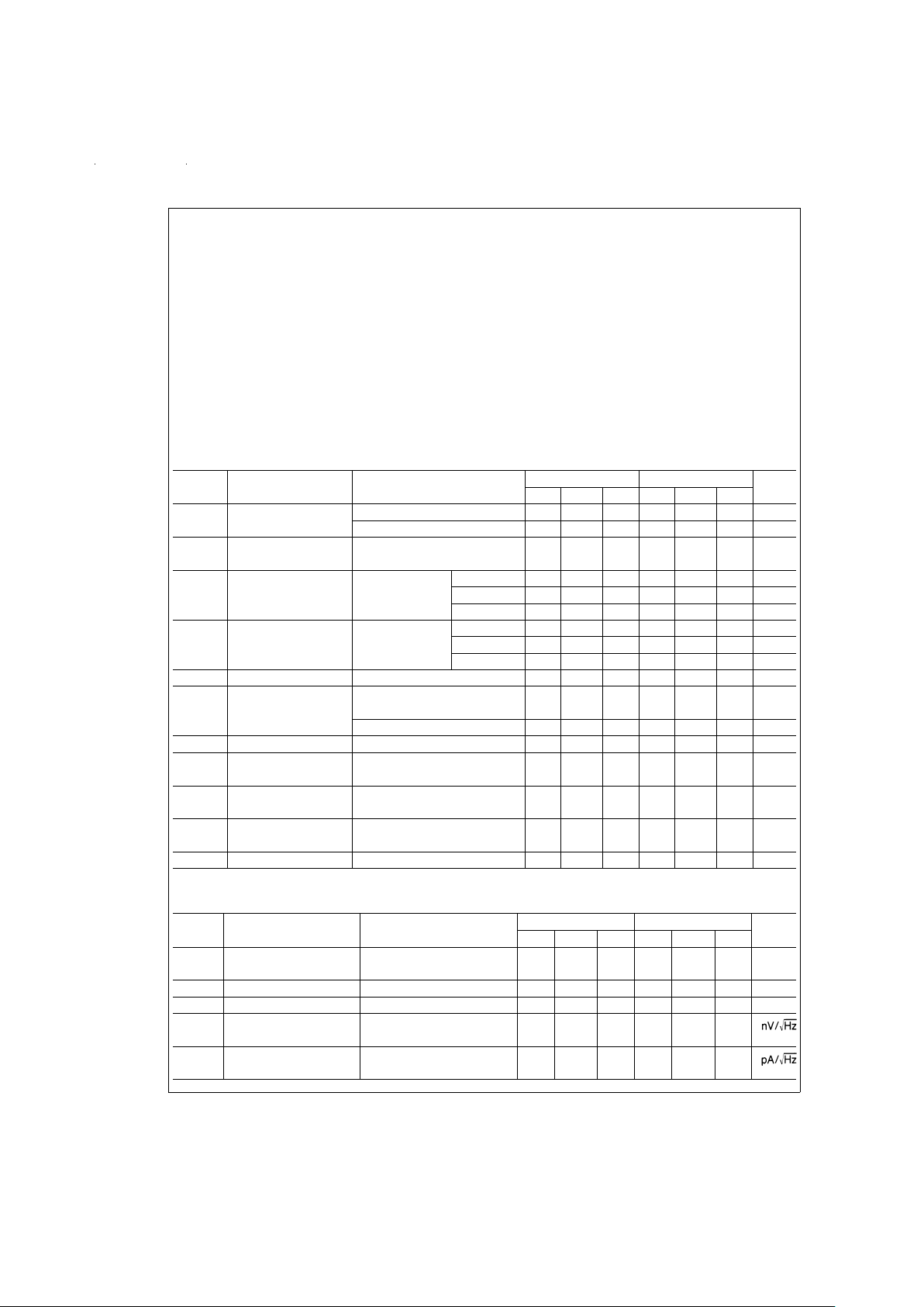
DC Electrical Characteristics (Note 7)
Symbol Parameter Conditions LF442A LF442 Units
Min Typ Max Min Typ Max
V
OS
Input Offset Voltage R
S
=
10 kΩ,T
A
=
25˚C 0.5 1.0 1.0 5.0 mV
Over Temperature 7.5 mV
∆V
OS
/∆T Average TC of Input R
S
=
10 kΩ 7 10 7 µV/˚C
Offset Voltage
I
OS
Input Offset Current V
S
=
±
15V T
j
=
25˚C 5 25 5 50 pA
(Notes 7, 8) T
j
=
70˚C 1.5 1.5 nA
T
j
=
125˚C 10 nA
I
B
Input Bias Current V
S
=
±
15V T
j
=
25˚C 10 50 10 100 pA
(Notes 7, 8) T
j
=
70˚C 3 3 nA
T
j
=
125˚C 20 nA
R
IN
Input Resistance T
j
=
25˚C 10
12
10
12
Ω
A
VOL
Large Signal Voltage V
S
=
±
15V, V
O
=
±
10V, 50 200 25 200 V/mV
Gain R
L
=
10 kΩ,T
A
=
25˚C
Over Temperature 25 200 15 200 V/mV
V
O
Output Voltage Swing V
S
=
±
15V, R
L
=
10 kΩ
±
12±13
±
12±13 V
V
CM
Input Common-Mode
±
16 +18
±
11 +14 V
Voltage Range −17 −12 V
CMRR Common-Mode R
S
≤ 10 kΩ 80 100 70 95 dB
Rejection Ratio
PSRR Supply Voltage (Note 9) 80 100 70 90 dB
Rejection Ratio
I
S
Supply Current 300 400 400 500 µA
AC Electrical Characteristics (Note 7)
Symbol Parameter Conditions LF442A LF442 Units
Min Typ Max Min Typ Max
Amplifier to Amplifier T
A
=
25˚C, f=1 Hz-20 kHz −120 −120 dB
Coupling (Input Referred)
SR Slew Rate V
S
=
±
15V, T
A
=
25˚C 0.8 1 0.6 1 V/µs
GBW Gain-Bandwidth Product V
S
=
±
15V, T
A
=
25˚C 0.8 1 0.6 1 MHz
e
n
Equivalent Input Noise T
A
=
25˚C, R
S
=
100Ω,35 35
Voltage f=1 kHz
i
n
Equivalent Input Noise T
A
=
25˚C, f=1 kHz 0.01 0.01
Current
www.national.com 2

AC Electrical Characteristics (Note 7) (Continued)
Note 1: “Absolute Maximum Ratings” indicate limits beyond which damage to the device may occur. Operating Ratings indicate conditions for which the device is
functional, but do not guarantee specific performance limits.
Note 2: Unless otherwise specified the absolute maximum negative input voltage is equal to the negative power supply voltage.
Note 3: Any of the amplifier outputs can be shorted to ground indefinitely, however, more than one should not be simultaneously shorted as the maximum junction
temperature will be exceeded.
Note 4: The value given is in 400 linear feet/min air flow.
Note 5: The value given is in static air.
Note 6: These devices are available in both the commercial temperature range 0˚C ≤ T
A
≤ 70˚C and the military temperature range −55˚C ≤ TA≤ 125˚C. The temperature range is designated by the position just before the package type in the device number. A “C” indicates the commercial temperature range and an “M” indicates the military temperature range. The military temperature range is available in “H” package only.
Note 7: Unless otherwise specified, the specifications apply over the full temperature range and for V
S
=
±
20V for the LF442A and for V
S
=
±
15V for the LF442.
V
OS,IB
, and IOSare measured at V
CM
=
0.
Note 8: The input bias currents are junction leakage currents which approximately double for every 10˚C increase in the junction temperature, T
j
. Due to limited production test time, the input bias currents measured are correlated to junction temperature. In normal operation the junction temperature rises above the ambient temperature as a result of internal power dissipation, P
D.Tj
=
T
A+θjAPD
where θjAis the thermal resistance from junction to ambient. Use of a heat sink is recommended
if input bias current is to be kept to a minimum.
Note 9: Supply voltage rejection ratio is measured for both supply magnitudes increasing or decreasing simultaneously in accordance with common practice from
±
15V to±5V for the LF442 and±20V to±5V for the LF442A.
Note 10: Refer to RETS442X for LF442MH military specifications.
Typical Performance Characteristics
Input Bias Current
DS009155-17
Input Bias Current
DS009155-18
Supply Current
DS009155-19
Positive Common-Mode
Input Voltage Limit
DS009155-20
Negative Common-Mode
Input Voltage Limit
DS009155-21
Positive Current Limit
DS009155-22
www.national.com3
Typical Performance Characteristics (Continued)
Negative Current Limit
DS009155-23
Output Voltage Swing
DS009155-24
Output Voltage Swing
DS009155-25
Gain Bandwidth
DS009155-26
Bode Plot
DS009155-27
Slew Rate
DS009155-28
Distortion vs Frequency
DS009155-29
Undistorted Output Voltage
Swing
DS009155-30
Open Loop Frequency
Response
DS009155-31
www.national.com 4
 Loading...