

DS90C401
Dual Low Voltage Differential Signaling (LVDS) Driver
General Description
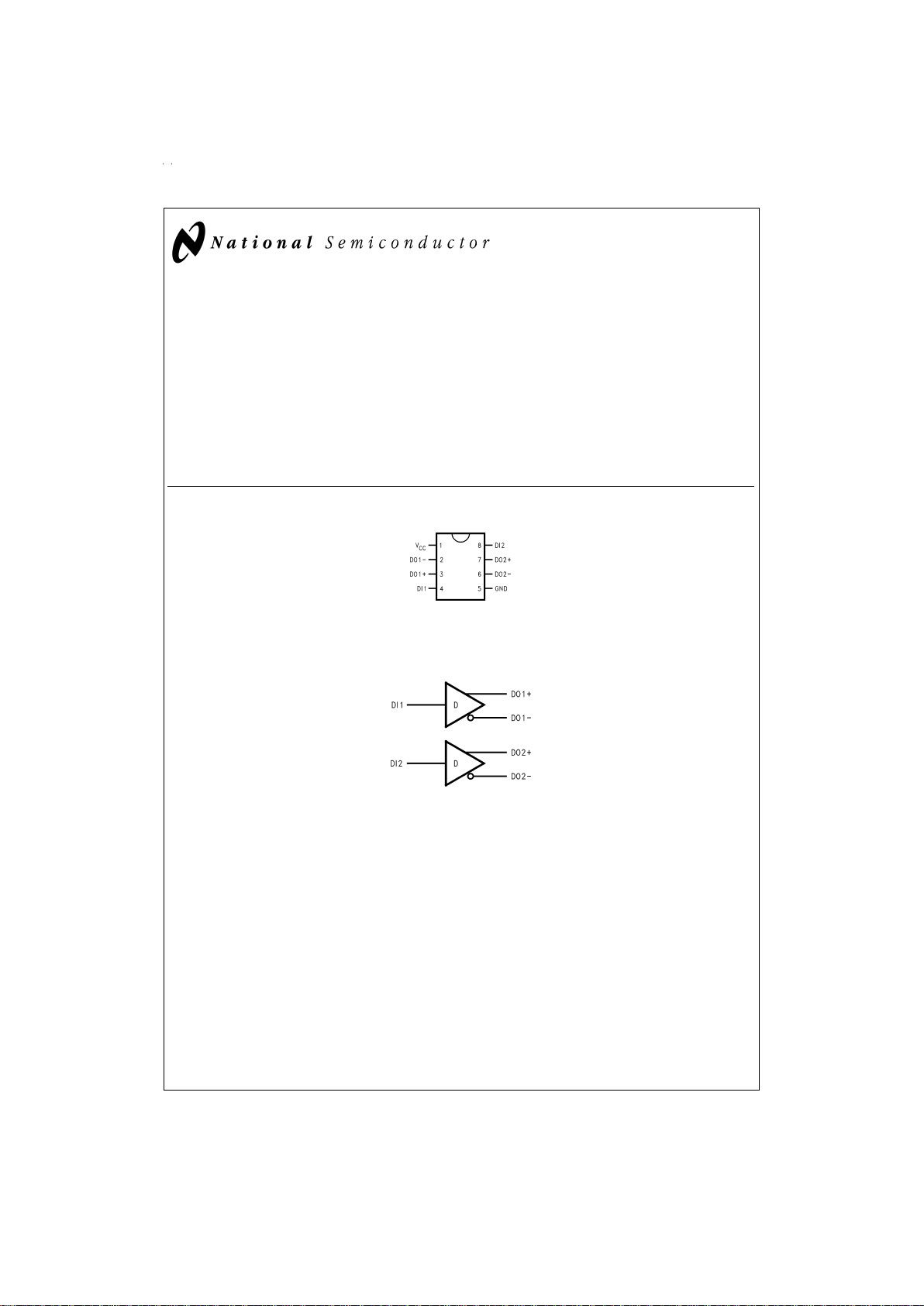
The DS90C401 is a dual driver device optimized for high
data rate and low power applications. This device along with
the DS90C402 provides a pair chip solution for a dual high
speed point-to-point interface. The DS90C401 is a current
mode driverallowingpower dissipation to remain low even at
high frequency. In addition, the short circuit fault current is
also minimized. The device is in a 8 lead small outline package. The differential driver outputs provides low EMI with its
low output swings typically 340 mV.
Features
n Ultra low power dissipation
n Operates above 155.5 Mbps
n Standard TIA/EIA-644
n 8 Lead SOIC Package saves space
n Low Differential Output Swing typical 340 mV
Connection Diagram
Functional Diagram
DS100013-1
Order Number DS90C401M
See NS Package Number M08A
DS100013-2
June 1998
DS90C401 Dual Low Voltage Differential Signaling (LVDS) Driver
© 1998 National Semiconductor Corporation DS100013 www.national.com
Absolute Maximum Ratings (Note 1)
If Military/Aerospace specified devices are required,
please contact the National Semiconductor Sales Office/
Distributors for availability and specifications.
Supply Voltage (V
CC
) −0.3V to +6V
Input Voltage (D
IN
) −0.3V to (VCC+ 0.3V)
Output Voltage (D
OUT+,DOUT−
) −0.3V to (VCC+ 0.3V)
Short Circuit Duration
(D
OUT+,DOUT−
) Continuous
Maximum Package Power Dissipation
@
+25˚C
M Package 1068 mW
Derate M Package 8.5 mW/˚C above +25˚C
Storage Temperature Range −65˚C to +150˚C
Lead Temperature Range
Soldering (4 sec.) +260˚C
Maximum Junction Temperature +150˚C
ESD Rating
(HBM, 1.5 kΩ, 100 pF) ≥ 3,500V
(EIAJ, 0 Ω, 200 pF) ≥ 250V
Recommended Operating
Conditions
Min Typ Max Units
Supply Voltage (V
CC
) +4.5 +5.0 +5.5 V
Operating Free Air
Temperature (T
A
) −40 +25 +85 ˚C
Electrical Characteristics
Over supply voltage and operating temperature ranges, unless otherwise specified. (Notes 2, 3)
Symbol Parameter Conditions Pin Min Typ Max Units
V
OD1
Differential Output Voltage RL= 100Ω (
Figure 1
)D
OUT−
,
D
OUT+
250 340 450 mV
∆V
OD1
Change in Magnitude of V
OD1
for Complementary Output
States
4 35 |mV|
V
OS
Offset Voltage 1.125 1.25 1.375 V
∆V
OS
Change in Magnitude of VOSfor
Complementary Output States
5 25 |mV|
V
OH
Output Voltage High RL= 100Ω 1.41 1.60 V
V
OL
Output Voltage Low 0.90 1.07 V
I
OS
Output Short Circuit Current V
OUT
= 0V (Note 8) −3.5 −5.0 mA
V
IH
Input Voltage High D
IN
2.0 V
CC
V
V
IL
Input Voltage Low GND 0.8 V
I
I
Input Current VIN=VCC, GND, 2.5V or 0.4V −10
±
1 +10 µA
V
CL
Input Clamp Voltage ICL= −18 mA −1.5 −0.8 V
I
CC
No Load Supply Current DIN=VCCor GND V
CC
1.7 3.0 mA
D
IN
= 2.5V or 0.4V 3.5 5.5 mA
I
CCL
Loaded Supply Current RL= 100Ω All Channels
V
IN=VCC
or GND (all inputs)
8 14.0 mA
Switching Characteristics
VCC= +5.0V±10%,TA= −40˚C to +85˚C (Notes 3, 4, 5, 6, 9)
Symbol Parameter Conditions Min Typ Max Units
t
PHLD
Differential Propagation Delay High to Low RL= 100Ω,CL=5pF
(
Figure 2
and
Figure 3
)
0.5 2.0 3.5 ns
t
PLHD
Differential Propagation Delay Low to High 0.5 2.1 3.5 ns
t
SKD
Differential Skew |t
PHLD–tPLHD
| 0 80 900 ps
t
SK1
Channel-to-Channel Skew (Note 4) 0 0.3 1.0 ns
t
SK2
Chip to Chip Skew (Note 5) 3.0 ns
t
TLH
Rise Time 0.35 2.0 ns
t
THL
Fall Time 0.35 2.0 ns
www.national.com 2
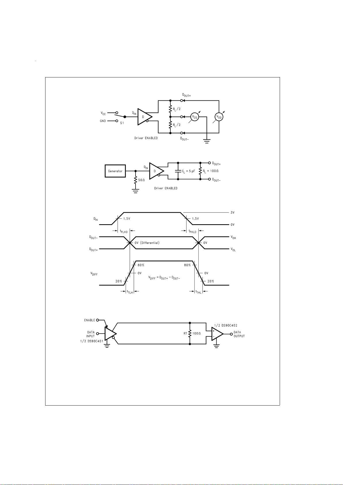
Parameter Measurement Information
Typical Application
Applications Information
LVDSdrivers and receivers are intended to be primarily used
in an uncomplicated point-to-point configuration as is shown
in
Figure 4
. This configuration provides a clean signaling environment for the quick edge rates of the drivers. The receiver is connected to the driver through a balanced media
which may be a standard twisted pair cable, a parallel pair
cable, or simply PCB traces. Typically, the characteristic im-
pedance of the media is in the range of 100Ω. A termination
resistor of 100Ω should be selected to match the media, and
is located as close to the receiver input pins as possible. The
termination resistor converts the current sourced by the
driver into a voltage that is detected by the receiver. Other
configurations are possible such as a multi-receiver configuration, but the effects of a mid-stream connector(s), cable
DS100013-4
FIGURE 1. Driver VODand VOSTest Circuit
DS100013-5
FIGURE 2. Driver Propagation Delay and Transition Time Test Circuit
DS100013-6
FIGURE 3. Driver Propagation Delay and Transition Time Waveforms
DS100013-9
FIGURE 4. Point-to-Point Application
www.national.com3
 Loading...