

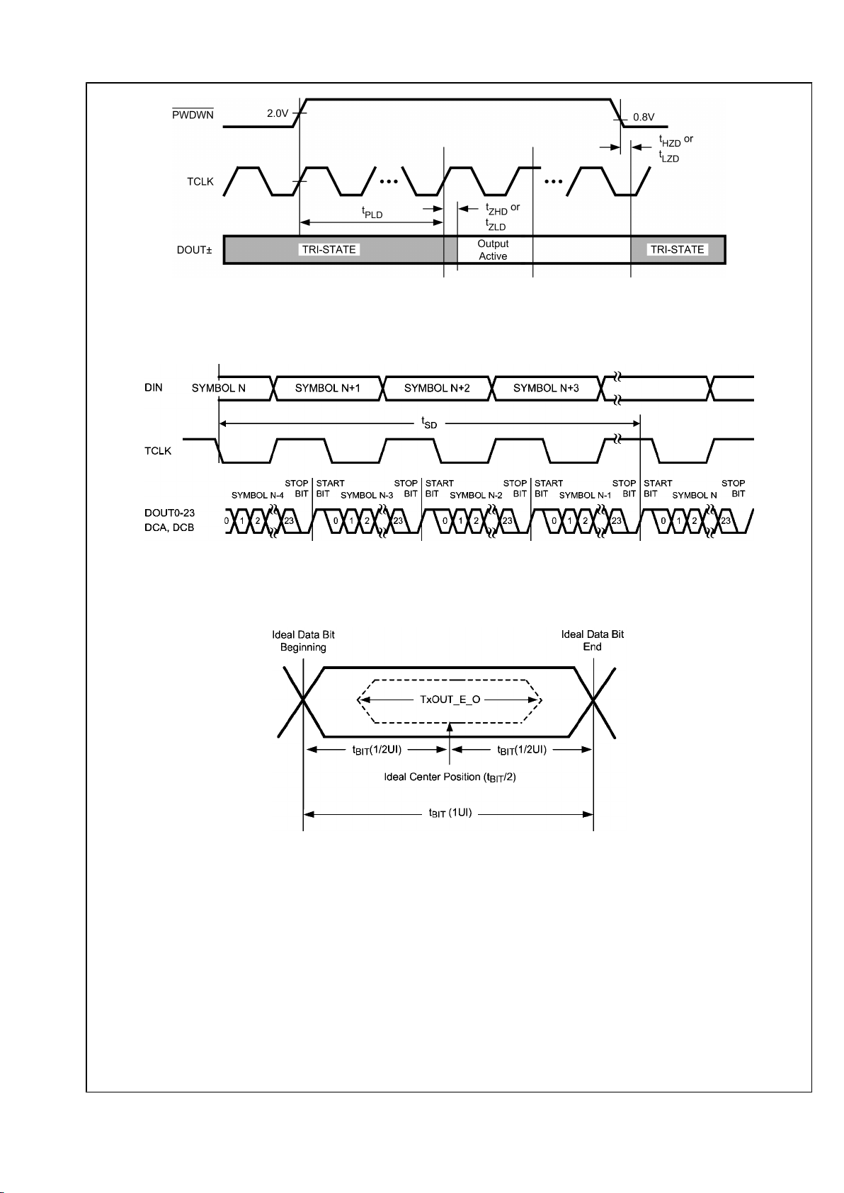
November 21, 2007
DS90C241/DS90C124
5-35MHz DC-Balanced 24-Bit LVDS Serializer and
Deserializer
General Description
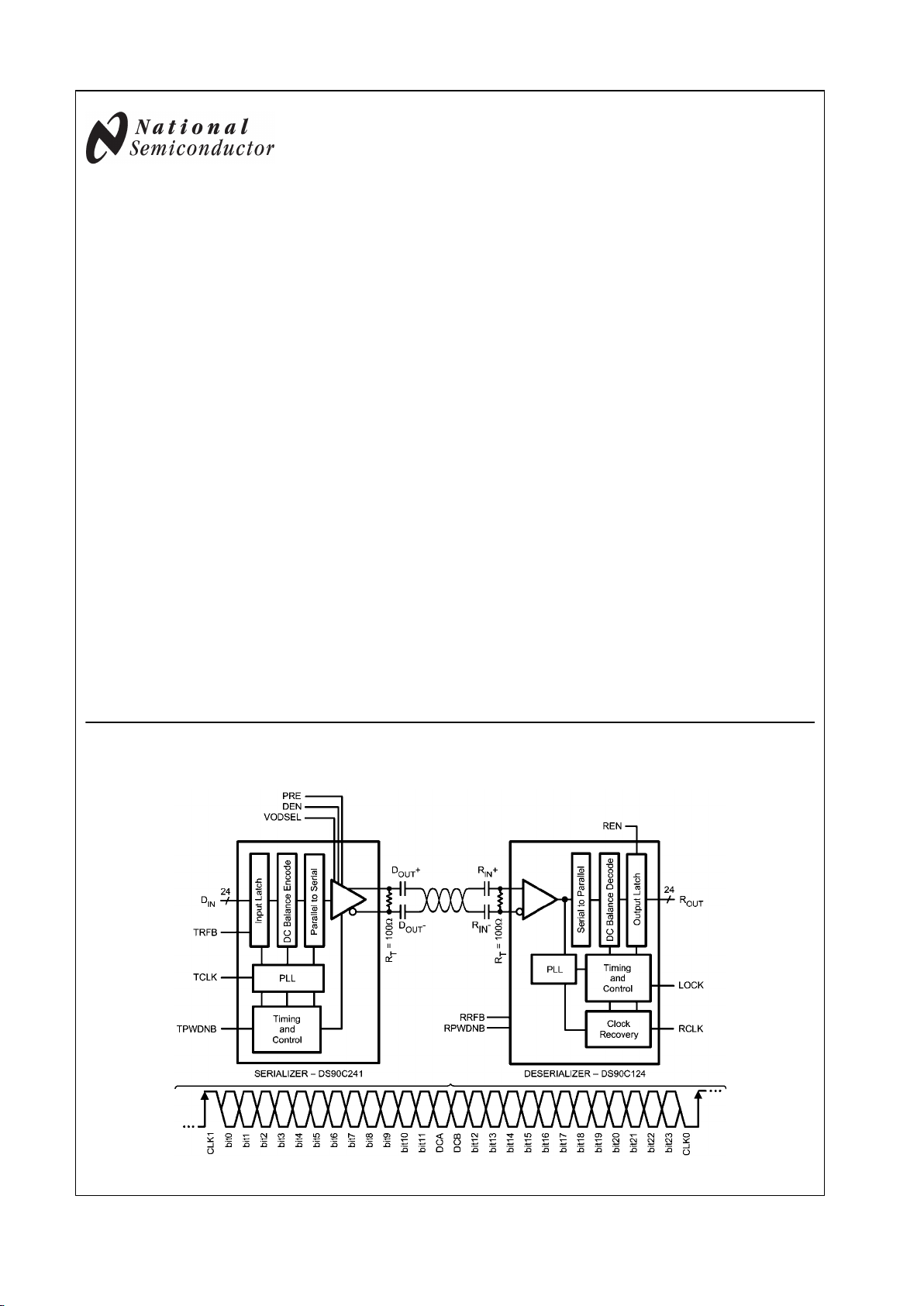
The DS90C241/DS90C124 Chipset translates a 24-bit parallel bus into a fully transparent data/control LVDS serial stream
with embedded clock information. This single serial stream
simplifies transferring a 24-bit bus over PCB traces and cable
by eliminating the skew problems between parallel data and
clock paths. It saves system cost by narrowing data paths that
in turn reduce PCB layers, cable width, and connector size
and pins.
The DS90C241/DS90C124 incorporates LVDS signaling on
the high-speed I/O. LVDS provides a low power and low noise
environment for reliably transferring data over a serial transmission path. By optimizing the serializer output edge rate for
the operating frequency range EMI is further reduced.
In addition the device features pre-emphasis to boost signals
over longer distances using lossy cables. Internal DC balanced encoding/decoding is used to support AC-Coupled
interconnects.
Features
■
5 MHz–35 MHz clock embedded and DC-Balancing 24:1
and 1:24 data transmissions
■
User defined Pre-Emphasis driving ability through external
resistor on LVDS outputs and capable to drive up to 10
meters shielded twisted-pair cable
■
User selectable clock edge for parallel data on both
Transmitter and Receiver
■
Internal DC Balancing encode/decode – Supports ACcoupling interface with no external coding required
■
Individual power-down controls for both Transmitter and
Receiver
■
Embedded clock CDR (clock and data recovery) on
Receiver and no external source of reference clock
needed
■
All codes RDL (random data lock) to support livepluggable applications
■
LOCK output flag to ensure data integrity at Receiver side
■
Balanced T
SETUP/THOLD
between RCLK and RDATA on
Receiver side
■
PTO (progressive turn-on) LVCMOS outputs to reduce
EMI and minimize SSO effects
■
All LVCMOS inputs and control pins have internal
pulldown
■
On-chip filters for PLLs on Transmitter and Receiver
■
Temperature range –40°C to +105°C
■
Greater than 8 kV HBM ESD tolerant
■
Meets AEC-Q100 compliance
■
Power supply range 3.3V ± 10%
■
48-pin TQFP package
Block Diagram
20171901
TRI-STATE® is a registered trademark of National Semiconductor Corporation.
© 2007 National Semiconductor Corporation 201719 www.national.com
DS90C241/DS90C124 5-35MHz DC-Balanced 24-Bit LVDS Serializer and Deserializer
Absolute Maximum Ratings (Note 1)
If Military/Aerospace specified devices are required,
please contact the National Semiconductor Sales Office/
Distributors for availability and specifications.
Supply Voltage (VCC)
−0.3V to +4V
LVCMOS/LVTTL Input Voltage −0.3V to (VCC +0.3V)
LVCMOS/LVTTL Output Voltage −0.3V to (V
CC
+0.3V)
LVDS Receiver Input Voltage −0.3V to 3.9V
LVDS Driver Output Voltage −0.3V to 3.9V
LVDS Output Short Circuit Duration 10 ms
Junction Temperature +150°C
Storage Temperature −65°C to +150°C
Lead Temperature
(Soldering, 4 seconds) +260°C
Maximum Package Power Dissipation Capacity Package
De-rating:
48L TQFP
1/θJA °C/W above +25°C
DS90C241
θ
JA
45.8 (4L*); 75.4 (2L*) °C/W
θ
JC
21.0°C/W
DS90C124
θ
JA
45.4 (4L*); 75.0 (2L*)°C/W
θ
JC
21.1°C/W
*JEDEC
ESD Rating (HBM)
≥±8 kV
ESD Rating (ISO10605) DS90C241 meets ISO 10605
RD = 2 kΩ, CS = 330 pF
Contact Discharge (D
OUT+
, D
OUT-
)
±8 kV
Air Discharge (D
OUT+
, D
OUT-
)
±25 kV
Recommended Operating
Conditions
Min Nom Max Units
Supply Voltage (VCC) 3.0 3.3 3.6 V
Operating Free Air
Temperature (TA)
−40 +25 +105 °C
Clock Rate 5 35 MHz
Supply Noise ±100 mV
P-P
Electrical Characteristics
Over recommended operating supply and temperature ranges unless otherwise specified.
Symbol Parameter Conditions Pin/Freq. Min Typ Max Units
LVCMOS/LVTTL DC SPECIFICATIONS
V
IH
High Level Voltage Tx: DIN[23:0], TCLK,
TPWDNB, DEN, TRFB,
DCAOFF, DCBOFF,
VODSEL
Rx: RPWDNB, RRFB,
REN
2.0
V
CC
V
V
IL
Low Level Input Voltage
GND 0.8 V
V
CL
Input Clamp Voltage ICL = −18 mA
(Note 9)
−0.8 −1.5 V
I
IN
Input Current VIN = 0V or 3.6V Tx: DIN[23:0], TCLK,
TPWDNB, DEN, TRFB,
DCAOFF, DCBOFF,
VODSEL
−10 ±5 +10 µA
Rx: RPWDNB, RRFB,
REN
−20 ±5 +20 µA
V
OH
High Level Output Voltage IOH = −4 mA Rx: ROUT[23:0], RCLK,
LOCK
2.3 3.0
V
CC
V
V
OL
Low Level Output Voltage IOL = +4 mA
GND 0.33 0.5 V
I
OS
Output Short Circuit Current V
OUT
= 0V
(Note 9)
−40 −70 −110 mA
I
OZ
TRI-STATE® Output Current RPWDNB, REN = 0V
V
OUT
= 0V or 2.4V
Rx: ROUT[23:0], RCLK,
LOCK
−30 ±0.4 +30 µA
LVDS DC SPECIFICATIONS
V
TH
Differential Threshold High
Voltage
VCM = +1.2V Rx: R
IN+
, R
IN−
+50 mV
V
TL
Differential Threshold Low
Voltage
−50 mV
I
IN
Input Current VIN = +2.4V,
VCC = 3.6V or 0V
±200 µA
VIN = 0V, VCC = 3.6V
±200 µA
www.national.com 2
DS90C241/DS90C124
Symbol Parameter Conditions Pin/Freq. Min Typ Max Units
V
OD
Output Differential Voltage
(D
OUT+
)–(D
OUT−
)
RL = 100Ω, w/o Pre-emphasis
VODSEL = L (Figure 10)
Tx: D
OUT+
, D
OUT−
250 400 600 mV
RL = 100Ω, w/o Pre-emphasis
VODSEL = H (Figure 10)
450 750 1200 mV
ΔV
OD
Output Differential Voltage
Unbalance
RL = 100Ω, w/o Pre-emphasis
10 50 mV
V
OS
Offset Voltage
RL = 100Ω, w/o Pre-emphasis
1.00 1.25 1.50 V
ΔV
OS
Offset Voltage Unbalance
RL = 100Ω, w/o Pre-emphasis
1 50 mV
I
OS
Output Short Circuit Current DOUT = 0V, DIN = H,
TPWDNB, DEN = 2.4V,
VODSEL = L
−2 −8 mA
DOUT = 0V, DIN = H,
TPWDNB, DEN = 2.4V,
VODSEL = H
−7 −13 mA
I
OZ
TRI-STATE Output Current TPWDNB, DEN = 0V,
DOUT = 0V or 2.4V
−15 ±1 +15 µA
SER/DES SUPPLY CURRENT (DVDD*, PVDD* and AVDD* pins) *Digital, PLL, and Analog VDDs
I
CCT
Serializer (Tx)
Total Supply Current
(includes load current)
RL = 100Ω
R
PRE
= OFF
VODSEL = H/L
Checker-board pattern (Figure 1)
f = 35 MHz
40 65 mA
RL = 100Ω
R
PRE
= 6 kΩ
VODSEL = H/L
Checker-board pattern (Figure 1)
f = 35 MHz
45 70 mA
Serializer (Tx)
Total Supply Current
(includes load current)
RL = 100Ω
R
PRE
= OFF
VODSEL = H/L
f = 35 MHz
40 65 mA
RL = 100Ω
R
PRE
= 6 kΩ
VODSEL = H/L
Random pattern
f = 35 MHz
45 70 mA
I
CCTZ
Serializer (Tx)
Supply Current Power-down
TPWDNB = 0V
(All other LVCMOS Inputs = 0V)
800 µA
I
CCR
Deserializer (Rx)
Total Supply Current
(includes load current)
CL = 8 pF LVCMOS Output
Checker-board pattern
(Figure 2)
f = 35 MHz
85 mA
Deserializer (Rx)
Total Supply Current
(includes load current)
CL = 8 pF LVCMOS Output
Random pattern
f = 35 MHz
80 mA
I
CCRZ
Deserializer (Rx)
Supply Current Power-down
RPWDNB = 0V
(All other LVCMOS Inputs = 0V,
R
IN+
/ R
IN-
= 0V)
50 µA
3 www.national.com
DS90C241/DS90C124
Serializer Timing Requirements for TCLK
Over recommended operating supply and temperature ranges unless otherwise specified.
Symbol Parameter Conditions Min Typ Max Units
t
TCP
Transmit Clock Period (Figure 5)
28.6 T 200 ns
t
TCIH
Transmit Clock High Time
0.4T 0.5T 0.6T ns
t
TCIL
Transmit Clock Low Time
0.4T 0.5T 0.6T ns
t
CLKT
TCLK Input Transition Time (Figure 4)
3 6 ns
t
JIT
TCLK Input Jitter (Note 10)
33
ps
(RMS)
Serializer Switching Characteristics
Over recommended operating supply and temperature ranges unless otherwise specified.
Symbol Parameter Conditions Min Typ Max Units
t
LLHT
LVDS Low-to-High Transition Time
RL = 100Ω, (Figure 3)
CL = 10 pF to GND
VODSEL = L
0.6 ns
t
LHLT
LVDS High-to-Low Transition Time
0.6 ns
t
DIS
DIN (23:0) Setup to TCLK
RL = 100Ω,
CL = 10 pF to GND
(Note 9)
5 ns
t
DIH
DIN (23:0) Hold from TCLK
5 ns
t
HZD
DOUT ± HIGH to TRI-STATE Delay
RL = 100Ω,
CL = 10 pF to GND
(Figure 6) (Note 5)
15 ns
t
LZD
DOUT ± LOW to TRI-STATE Delay
15 ns
t
ZHD
DOUT ± TRI-STATE to HIGH Delay
200 ns
t
ZLD
DOUT ± TRI-STATE to LOW Delay
200 ns
t
PLD
Serializer PLL Lock Time
RL = 100Ω, (Figure 7)
10 ms
t
SD
Serializer Delay
RL = 100Ω, (Figure 8)
VODSEL = L, TRFB = H
3.5T + 2.85
3.5T
+ 10
ns
RL = 100Ω, (Figure 8)
VODSEL = L, TRFB = L
3.5T + 2.85
3.5T
+ 10
ns
TxOUT_E_O TxOUT_Eye_Opening
(respect to ideal)
5–35 MHz
(Figure 9)
(Notes 9, 10, 14)
0.75
UI
(Note 11)
Deserializer Switching Characteristics
Over recommended operating supply and temperature ranges unless otherwise specified.
Symbol Parameter Conditions Pin/Freq. Min Typ Max Units
t
RCP
Receiver out Clock Period t
RCP
= t
TCP
(Note 9)
RCLK
28.6 200 ns
t
RDC
RCLK Duty Cycle RCLK
45 50 55 %
t
CLH
LVCMOS Low-to-High
Transition Time
CL = 8 pF
(lumped load)
(Figure 11)
ROUT [23:0],
LOCK, RCLK
2.5 3.5 ns
t
CHL
LVCMOS High-to-Low
Transition Time
2.5 3.5 ns
t
ROS
ROUT (7:0) Setup Data to
RCLK (Group 1)
(Figure 15) ROUT [7:0] (0.40)*
t
RCP
(29/56)*t
RCP
ns
t
ROH
ROUT (7:0) Hold Data to RCLK
(Group 1)
(0.40)*
t
RCP
(27/56)*t
RCP
ns
t
ROS
ROUT (15:8) Setup Data to
RCLK (Group 2)
(Figure 15) ROUT [15:8],
LOCK
(0.40)*
t
RCP
0.5*t
RCP
ns
t
ROH
ROUT (15:8) Hold Data to
RCLK (Group 2)
(0.40)*
t
RCP
0.5*t
RCP
ns
www.national.com 4
DS90C241/DS90C124
Symbol Parameter Conditions Pin/Freq. Min Typ Max Units
t
ROS
ROUT (23:16) Setup Data to
RCLK (Group 3)
(Figure 15) ROUT [23:16] (0.40)*
t
RCP
(27/56)*t
RCP
ns
t
ROH
ROUT (23:16) Hold Data to
RCLK (Group 3)
(0.40)*
t
RCP
(29/56)*t
RCP
ns
t
HZR
HIGH to TRI-STATE Delay (Figure 13) ROUT [23:0],
RCLK, LOCK
3 10 ns
t
LZR
LOW to TRI-STATE Delay
3 10 ns
t
ZHR
TRI-STATE to HIGH Delay
3 10 ns
t
ZLR
TRI-STATE to LOW Delay
3 10 ns
t
DD
Deserializer Delay (Figure 12) RCLK
[4+(3/56)]T
+5.9
[4+(3/56)]T
+14
ns
t
DRDL
Deserializer PLL Lock Time
from Powerdown
(Figure 14)
(Notes 8, 9)
5 MHz 5 50 ms
35 MHz 5 50 ms
RxIN_TOL_L Receiver INput TOLerance
Left,
(Figure 16)
(Notes 7, 9, 11)
5 MHz–35 MHz
0.25 UI
RxIN_TOL_R Receiver INput TOLerance
Right,
(Figure 16)
(Notes 7, 9, 11)
5 MHz–35 MHz
0.25 UI
Note 1: “Absolute Maximum Ratings” indicate limits beyond which damage to the device may occur, including inoperability and degradation of device reliability
and/or performance. Functional operation of the device and/or non-degradation at the Absolute Maximum Ratings or other conditions beyond those indicated in
the Recommended Operating Conditions is not implied. The Recommended Operating Conditions indicate conditions at which the device is functional and the
device should not be operated beyond such conditions.
Note 2: The Electrical Characteristics tables list guaranteed specifications under the listed Recommended Operating Conditions except as otherwise modified
or specified by the Electrical Characteristics Conditions and/or Notes. Typical specifications are estimations only and are not guaranteed.
Note 3: Typical values represent most likely parametric norms at VCC = 3.3V, Ta = +25 degC, and at the Recommended Operation Conditions at the time of
product characterization and are not guaranteed.
Note 4: Current into device pins is defined as positive. Current out of a device pin is defined as negative. Voltages are referenced to ground except VOD, ΔVOD,
VTH and VTL which are differential voltages.
Note 5: When the Serializer output is tri-stated, the Deserializer will lose PLL lock. Resynchronization MUST occur before data transfer.
Note 6: t
DRDL
is the time required by the deserializer to obtain lock when exiting powerdown mode. t
DRDL
is specified with an external synchronization pattern.
Note 7: RxIN_TOL is a measure of how much phase noise (jitter) the deserializer can tolerate in the incoming data stream before bit errors occur. It is a
measurement in reference with the ideal bit position, please see National’s AN-1217 for detail.
Note 8: The Deserializer PLL lock time (t
DRDL
) may vary depending on input data patterns and the number of transitions within the pattern.
Note 9: Specification is guaranteed by characterization and is not tested in production.
Note 10: t
JIT
(@BER of 10e-9) specifies the allowable jitter on TCLK. t
JIT
not included in TxOUT_E_O parameter.
Note 11: UI – Unit Interval, equivalent to one ideal serialized data bit width. The UI scales with frequency.
Note 12: Figures 1, 2, 8, 12, 14 show a falling edge data strobe (TCLK IN/RCLK OUT).
Note 13: Figures , 15 show a rising edge data strobe (TCLK IN/RCLK OUT).
Note 14: TxOUT_E_O is affected by pre-emphasis value.
5 www.national.com
DS90C241/DS90C124
AC Timing Diagrams and Test Circuits
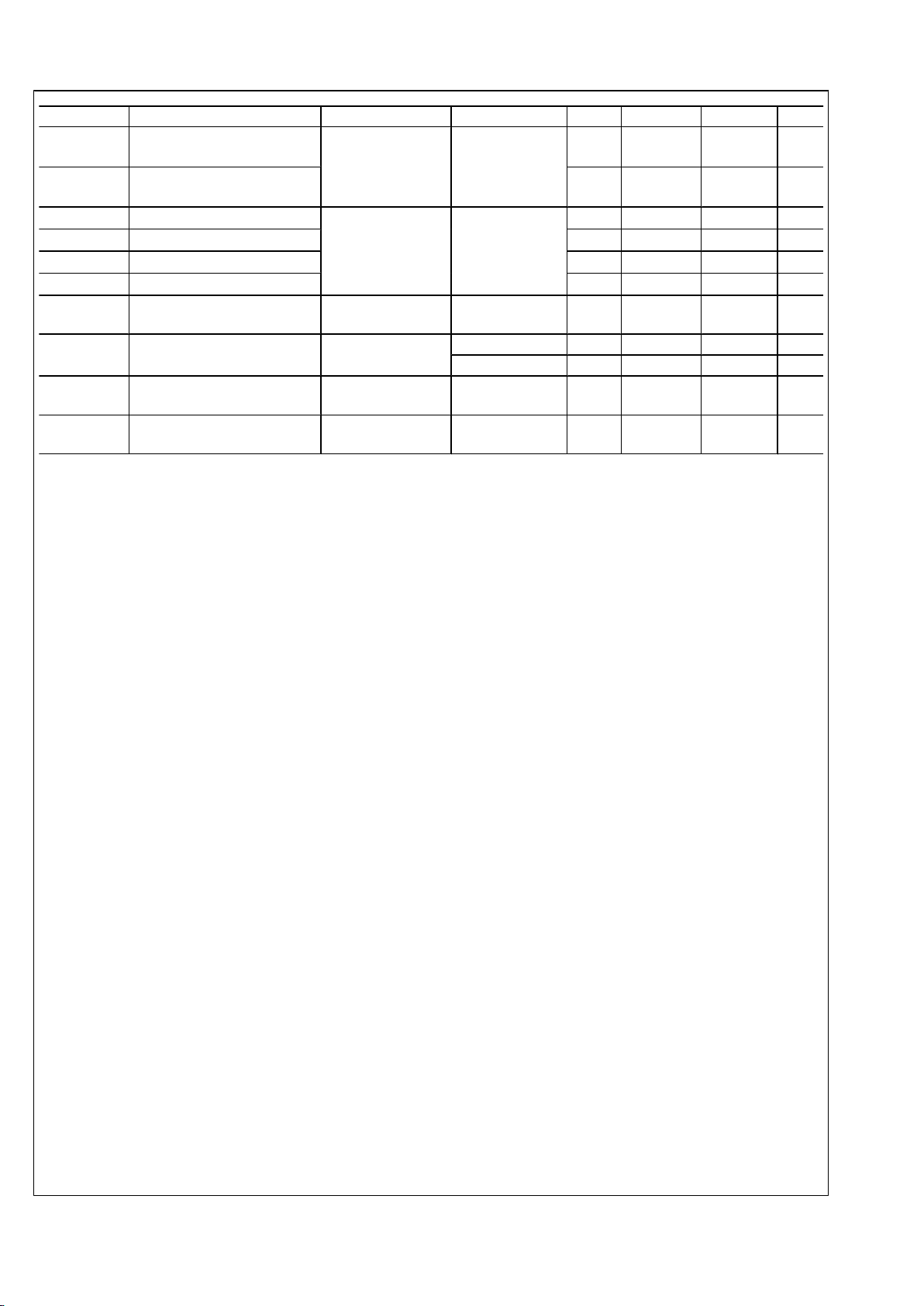
20171902
FIGURE 1. Serializer Input Checker-board Pattern
20171903
FIGURE 2. Deserializer Output Checker-board Pattern
20171904
FIGURE 3. Serializer LVDS Output Load and Transition Times
20171906
FIGURE 4. Serializer Input Clock Transition Times
www.national.com 6
DS90C241/DS90C124
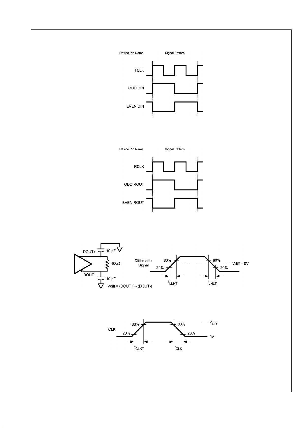
20171907
FIGURE 5. Serializer Setup/Hold Times
20171908
FIGURE 6. Serializer TRI-STATE Test Circuit and Delay
7 www.national.com
DS90C241/DS90C124
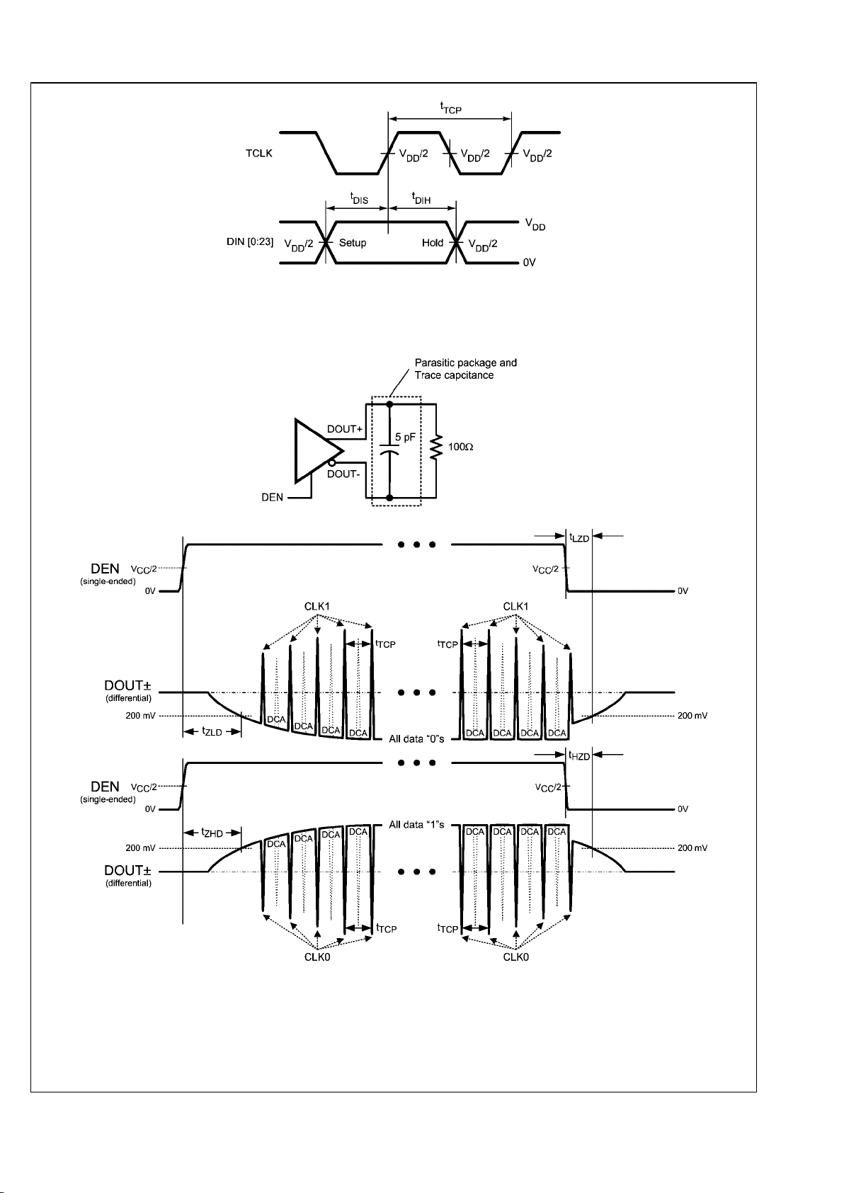
20171909
FIGURE 7. Serializer PLL Lock Time, and TPWDNB TRI-STATE Delays
20171910
FIGURE 8. Serializer Delay
20171915
FIGURE 9. Transmitter Output Eye Opening (TxOUT_E_O)
www.national.com 8
DS90C241/DS90C124
 Loading...