

DS90C032
LVDS Quad CMOS Differential Line Receiver
General Description
The DS90C032 is a quad CMOS differential line receiver designed for applications requiring ultra low power dissipation
and high data rates. The device is designed to support data
rates in excess of 155.5 Mbps (77.7 MHz) utilizing Low Voltage Differential Signaling (LVDS) technology.
The DS90C032 accepts low voltage (350 mV) differential input signals and translates them to CMOS (TTL compatible)
output levels. The receiver supports a TRI-STATE
®
function
that may beusedtomultiplex outputs. The receiver also supports OPEN, shorted and terminated (100Ω) input Fail-safe.
Receiver output will be HIGH for all fail-safe conditions.
The DS90C032 and companion line driver (DS90C031) provide a new alternative to high power psuedo-ECL devices for
high speed point-to-point interface applications.
Features
n
>
155.5 Mbps (77.7 MHz) switching rates
n Accepts small swing (350 mV) differential signal levels
n Ultra low power dissipation
n 600 ps maximum differential skew (5V, 25˚C)
n 6.0 ns maximum propagation delay
n Industrial operating temperature range
n Military operating temperature range option
n Available in surface mount packaging (SOIC) and (LCC)
n Pin compatible with DS26C32A, MB570 (PECL) and
41LF (PECL)
n Supports OPEN, short and terminated input fail-safe
n Compatible with IEEE 1596.3 SCI LVDS standard
n Conforms to ANSI/TIA/EIA-644 LVDS standard
n Available to Standard Microcircuit Drawing (SMD)
5962-95834
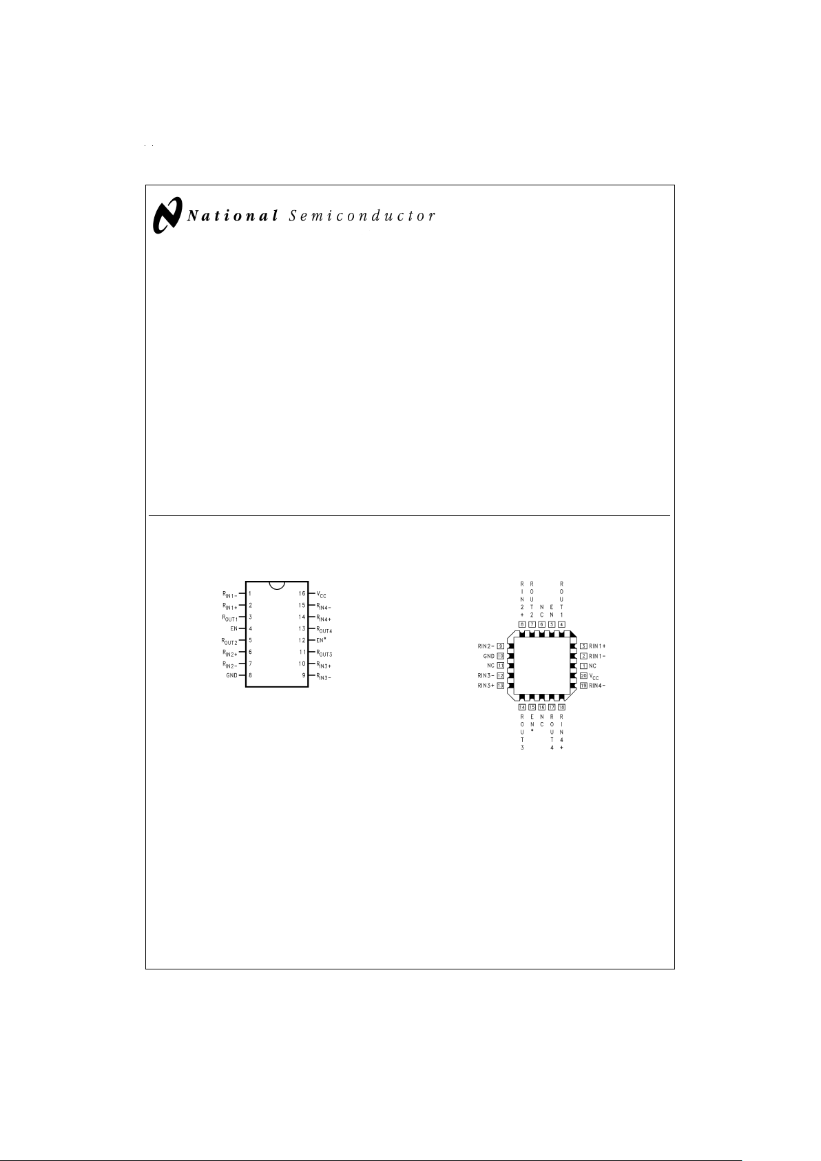
Connection Diagrams
TRI-STATE®is a registered trademark of National Semiconductor Corporation.
Dual-In-Line
DS011945-1
Order Number
DS90C032TM
See NS Package Number M16A
LCC Package
DS011945-20
Order Number
DS90C032E-QML
See NS Package Number E20A
For complete Military Specifications,
refer to appropriate SMD or MDS.
June 1998
DS90C032 LVDS Quad CMOS Differential Line Receiver
© 1998 National Semiconductor Corporation DS011945 www.national.com
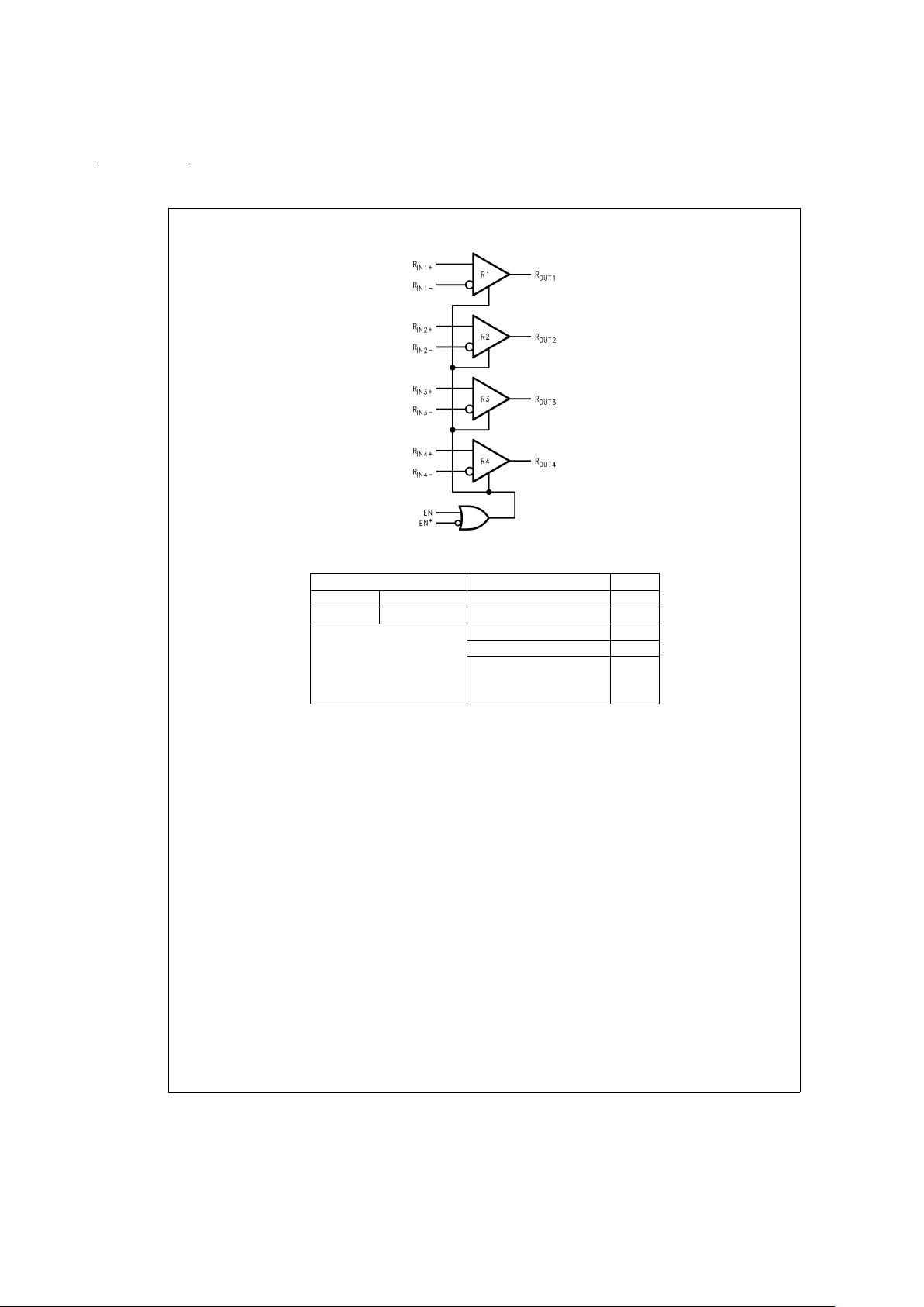
Functional Diagram and Truth Tables
RECEIVER
ENABLES INPUTS OUTPUT
EN EN
*
R
IN+−RIN−
R
OUT
LH X Z
All other combinations V
ID
≥ 0.1V H
of ENABLE inputs V
ID
≤ −0.1V L
Full Fail-safe
OPEN/SHORT
H
or Terminated
DS011945-2
www.national.com 2
Absolute Maximum Ratings (Note 1)
If Military/Aerospace specified devices are required,
please contact the National Semiconductor Sales Office/
Distributors for availability and specifications.
Supply Voltage (V
CC
) −0.3V to +6V
Input Voltage (R
IN+,RIN−
) −0.3V to (VCC+0.3V)
Enable Input Voltage
(EN, EN
*
) −0.3V to (VCC+0.3V)
Output Voltage (R
OUT
) −0.3V to (VCC+0.3V)
Maximum Package Power Dissipation
@
+25˚C
M Package 1025 mW
E Package 1830 mW
Derate M Package 8.2 mW/˚C above +25˚C
Derate E Package 12.2 mW/˚C above +25˚C
Storage Temperature Range −65˚C to +150˚C
Lead Temperature Range
Soldering (4 sec.) +260˚C
Maximum Junction
Temperature (DS90C032T) +150˚C
Maximum Junction
Temperature (DS90C032E) +175˚C
ESD Rating (Note 7)
(HBM, 1.5 kΩ, 100 pF) ≥ 3,500V
(EIAJ, 0 Ω, 200 pF) ≥ 250V
Recommended Operating
Conditions
Min Typ Max Units
Supply Voltage (V
CC
) +4.5 +5.0 +5.5 V
Receiver Input Voltage GND 2.4 V
Operating Free Air Temperature (T
A
)
DS90C032T −40 +25 +85 ˚C
DS90C032E −55 +25 +125 ˚C
Electrical Characteristics
Over Supply Voltage and Operating Temperature ranges, unless otherwise specified. (Note 2)
Symbol Parameter Conditions Pin Min Typ Max Units
V
TH
Differential Input High Threshold V
CM
=
+1.2V R
IN+
,
R
IN−
+100 mV
V
TL
Differential Input Low Threshold −100 mV
I
IN
Input Current V
IN
=
+2.4V V
CC
=
5.5V −10
±
1 +10 µA
V
IN
=
0V −10
±
1 +10 µA
V
OH
Output High Voltage I
OH
=
−0.4 mA, V
ID
=
+200 mV R
OUT
3.8 4.9 V
I
OH
=
−0.4 mA, DS90C032T 3.8 4.9 V
Input terminated
V
OL
Output Low Voltage I
OL
=
2 mA, V
ID
=
−200 mV 0.07 0.3 V
I
OS
Output Short Circuit Current Enabled, V
OUT
=
0V (Note 8) −15 −60 −100 mA
I
OZ
Output TRI-STATE Current Disabled, V
OUT
=
0V or V
CC
−10
±
1 +10 µA
V
IH
Input High Voltage EN,
EN
*
2.0 V
V
IL
Input Low Voltage 0.8 V
I
I
Input Current −10
±
1 +10 µA
V
CL
Input Clamp Voltage I
CL
=
−18 mA −1.5 −0.8 V
I
CC
No Load Supply Current EN, EN
*
=
V
CC
or GND, DS90C032T V
CC
3.5 10 mA
Receivers Enabled Inputs Open DS90C032E 3.5 11 mA
EN, EN
*
=
2.4 or 0.5, Inputs Open 3.7 11 mA
I
CCZ
No Load Supply Current EN=GND, EN
*
=
V
CC
DS90C032T 3.5 10 mA
Receivers Disabled Inputs Open DS90C032E 3.5 11 mA
www.national.com3
Switching Characteristics
V
CC
=
+5.0V, T
A
=
+25˚C DS90C032T (Notes 3, 4, 5, 9)
Symbol Parameter Conditions Min Typ Max Units
t
PHLD
Differential Propagation Delay High to Low C
L
=
5 pF 1.5 3.40 5.0 ns
t
PLHD
Differential Propagation Delay Low to High V
ID
=
200 mV 1.5 3.48 5.0 ns
t
SKD
Differential Skew |t
PHLD−tPLHD
|(
Figure 1
and
Figure 2
) 0 80 600 ps
t
SK1
Channel-to-Channel Skew (Note 5) 0 0.6 1.0 ns
t
TLH
Rise Time 0.5 2.0 ns
t
THL
Fall Time 0.5 2.0 ns
t
PHZ
Disable Time High to Z R
L
=
2kΩ 10 15 ns
t
PLZ
Disable Time Low to Z C
L
=
10 pF 10 15 ns
t
PZH
Enable Time Z to High (
Figure 3
and
Figure 4
) 4 10 ns
t
PZL
Enable Time Z to Low 410ns
Switching Characteristics
V
CC
=
+5.0V
±
10%,T
A
=
−40˚C to +85˚C DS90C032T (Notes 3, 4, 5, 6, 9)
Symbol Parameter Conditions Min Typ Max Units
t
PHLD
Differential Propagation Delay High to Low C
L
=
5 pF 1.0 3.40 6.0 ns
t
PLHD
Differential Propagation Delay Low to High V
ID
=
200 mV 1.0 3.48 6.0 ns
t
SKD
Differential Skew |t
PHLD−tPLHD
|(
Figure 1
and
Figure 2
) 0 0.08 1.2 ns
t
SK1
Channel-to-Channel Skew (Note 5) 0 0.6 1.5 ns
t
SK2
Chip to Chip Skew (Note 6) 5.0 ns
t
TLH
Rise Time 0.5 2.5 ns
t
THL
Fall Time 0.5 2.5 ns
t
PHZ
Disable Time High to Z R
L
=
2kΩ 10 20 ns
t
PLZ
Disable Time Low to Z C
L
=
10 pF 10 20 ns
t
PZH
Enable Time Z to High (
Figure 3
and
Figure 4
) 4 15 ns
t
PZL
Enable Time Z to Low 415ns
Switching Characteristics
V
CC
=
+5.0V
±
10%,T
A
=
−55˚C to +125˚C DS90C032E (Notes 3, 4, 5, 6, 9, 10)
Symbol Parameter Conditions Min Typ Max Units
t
PHLD
Differential Propagation Delay High to Low C
L
=
20 pF 1.0 3.40 8.0 ns
t
PLHD
Differential Propagation Delay Low to High V
ID
=
200 mV 1.0 3.48 8.0 ns
t
SKD
Differential Skew |t
PHLD−tPLHD
|(
Figure 1
and
Figure 2
) 0 0.08 3.0 ns
t
SK1
Channel-to-Channel Skew (Note 5) 0 0.6 3.0 ns
t
SK2
Chip to Chip Skew (Note 6) 7.0 ns
t
PHZ
Disable Time High to Z R
L
=
2kΩ 10 20 ns
t
PLZ
Disable Time Low to Z C
L
=
10 pF 10 20 ns
t
PZH
Enable Time Z to High (
Figure 3
and
Figure 4
) 4 20 ns
t
PZL
Enable Time Z to Low 420ns
www.national.com 4

Parameter Measurement Information
DS011945-3
FIGURE 1. Receiver Propagation Delay and Transition Time Test Circuit
DS011945-4
FIGURE 2. Receiver Propagation Delay and Transition Time Waveforms
DS011945-5
CLincludes load and test jig capacitance.
S
1
=
V
CC
for t
PZL
and t
PLZ
measurements.
S
1
=
GND for t
PZH
and t
PHZ
measurements.
FIGURE 3. Receiver TRI-STATE Delay Test Circuit
DS011945-6
FIGURE 4. Receiver TRI-STATE Delay Waveforms
www.national.com5
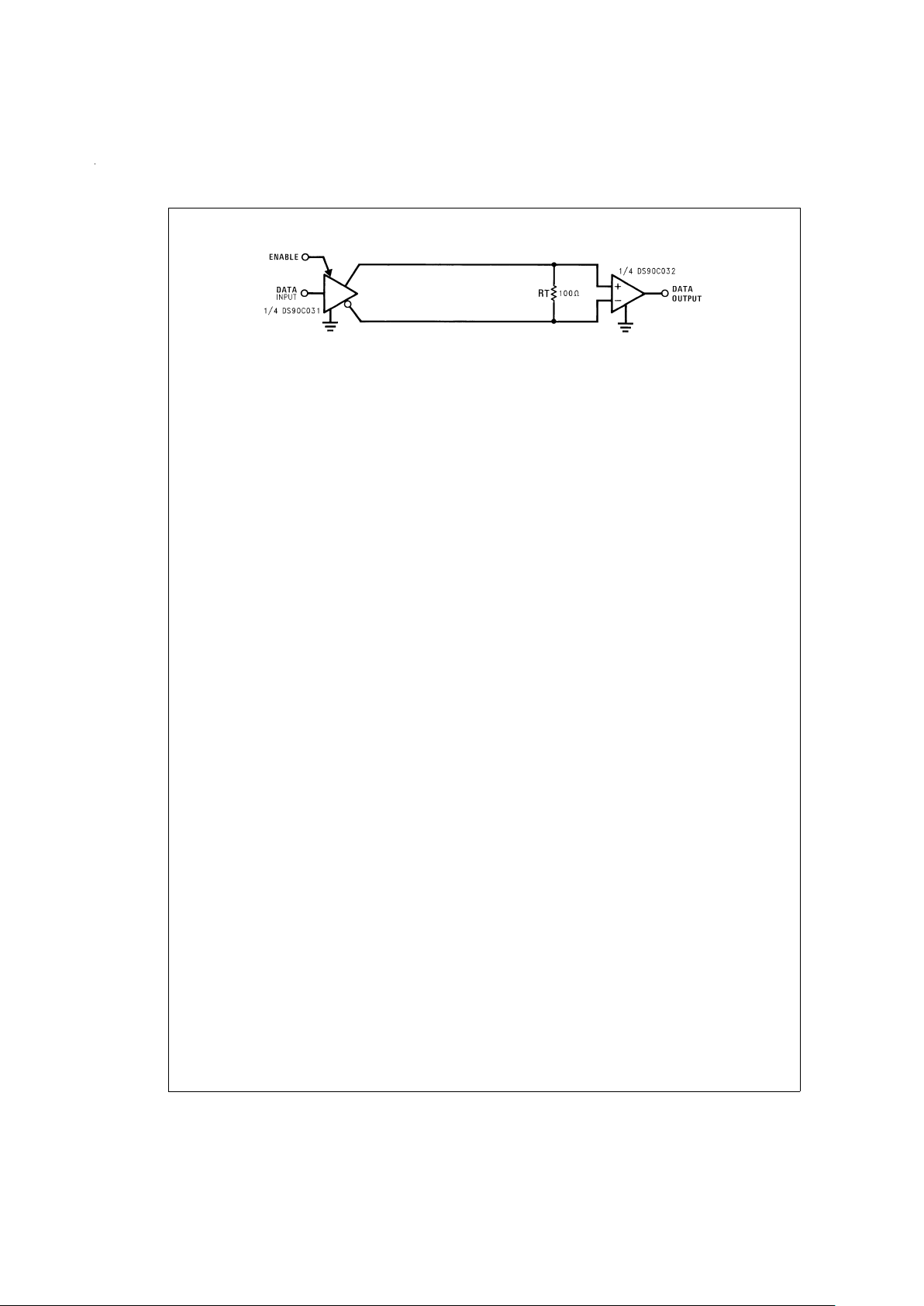
Typical Application
Applications Information
LVDSdrivers and receivers are intended to be primarily used
in an uncomplicated point-to-point configuration as is shown
in
Figure 5.
This configuration provides a clean signaling environment for the quick edge rates of the drivers. The receiver is connected to the driver through a balanced media
which may be a standard twisted pair cable, a parallel pair
cable, or simply PCB traces. Typically the characteristic impedance of the media is in the range of 100Ω. A termination
resistor of 100Ω should be selected to match the media, and
is located as close to the receiver input pins as possible. The
termination resistor converts the current sourced by the
driver into a voltage that is detected by the receiver. Other
configurations are possible such as a multi-receiver configuration, but the effects of a mid-stream connector(s), cable
stub(s), and other impedance discontinuities as well as
ground shifting, noise margin limits, and total termination
loading must be taken into account.
The DS90C032 differential line receiver is capable of detecting signals as low as 100 mV, over a
±
1V common-mode
range centered around +1.2V.This is related to the driver offset voltage which is typically +1.2V.The driven signal is centered around this voltage and may shift
±
1V around this cen-
ter point. The
±
1V shifting may be the result of a ground
potential difference between the driver’s ground reference
and the receiver’s ground reference, the common-mode effects of coupled noise, or a combination of the two. Both receiver input pins should honor their specified operating input
voltage range of 0V to +2.4V (measured from each pin to
ground), exceeding these limits may turn on the ESD protection circuitry which will clamp the bus voltages.
Receiver Fail-Safe:
The LVDS receiver is a high gain, high speed device that
amplifies a small differential signal (20mV) to CMOS logic
levels. Due to the high gain and tight threshold of the receiver,care should be taken to prevent noise from appearing
as a valid signal.
The receiver’s internal fail-safe circuitry is designed to
source/sink a small amount of current, providing fail-safe
protection (a stable known state of HIGH output voltage) for
floating, terminated or shorted receiver inputs.
1. Open Input Pins. The DS90C032 is a quad receiver de-
vice, and if an application requires only 1, 2 or 3 receivers, the unused channel(s) inputs should be left OPEN.
Do not tie unused receiver inputs to ground or any other
voltages. The input is biased by internal high value pull
up and pull down resistors to set the output to a HIGH
state. This internal circuitry will guarantee a HIGH,
stable output state for open inputs.
2. Terminated Input. If the driver is disconnected (cable
unplugged), or if the driver is in a TRI-STATE or
power-off condition, the receiver output will again be in a
HIGH state, even with the end of cable 100Ω termination
resistor across the input pins. The unplugged cable can
become a floating antenna which can pick up noise. If
the cable picks up more than 10mV of differential noise,
the receiver may see the noise as a valid signal and
switch. To insure that any noise is seen as
common-mode and not differential, a balanced interconnect should be used. Twisted pair cable will offer better
balance than flat ribbon cable.
3. Shorted Inputs. If a fault condition occurs that shorts
the receiver inputs together, thus resulting in a 0V differential input voltage, the receiver output will remain in a
HIGH state. Shorted input fail-safe is not supported
across the common-mode range of the device (GND to
2.4V). It is only supported with inputs shorted and no external common-mode voltage applied.
The footprint of the DS90C032 is the same as the industry
standard 26LS32 Quad Differential (RS-422) Receiver.
DS011945-7
FIGURE 5. Point-to-Point Application
www.national.com 6
Pin Descriptions
Pin
No.
(SOIC)
Name Description
2, 6,
10, 14
R
IN+
Non-inverting receiver input pin
1, 7,
9, 15
R
IN−
Inverting receiver input pin
3, 5,
11, 13
R
OUT
Receiver output pin
4 EN Active high enable pin, OR-ed with
EN
*
12 EN*Active low enable pin, OR-ed with EN
16 V
CC
Power supply pin, +5V±10
%
Pin
No.
(SOIC)
Name Description
8 GND Ground pin
Ordering Information
Operating Package Type/ Order Number
Temperature Number
−40˚C to +85˚C SOP/M16A DS90C032TM
−55˚C to +125˚C LCC/E20A DS90C032E-QML
DS90C032E-QML (NSID)
5962-95834 (SMD)
Note 1: “Absolute Maximum Ratings” are those values beyond which the safety of the device cannot be guaranteed. They are not meant to imply that the devices
should be operated at these limits. The table of “Electrical Characteristics” specifies conditions of device operation.
Note 2: Currentinto device pins is defined as positive. Current out of device pins is defined as negative.All voltages are referenced to ground unless otherwise specified.
Note 3: All typicals are given for: V
CC
=
+5.0V, T
A
=
+25˚C.
Note 4: Generator waveform for all tests unless otherwise specified: f=1 MHz, Z
O
=
50Ω,t
r
and tf(0%–100%) ≤ 1 ns for RINand trand tf≤ 6 ns for EN or EN*.
Note 5: Channel-to-Channel Skew is defined as the difference between the propagation delay of one channel and that of the others on the same chip with an event
on the inputs.
Note 6: Chip to Chip Skew is defined as the difference between the minimum and maximum specified differential propagation delays.
Note 7: ESD Rating:
HBM (1.5 kΩ, 100 pF) ≥ 3,500V
EIAJ (0Ω, 200 pF) ≥ 250V
Note 8: Output short circuit current (I
OS
) is specified as magnitude only, minus sign indicates direction only. Only one output should be shorted at a time, do not ex-
ceed maximum junction temperature specification.
Note 9: C
L
includes probe and jig capacitance.
Note 10: For DS90C032E propagation delay measurements are from 0V on the input waveform to the 50%point on the output (R
OUT
).
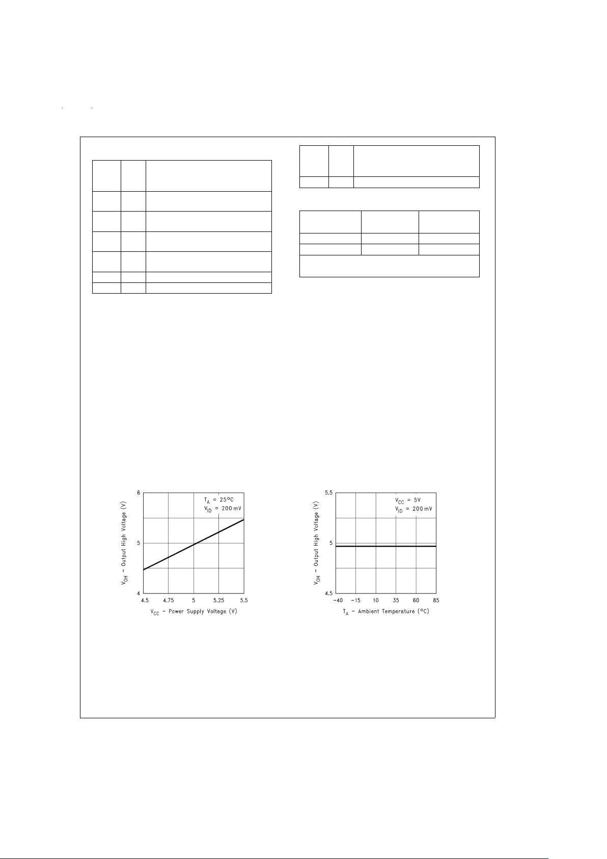
Typical Performance Characteristics
Output High Voltage vs
Power Supply Voltage
DS011945-8
Output High Voltage vs
Ambient Temperature
DS011945-9
www.national.com7

Typical Performance Characteristics (Continued)
Output Low Voltage vs
Power Supply Voltage
DS011945-10
Output Low Voltage vs
Ambient Temperature
DS011945-11
Output Short Circuit Current
vs Power Supply Voltage
DS011945-12
Output Short Circuit Current
vs Ambient Temperature
DS011945-13
Differential Propagation Delay
vs Power Supply Voltage
DS011945-14
Differential Propagation Delay
vs Ambient Temperature
DS011945-15
www.national.com 8

Typical Performance Characteristics (Continued)
Differential Skew vs
Power Supply Voltage
DS011945-16
Differential Skew vs
Ambient Temperature
DS011945-17
Transition Time vs
Power Supply Voltage
DS011945-18
Transition Time vs
Ambient Temperature
DS011945-19
www.national.com9

10
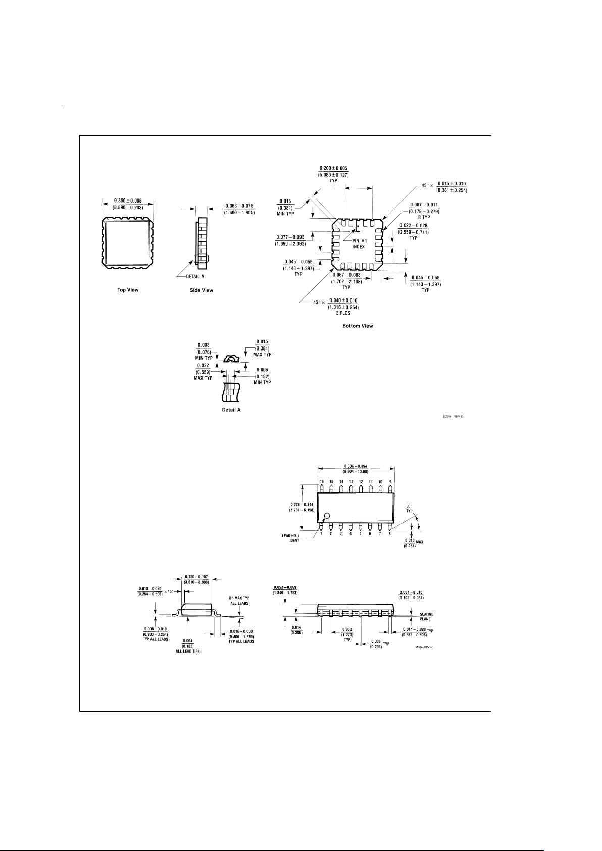
Physical Dimensions inches (millimeters) unless otherwise noted
20-Lead Ceramic Leadless Chip Carrier, Type C
Order Number DS90C032E-QML
NS Package Number E20A
16-Lead (0.150" Wide) Molded Small Outline Package, JEDEC
Order Number DS90C032TM
NS Package Number M16A
www.national.com11

LIFE SUPPORT POLICY
NATIONAL’S PRODUCTS ARE NOT AUTHORIZED FOR USE AS CRITICAL COMPONENTS IN LIFE SUPPORT DEVICES OR SYSTEMS WITHOUT THE EXPRESS WRITTEN APPROVAL OF THE PRESIDENT OF NATIONAL SEMICONDUCTOR CORPORATION. As used herein:
1. Life support devices or systems are devices or systems which, (a) are intended for surgical implant into
the body, or (b) support or sustain life, and whose failure to perform when properly used in accordance
with instructions for use provided in the labeling, can
be reasonably expected to result in a significant injury
to the user.
2. A critical component in any component of a life support
device or system whose failure to perform can be reasonably expected to cause the failure of the life support
device or system, or to affect its safety or effectiveness.
National Semiconductor
Corporation
Americas
Tel: 1-800-272-9959
Fax: 1-800-737-7018
Email: support@nsc.com
www.national.com
National Semiconductor
Europe
Fax: +49 (0) 1 80-530 85 86
Email: europe.support@nsc.com
Deutsch Tel: +49 (0) 1 80-530 85 85
English Tel: +49 (0) 1 80-532 78 32
Français Tel: +49 (0) 1 80-532 93 58
Italiano Tel: +49 (0) 1 80-534 16 80
National Semiconductor
Asia Pacific Customer
Response Group
Tel: 65-2544466
Fax: 65-2504466
Email: sea.support@nsc.com
National Semiconductor
Japan Ltd.
Tel: 81-3-5620-6175
Fax: 81-3-5620-6179
DS90C032 LVDS Quad CMOS Differential Line Receiver
National does not assume any responsibility for use of any circuitry described, no circuit patent licenses are implied and National reserves the right at any time without notice to change said circuitry and specifications.
 Loading...