

NSC DS78C20J-883, DS88C20N Datasheet
DS78C20/DS88C20
Dual CMOS Compatible Differential Line Receiver
DS78C20/DS88C20 Dual CMOS Compatible Differential Line Receiver
May 1998
General Description
The DS78C20 and DS88C20 are high performance, dual differential, CMOS compatible line receivers for both balanced
and unbalanced digital data transmission. The inputs are
compatible with EIA and Federal Standards.
Input specifications meet or exceed those of the popular
DS7820/DS8820 line receiver, and the pinout is identical.
A response pin is provided for controlling sensitivity to input
noise spikes with an external capacitor. Each receiver includes a 180Ω terminating resistor, which may be used optionally on twisted pair lines. The DS78C20 is specified over
a −55˚C to +125˚C operating temperature range, and the
DS88C20 over a 0˚C to +70˚C range.
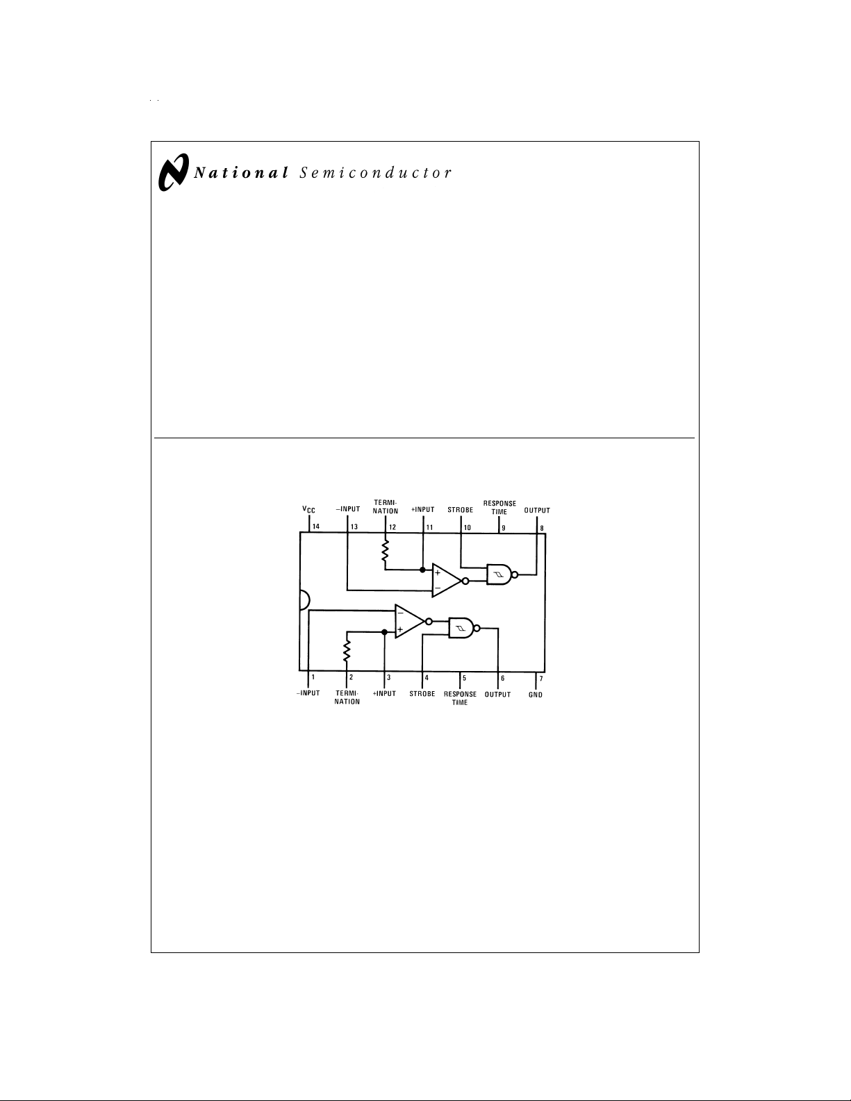
Connection Diagram
Dual-In-Line Package
Features
n Meets requirements of EIA Standards RS-232-C RS-422
and RS-423, and Federal Standards 1020 and 1030
n Input voltage range of
common-mode)
n Separate strobe input for each receiver
1
n
⁄2VCCstrobe threshold for CMOS compatibility
n 5k typical input impedance
n 50 mV input hysteresis
n 200 mV input threshold
n Operation voltage range=4.5V to 15V
n DS7830/DS8830 recommended driver
±
15V (differential or
DS005798-1
Top View
Order Number DS88C20N
See NS Package Numbers N14A
For Complete Military Product Specifications,
refer to the appropriate SMD or MDS.
Order Number DS78C20J/883
See NS Package Number J14A
© 1998 National Semiconductor Corporation DS005798 www.national.com

Absolute Maximum Ratings (Note 2)
If Military/Aerospace specified devices are required,
please contact the National Semiconductor Sales Office/
Distributors for availability and specifications.
Supply Voltage 18V
Common-Mode Voltage
Differential Input Voltage
Strobe Voltage 18V
Output Sink Current 50 mA
Maximum Power Dissipation (Note 1) at 25˚C
Cavity Package 1364 mW
±
25V
±
25V
Lead Temperature (Soldering, 4 seconds) 260˚C
Operating Conditions
Supply Voltage (V
Temperature (T
) 4.5 15 V
CC
)
A
DS78C20 −55 +125 ˚C
DS88C20 0 +70 ˚C
Common-Mode Voltage (V
Note 1: Derate cavity package 9.1 mW/˚C; derate molded package 10.2
mW/˚C above 25˚C.
Min Max Units
) −15 +15 V
CM
Molded Package 1280 mW
Storage Temperature Range −65˚C to
+150˚C
Electrical Characteristics (Notes 3, 4)
Symbol Parameter Conditions Min Typ Max Units
V
R
R
I
V
V
V
I
I
I
V
V
I
Differential Threshold I
TH
Voltage V
Input Resistance −15V ≤ VCM≤ 15V 5 kΩ
IN
Line Termination
T
Resistance
Data Input Current V
IND
(Unterminated) V
Input Balance I
THB
Logical “1” Output Voltage I
OH
Logical “0” Output Voltage I
OL
Power Supply Current 15V ≤ VCM≤ −15V, V
CC
Logical “1” Strobe Input
IN(1)
Current
Logical “0” Strobe Input
IN(0)
Current
Logical “1” Strobe Input I
IH
Voltage V
Logical “0” Strobe Input I
IL
Voltage V
Output Short-Circuit
OS
Current
=
−200 µA, −10V ≤ V
OUT
≥ VCC−1.2V −15V ≤ VCM≤ 15V 0.06 0.3 V
OUT
=
I
OUT
1.6 mA, V
≤ 0.5V −10V ≤ VCM≤ 10V −0.08 −0.2 V
OUT
−15V ≤ V
=
T
25˚C 100 180 300 Ω
A
=
10V 2 3.1 mA
CM
=
0V 0 −0.5 mA
CM
=
V
−10V −2 −3.1 mA
CM
OUT
V
CC
=
200 µA, V
−1.2V, R
≥ −7V ≤ VCM≤ 7V
OUT
=
500Ω, 0.1 0.4 V
S
≤ 10V 0.06 0.2 V
CM
≤ 15V −0.08 −0.3 V
CM
(Note 6)
=
I
1.6 mA, V
OUT
=
R
500Ω, (Note 6)
S
=
−200 µA, V
OUT
=
1.6 mA, V
OUT
=
V
−0.5V V
DIFF
≤ 0.5V, −7V ≤ VCM≤ 7V −0.1 −0.4 V
OUT
=
1V V
DIFF
=
−1V 0.25 0.5 V
DIFF
=
5.5V 8 15 mA
CC
=
15V 15 30 mA
CC
−1.2 VCC−0.75 V
CC
(Both Receivers)
=
V
STROBE
V
STROBE
OUT
OUT
OH
V
15V, V
=
0V, V
=
1.6 mA, V
=
−200 µA, V
=
−1.2V V
V
CC
=
0V, V
OUT
DIFF
OL
=
CC
=
3V V
DIFF
=
−3V V
≤ 0.5V V
15V, V
STROBE
=
15V 15 100 µA
CC
=
15V −0.5 −100 µA
CC
=
5V 3.5 2.5 V
CC
=
10V 8.0 5.0 V
CC
=
V
15V 12.5 7.5 V
CC
=
5V 2.5 1.5 V
CC
=
10V 5.0 2.0 V
CC
=
V
15V 7.5 2.5 V
CC
=
0V, (Note 5) −5 −20 −40 mA
www.national.com 2
 Loading...