NSC DP8571AN Datasheet
DP8571A Timer Clock Peripheral (TCP)
General Description
The DP8571A is intended for use in microprocessor based
systems where information is required for multi-tasking, data
logging or general time of day/date information. This device
is implemented in low voltage silicon gate microCMOS technology to provide low standby power in battery back-up environments. The circuit’s architecture is such that it looks
like a contiguous block of memory or I/O ports. The address
space is organized as 2 software selectable pages of 32
bytes. This includes the Control Registers, the Clock Counters, the Alarm Compare RAM, the Timers and their data
RAM, and the Time Save RAM. Any of the RAM locations
that are not being used for their intended purpose may be
used as general purpose CMOS RAM.
Time and date are maintained from 1/100 of a second to
year and leap year in a BCD format, 12 or 24 hour modes.
Day of week, day of month and day of year counters are
provided. Time is controlled by an on-chip crystal oscillator
requiring only the addition of the crystal and two capacitors.
The choice of crystal frequency is program selectable.
Two independent multifunction 10 MHz 16-bit timers are
provided. These timers operate in four modes. Each has its
own prescaler and can select any of 7 possible clock inputs.
Thus, by programming the input clocks and the timer counter values a very wide range of timing durations can be
achieved. The range is from about 400 ns (4.915 MHz oscillator) to 65,535 seconds (18 hrs., 12 min.).
Power failure logic and control functions have been integrated on chip. This logic is used by the TCP to issue a power fail
interrupt, and lock out the mp interface. The time power fails
may be logged into RAM automatically when V
Additionally, two supply pins are provided. When V
l
VCC, internal circuitry will automatically switch from the
main supply to the battery supply. Status bits are provided
to indicate initial application of battery power, system power,
and low battery detect. (Continued)
Features
Y
Full function real time clock/calendar
Ð 12/24 hour mode timekeeping
Ð Day of week and day of years counters
Ð Four selectable oscillator frequencies
Ð Parallel resonant oscillator
Y
Two 16-bit timers
Ð 10 MHz external clock frequency
Ð Programmable multi-function output
Ð Flexible re-trigger facilities
Y
Power fail features
Ð Internal power supply switch to external battery
Ð Power Supply Bus glitch protection
Ð Automatic log of time into RAM at power failure
Y
On-chip interrupt structure
Ð Periodic, alarm, timer and power fail interrupts
Y
Up to 44 bytes of CMOS RAM
Y
INTR/MFO pins programmable High/Low and push-pull
or open drain
May 1993
l
BB
DP8571A Timer Clock Peripheral (TCP)
VCC.
BB
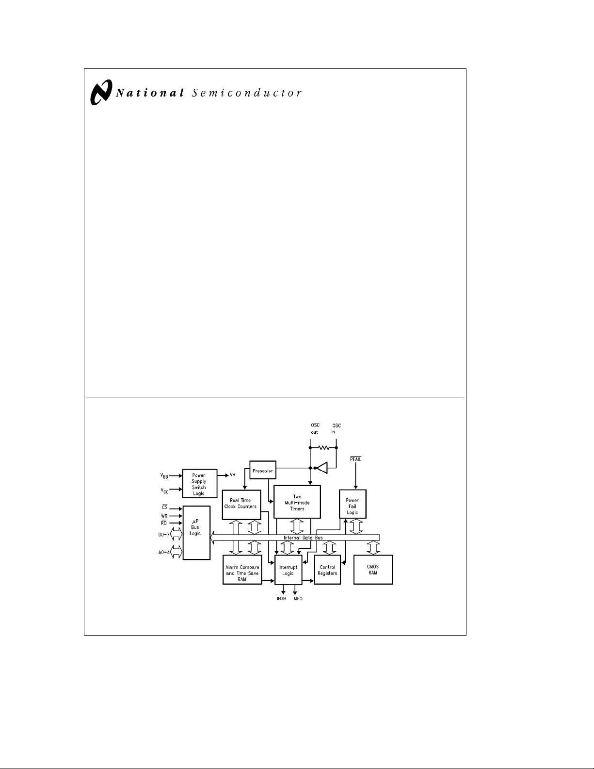
Block Diagram
FIGURE 1
TRI-STATEÉis a registered trademark of National Semiconductor Corporation.
C
1995 National Semiconductor Corporation RRD-B30M75/Printed in U. S. A.
TL/F/9979
TL/F/9979– 1

Absolute Maximum Ratings (Notes1&2)
If Military/Aerospace specified devices are required,
please contact the National Semiconductor Sales
Office/Distributors for availability and specifications.
Supply Voltage (V
CC
)
DC Input Voltage (VIN)
DC Output Voltage (V
OUT
)
Storage Temperature Range
Power Dissipation (PD) 500 mW
Lead Temperature (Soldering, 10 sec.) 260§C
b
0.5V toa7.0V
b
0.5V to V
b
0.5V to V
b
65§Ctoa150§C
CC
CC
a
0.5V
a
0.5V
Operation Conditions
)
Socket
Socket 85
b40a
Min Max Unit
b
0.4 V
CC
0.0 V
CC
85§C
§
Supply Voltage (V
) (Note 3) 4.5 5.5 V
CC
Supply Voltage (VBB) (Note 3) 2.2 V
DC Input or Output Voltage
(V
Operation Temperature (T
IN,VOUT
)
A
Electr-Static Discharge Rating TBD 1 kV
Transistor Count 15,200
Typical Values
i
DIP Board
JA
i
PLCC Board 77§C/W
JA
DC Electrical Characteristics
V
CC
e
5Vg10%, V
BB
e
3V, V
Symbol Parameter Conditions Min Max Units
V
IH
V
IL
V
OH
V
OL
I
IN
I
OZ
I
LKG
I
CC
I
CC
I
BB
I
BLK
Note 1: Absolute Maximum Ratings are those values beyond which damage to the device may occur.
Note 2: Unless otherwise specified all voltages are referenced to ground.
Note 3: For F
2.2V min. In single Supply Mode (Power connected to V
Note 4: This parameter (V
Note 5: This specification tests I
Note 6: This specification tests I
Note 7: This specification is tested with both the timers and OSC IN driven by a signal generator. Contents of the Test Register
configured as buffered oscillator out and MFO, INTR, are configured as open drain.
Note 8: This specification is tested with both the timers off, and only OSC IN is driven by a signal generator. Contents of the Test Register
pin is not configured as buffered oscillator out.
High Level Input Voltage Any Inputs Except OSC IN, 2.0 V
(Note 4) OSC IN with External Clock V
Low Level Input Voltage All Inputs Except OSC IN 0.8 V
High Level Output Voltage I
(Excluding OSC OUT) I
Low Level Output Voltage I
(Excluding OSC OUT) I
Input Current (Except OSC IN) V
Output TRI-STATEÉCurrent V
Output High Leakage Current V
T1, MFO, INTR Pins Outputs Open Drain
Quiescent Supply Current F
(Note 7) V
Quiescent Supply Current V
(Single Supply Mode) V
(Note 7) F
Standby Mode Battery V
Supply Current OSC OUT
(Note 8) other pins
Battery, Supply Leakage 2.2VsV
e
4.194304 or 4.9152 MHz, VBBminimume2.8V. In battery backed mode, V
OSC
) is not tested on all pins at the same time.
IH
with all power fail circuitry disabled, by setting D7 of Interrupt Control Register 1 to 0.
CC
with all power fail circuitry enabled, by setting D7 of Interrupt Control Register 1 to 1.
CC
PFAIL
l
VIH,C
CC
e
100 pF (unless otherwise specified)
L
b
0.1 V
BB
OSC IN with External Clock 0.1 V
OUT
OUT
OUT
OUT
V
V
F
V
V
F
F
F
other pins at GND
V
V
pin) 4.5VsV
eb
20 mAV
eb
4.0 mA 3.5 V
e
20 mA 0.1 V
e
4.0 mA 0.25 V
e
VCCor GND
IN
e
VCCor GND
OUT
e
VCCor GND
OUT
e
32.768 kHz
OSC
e
VCCor GND (Note 5)
IN
e
VCCor GND (Note 6)
IN
e
VIHor VIL(Note 6)
IN
e
4.194304 MHz or
OSC
4.9152 MHz 8 mA
e
VCCor GND (Note 6) 20 mA
IN
e
VIHor VIL(Note 6)
IN
e
GND
BB
e
VCCor GND
IN
e
32.768 kHz 80 mA
OSC
e
4.9152 MHz or 7.5 mA
OSC
4.194304 MHz
e
GND
CC
e
open circuit,
e
GND
e
32.768 kHz 10 mA
OSC
e
4.9152 MHz or 400 mA
OSC
4.194304 MHz
s
4.0V
BB
CC
CC
e
e
CC
GND, V
5.5V, V
s
5.5V.
e
4.0V 1.5 mA
BB
e
2.2V
BB
s
b
V
BB
CC
b
0.1 V
CC
b
5 mA
0.4V. Single Supply Mode: Data retention voltage is
e
00(H), the MFO pin is not
g
1.0 mA
g
5.0 mA
g
5.0 mA
260 mA
1.0 mA
12.0 mA
e
00(H) and the MFO
V
C/W
2
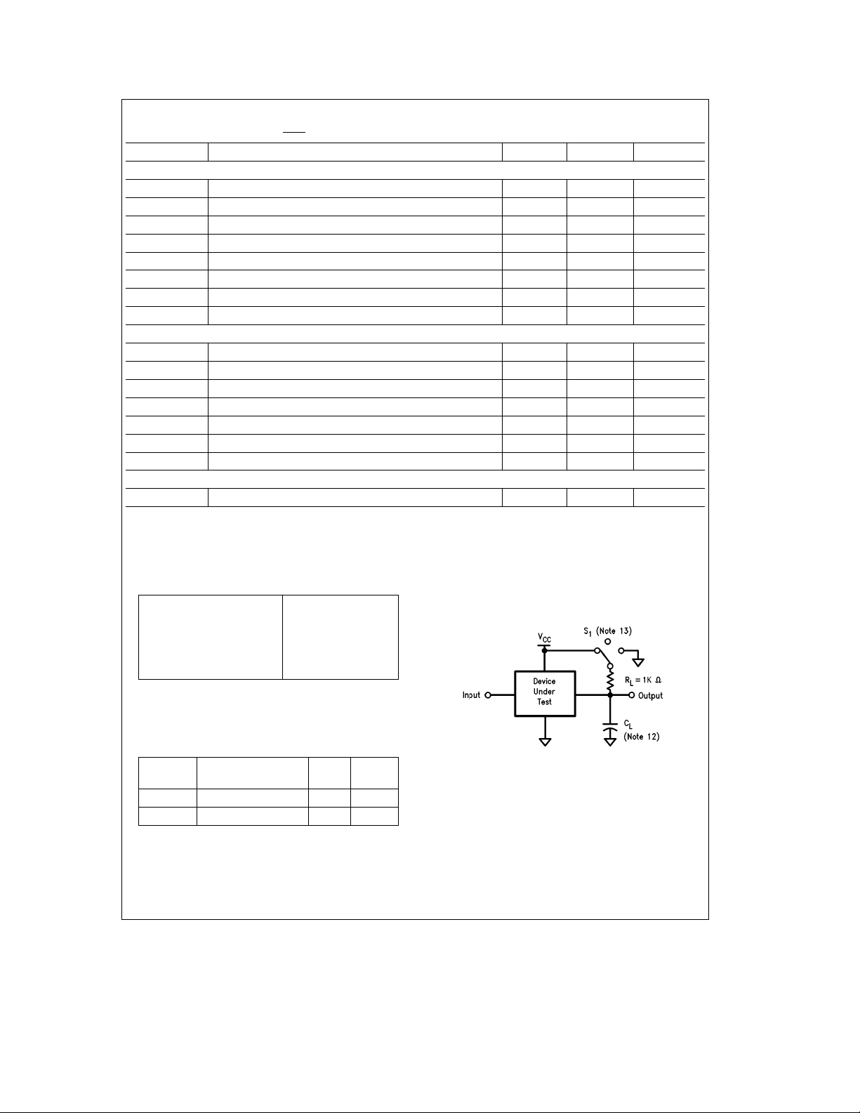
AC Electrical Characteristics
V
CC
e
5Vg10%, V
BB
e
3V, V
PFAIL
l
VIH,C
e
100 pF (unless otherwise specified)
L
Symbol Parameter Min Max Units
READ TIMING
t
AR
t
RW
t
CD
t
RAH
t
RD
t
DZ
t
RCH
t
DS
Address Valid Prior to Read Strobe 20 ns
Read Strobe Width (Note 9) 80 ns
Chip Select to Data Valid Time 80 ns
Address Hold after Read (Note 10) 3 ns
Read Strobe to Valid Data 70 ns
Read or Chip Select to TRI-STATE 60 ns
Chip Select Hold after Read Strobe 0 ns
Minimum Inactive Time between Read or Write Accesses 50 ns
WRITE TIMING
t
AW
t
WAH
t
CW
t
WW
t
DW
t
WDH
t
WCH
Address Valid before Write Strobe 20 ns
Address Hold after Write Strobe (Note 10) 3 ns
Chip Select to End of Write Strobe 90 ns
Write Strobe Width (Note 11) 80 ns
Data Valid to End of Write Strobe 50 ns
Data Hold after Write Strobe (Note 10) 3 ns
Chip Select Hold after Write Strobe 0 ns
INTERRUPT TIMING
t
ROLL
Note 9: Read Strobe width as used in the read timing table is defined as the period when both chip select and read inputs are low. Hence read commences when
both signals are low and terminates when either signal returns high.
Note 10: Hold time is guaranteed by design but not production tested. This limit is not used to calculate outgoing quality levels.
Note 11: Write Strobe width as used in the write timing table is defined as the period when both chip select and write inputs are low. Hence write commences when
both signals are low and terminates when either signal returns high.
Clock rollover to INTR out is typically 16.5 ms
AC Test Conditions
Input Pulse Levels GND to 3.0V
Input Rise and Fall Times 6 ns (10% –90%)
Input and Output
Reference Levels
TRI-STATE Reference Active High
Levels (Note 13) Active Low
Note 12: C
Note 13: S1
Capacitance (T
Note 14: This parameter is not 100% tested.
Note 15: Output rise and fall times 25 ns max (10% –90%) with 100 pF load.
e
100 pF, includes jig and scope capacitance.
L
e
VCCfor active low to high impedance measurements.
e
GND for active high to high impedance measurements.
S1
e
open for all other timing measurements.
S1
e
25§C, fe1 MHz)
A
Symbol
C
IN
C
OUT
Parameter
(Note 14)
Input Capacitance 5 pF
Output Capacitance 7 pF
1.3V
a
0.5V
b
0.5V
Typ Units
TL/F/9979– 2
3
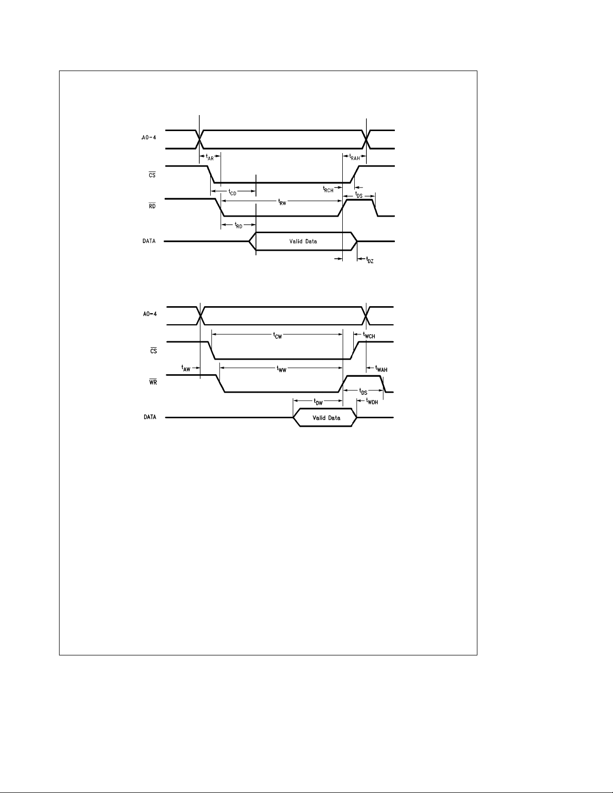
Timing Waveforms
Read Timing Diagram
TL/F/9979– 3
Write Timing Diagram
TL/F/9979– 4
4
General Description (Continued)
The DP8571A’s interrupt structure provides four basic types
of interrupts: Periodic, Alarm/Compare, Timer, and Power
Fail. Interrupt mask and status registers enable the masking
and easy determination of each interrupt.
One dedicated general purpose interrupt output is provided.
A second interrupt output is available on the Multiple Function Output (MFO) pin. Each of these may be selected to
generate an interrupt from any source. Additionally, the
MFO pin may be programmed to be either as oscillator output or Timer 0’s output.
Pin Description
CS,RD,WR(Inputs): These pins interface to mP control
lines. The CS
write operations. Read and Write pins are also active low
and enable reading or writing to the TCP. All three pins are
disabled when power failure is detected. However, if a read
or write is in progress at this time, it will be allowed to complete its cycle.
A0–A4 (Inputs): These 5 pins are for register selection.
They individually control which location is to be accessed.
These inputs are disabled when power failure is detected.
OSC IN (Input): OSC OUT (Output): These two pins are
used to connect the crystal to the internal parallel resonant
oscillator. The oscillator is always running when power is
applied to V
the Real Time Mode Register have been set.
MFO (Output): The multi-function output can be used as a
second interrupt output for interrupting the mP. This pin can
also provide an output for the oscillator or the internal Timer
0. The MFO output can be programmed active high or low,
open drain or push-pull. If in battery backed mode and a
pull-up resistor is attached, it should be connected to a voltage no greater than V
during battery operation (V
INTR (Output): The interrupt output is used to interrupt the
processor when a timing event or power fail has occurred
and the respective interrupt has been enabled. The INTR
output can be programmed active high or low, push-pull or
open drain. If in battery backed mode and a pull-up resistor
is attached, it should be connected to a voltage no greater
than V
operation (V
clear the INTR, writea1totheappropriate bit(s) in the Main
Status Register.
D0–D7 (Input/Output): These 8 bidirectional pins connect
to the host mP’s data bus and are used to read from and
write to the TCP. When the PFAIL
is not in progress, these pins are at TRI-STATE.
pin is an active low enable for the read and
and VCC, and the correct crystal select bits in
BB
. This pin is configured open drain
BB
l
VCC).
BB
. This pin is configured open drain during battery
BB
l
VCC). The output is a DC voltage level. To
BB
pin goes low and a write
PFAIL
(Input): In battery backed mode, this pin can have a
digital signal applied to it via some external power detection
logic. When PFAIL
e
logic 0 the TCP goes into a lockout
mode, in a minimum of 30 ms or a maximum of 63 ms unless
lockout delay is programmed. In the single power supply
mode, this pin is not useable as an input and should be tied
to V
. Refer to section on Power Fail Functional Descrip-
CC
tion.
V
(Battery Power Pin): This pin is connected to a back-
BB
up power supply. This power supply is switched to the internal circuitry when the V
ing this pin eliminates the need for external logic to switch in
becomes lower than VBB. Utiliz-
CC
and out the back-up power supply. If this feature is not to be
used then this pin must be tied to ground, the TCP programmed for single power supply only, and power applied to
the V
pin.
CC
VCC: This is the main system power pin.
GND: This is the common ground power pin for both V
and VCC.
BB
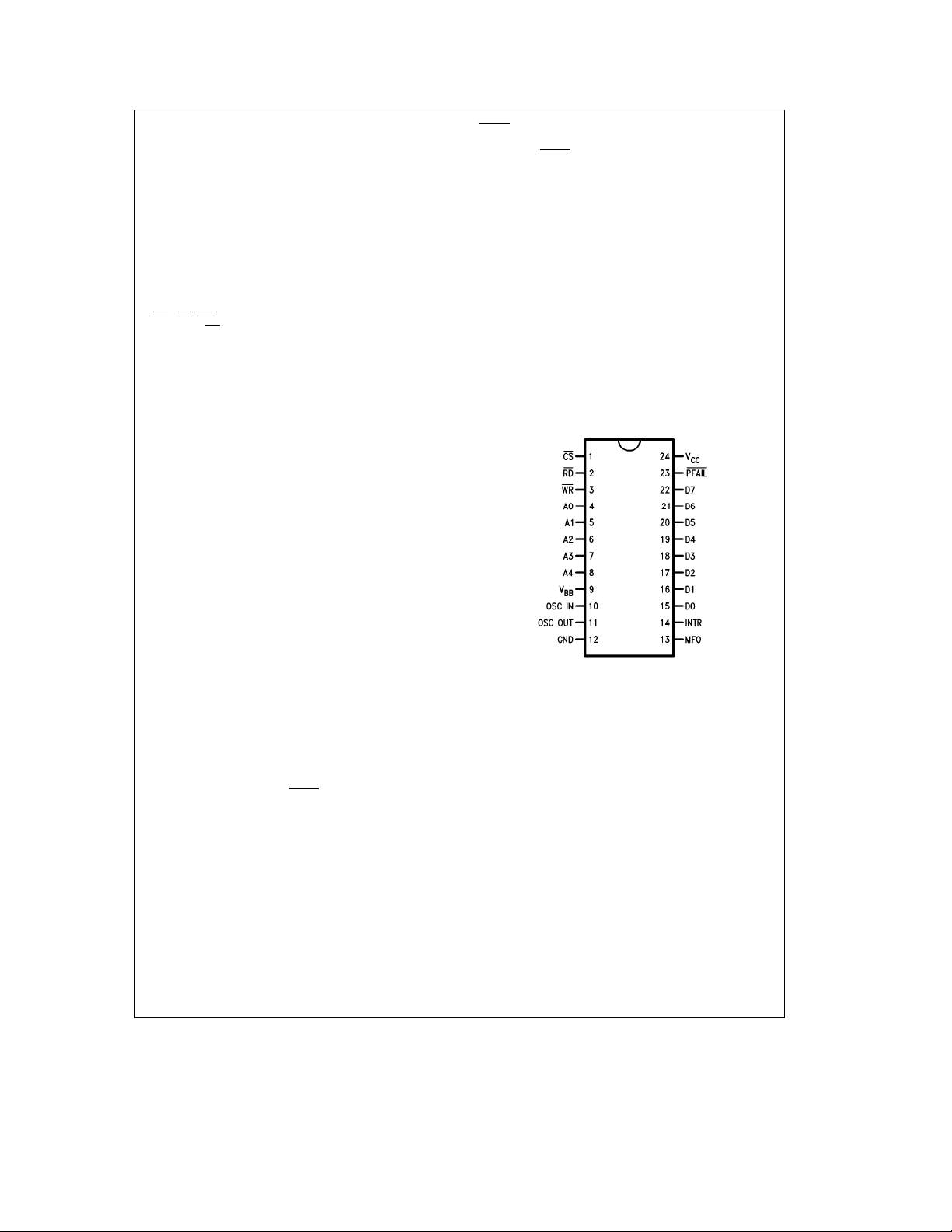
Connection Diagram
Dual-In-Line
Top View
Order Number DP8571AN
See NS Package Number N24C
TL/F/9979– 5
5
Functional Description
The DP8571A contains a fast access real time clock, two 10
MHz 16-bit timers, interrupt control logic, power fail detect
logic, and CMOS RAM. All functions of the TCP are controlled by a set of nine registers. A simplified block diagram
that shows the major functional blocks is given in
The blocks are described in the following sections:
1. Real Time Clock
2. Oscillator Prescaler
3. Interrupt Logic
4. Power Failure Logic
5. Additional Supply Management
6. Timers
Figure 1
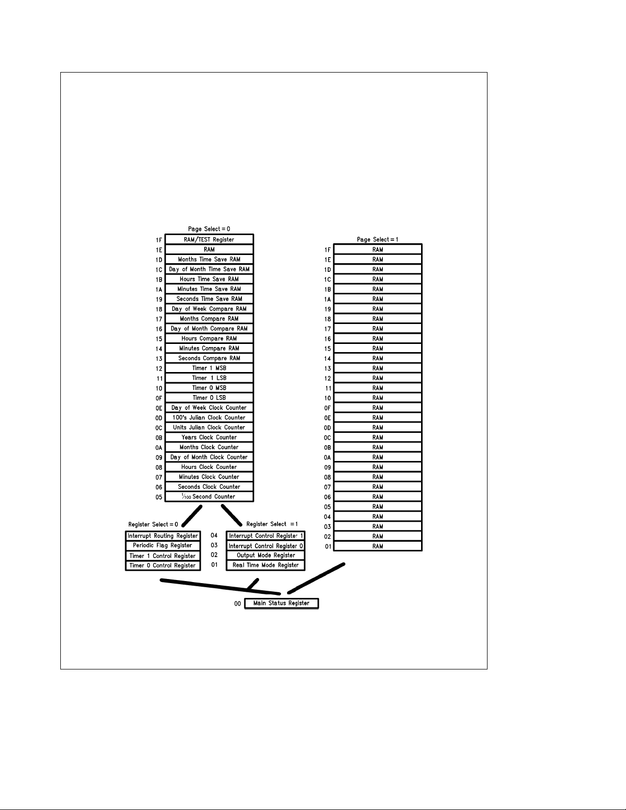
The memory map of the TCP is shown in the memory addressing table. The memory map consists of two 31 byte
pages with a main status register that is common to both
pages. A control bit in the Main Status Register is used to
select either page.
.
Page 0 contains all the clock timer functions, while page 1
has scratch pad RAM. The control registers are split into
two separate blocks to allow page 1 to be used entirely as
scratch pad RAM. Again a control bit in the Main Status
Register is used to select either control register block.
Figure 2
shows the basic concept.
FIGURE 2. DP8571A Internal Memory Map
6
TL/F/9979– 6
Functional Description (Continued)
INITIAL POWER-ON of BOTH V
VBBand VCCmay be applied in any sequence. In order for
the power fail circuitry to function correctly, whenever power
is off, the V
maximum of 1 MX. The user should be aware that the con-
pin must see a path to ground through a
CC
trol registers will contain random data. The first task to be
carried out in an initialization routine is to start the oscillator
by writing to the crystal select bits in the Real Time Mode
Register. If the DP8571A is configured for single supply
mode, an extra 50 mA may be consumed until the crystal
select bits are programmed. The user should also ensure
that the TCP is not in test mode (see register descriptions).
REAL TIME CLOCK FUNCTIONAL DESCRIPTION
As shown in
Figure 2
, the clock has 10 bytes of counters,
which count from 1/100 of a second to years. Each counter
counts in BCD and is synchronously clocked. The count sequence of the individual byte counters within the clock is
shown later in Table VII. Note that the day of week, day of
month, day of year, and month counters all roll over to 1.
The hours counter in 12 hour mode rolls over to 1 and the
AM/PM bit toggles when the hours rolls over to 12
e
(AM
0, PMe1). The AM/PM bit is bit D7 in the hours
counter.
All other counters roll over to 0. Also note that the day of
year counter is 12 bits long and occupies two addresses.
Upon initial application of power the counters will contain
random information.
READING THE CLOCK: VALIDATED READ
Since clocking of the counter occurs asynchronously to
reading of the counter, it is possible to read the counter
while it is being incremented (rollover). This may result in an
incorrect time reading. Thus to ensure a correct reading of
the entire contents of the clock (or that part of interest), it
must be read without a clock rollover occurring. In general
this can be done by checking a rollover bit. On this chip the
periodic interrupt status bits can serve this function. The
following program steps can be used to accomplish this.
1. Initialize program for reading clock.
2. Dummy read of periodic status bit to clear it.
3. Read counter bytes and store.
4. Read rollover bit, and test it.
5. If rollover occured go to 3.
6. If no rollover, done.
To detect the rollover, individual periodic status bits can be
polled. The periodic bit chosen should be equal to the highest frequency counter register to be read. That is if only
SECONDS through HOURS counters are read, then the
SECONDS periodic bit should be used.
READING THE CLOCK: INTERRUPT DRIVEN
Enabling the periodic interrupt mask bits cause interrupts
just as the clock rolls over. Enabling the desired update rate
and providing an interrupt service routine that executes in
less than 10 ms enables clock reading without checking for
a rollover.
READING THE CLOCK: LATCHED READ
Another method to read the clock that does not require
checking the rollover bit is to write a one into the Time
BB
and V
CC
Save Enable bit (D7) of the Interrupt Routing Register, and
then to write a zero. Writing a one into this bit will enable the
clock contents to be duplicated in the Time Save RAM.
Changing the bit from a one to a zero will freeze and store
the contents of the clock in Time Save RAM. The time then
can be read without concern for clock rollover, since internal logic takes care of synchronization of the clock. Because only the bits used by the clock counters will be
latched, the Time Save RAM should be cleared prior to use
to ensure that random data stored in the unused bits do not
confuse the host microprocessor. This bit can also provide
time save at power failure, see the Additional Supply Management Functions section. With the Time Save Enable bit
at a logical 0, the Time Save RAM may be used as RAM if
the latched read function is not necessary.
INITIALIZING AND WRITING TO THE
CALENDAR-CLOCK
Upon initial application of power to the TCP or when making
time corrections, the time must be written into the clock. To
correctly write the time to the counters, the clock would
normally be stopped by writing the Start/Stop
bit in the Real
Time Mode Register to a zero. This stops the clock from
counting and disables the carry circuitry. When initializing
the clock’s Real Time Mode Register, it is recommended
that first the various mode bits be written while maintaining
the Start/Stop
second time with the Start/Stop
bit reset, and then writing to the register a
bit set.
The above method is useful when the entire clock is being
corrected. If one location is being updated the clock need
not be stopped since this will reset the prescaler, and time
will be lost. An ideal example of this is correcting the hours
for daylight savings time. To write to the clock ‘‘on the fly’’
the best method is to wait for the 1/100 of a second periodic interrupt. Then wait an additional 16 ms, and then write
the data to the clock.
PRESCALER/OSCILLATOR FUNCTIONAL
DESCRIPTION
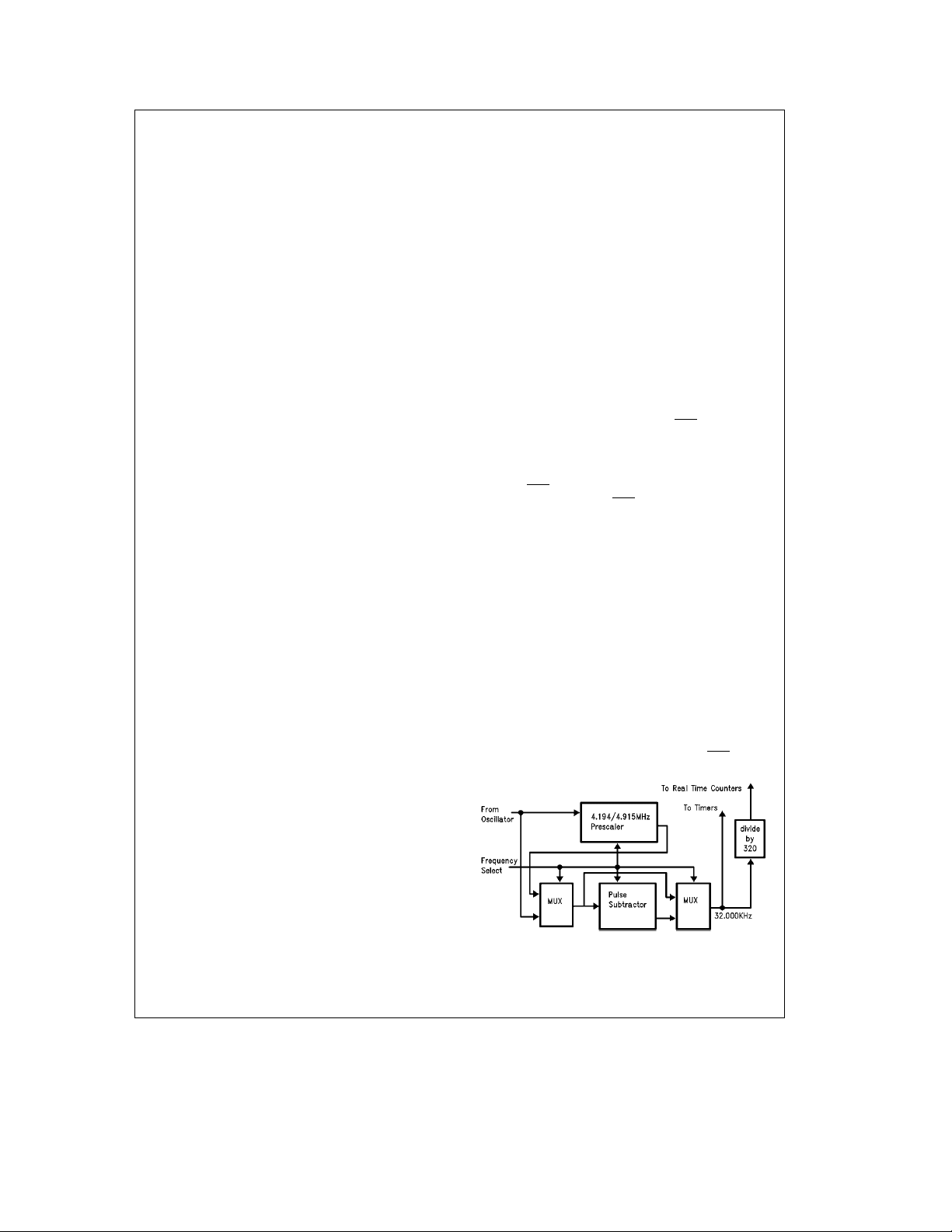
Feeding the counter chain is a programmable prescaler
which divides the crystal oscillator frequency to 32 kHz and
further to 100 Hz for the counter chain (see
Figure 3
). The
crystal frequency that can be selected are: 32 kHz, 32.768
kHz, 4.9152 MHz, and 4.194304 MHz.
Once 32 kHz is generated it feeds both timers and the
clock. The clock and timer prescalers can be independently
enabled by controlling the timer or clock Start/Stop
bits.
TL/F/9979– 7
FIGURE 3. Programmable Clock Prescaler Block
7
Functional Description (Continued)
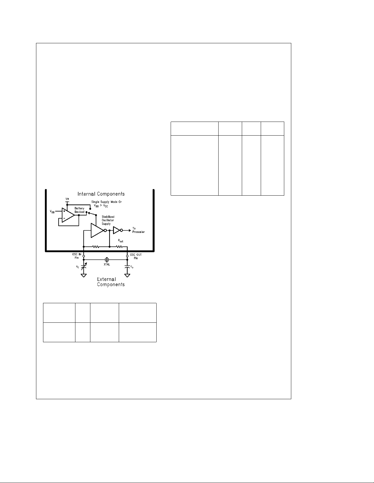
The oscillator is programmed via the Real Time Mode Register to operate at various frequencies. The crystal oscillator
is designed to offer optimum performance at each frequency. Thus, at 32.768 kHz the oscillator is configured as a low
frequency and low power oscillator. At the higher frequencies the oscillator inverter is reconfigured. In addition to the
inverter, the oscillator feedback bias resistor is included on
chip, as shown in
en from an external source if desired. Refer to test mode
application note for details. The oscillator stability is enhanced through the use of an on chip regulated power supply.
The typical range of trimmer capacitor (as shown in Oscillator Circuit Diagram
the oscillator input pin is suggested only to allow accurate
tuning of the oscillator. This range is based on a typical
printed circuit board layout and may have to be changed
depending on the parasitic capacitance of the printed circuit
board or fixture being used. In all cases, the load capaci-
tance specified by the crystal manufacturer (nominal value
11 pF for the 32.768 crystal) is what determines proper oscillation. This load capcitance is the series combination of
capacitance on each side of the crystal (with respect to
ground).
XTAL C
32/32.768 kHz 47 pF 2 pF–22 pF 150 kX to 350 kX
4.194304 MHz 68 pF 0 pF–80 pF 500X to 900X
4.9152 MHz 68 pF 29 pF–49 pF 500X to 900X
INTERRUPT LOGIC FUNCTIONAL DESCRIPTION
The TCP has the ability to coordinate processor timing activities. To enhance this, an interrupt structure has been implemented which enables several types of events to cause
interrupts. Interrupts are controlled via two Control Registers in block 1 and two Status Registers in block 0. (See
Register Description for notes on paging and also
and Table I.)
Figure 4
. The oscillator input may be driv-
Figure 4
, and in the typical application) at
FIGURE 4. Oscillator Circuit Diagram
o
C
t
(Switched
Internally)
TL/F/9979– 8
R
OUT
Figure 5
The interrupts are enabled by writing a one to the appropriate bits in Interrupt Control Register 0 and/or 1. Any of the
interrupts can be routed to either the INTR pin or the MFO
pin, depending on how the Interrupt Routing register is programmed. This, for example, enables the user to dedicate
the MFO as a non-maskable interrupt pin to the CPU for
power failure detection and enable all other interrupts to
appear on the INTR pin. The polarity for the active interrupt
can be programmed in the Output Mode Register for either
active high or low, and open drain or push pull outputs.
TABLE I. Registers that are Applicable
Register Name
Main Status Register X X 00H
Periodic Flag Register 0 0 03H
Interrupt Routing
Register
Interrupt Control
Register 0
Interrupt Control
Register 1
Output Mode
Register
The Interrupt Status Flag D0, in the Main Status Register,
indicates the state of INTR and MFO outputs. It is set when
either output becomes active and is cleared when all TCP
interrupts have been cleared and no further interrupts are
pending (i.e., both INTR and MFO are returned to their inactive state). This flag enables the TCP to be rapidly polled by
the mP to determine the source of an interrupt in a wiredÐ
OR interrupt system.
Note that the Interrupt Status Flag will only monitor the state
of the MFO output if it has been configured as an interrupt
output (see Output Mode Register description). This is true,
regardless of the state of the Interrupt Routing Register.
Thus the Interrupt Status Flag provides a true reflection of
all conditions routed to the external pins.
Status for the interrupts are provided by the Main Status
Register and the Periodic Flag Register. Bits D1 – D5 of the
Main Status Register are the main interrupt bits.
These register bits will be set when their associated timing
events occur. Enabled Alarm or Timer interrupts that occur
will set its Main Status Register bit to a one. However, an
external interrupt will only be generated if the appropriate
Alarm or Timer interrupt enable bits are set (see
Disabling the periodic bits will mask the Main Status Register periodic bit, but not the Periodic Flag Register bits. The
Power Fail Interrupt bit is set when the interrupt is enabled
and a power fail event has occurred, and is not reset until
the power is restored. If all interrupt enable bits are 0 no
interrupt will be asserted. However, status still can be read
from the Main Status Register in a polled fashion (see
ure 5
).
To clear a flag in bits D2 –D5 of the Main Status Register a 1
must be written back into the bit location that is to be
cleared. For the Periodic Flag Register reading the status
will reset all the periodic flags.
to Interrupt Control
Register Page
Select Select
0 0 04H
1 0 03H
1 0 04H
1 0 02H
Address
Figure 5
Fig-
).
8
 Loading...