NSC DM54LS502W-MLS, 5962-9080001MEA Datasheet

TL/F/10189
DM54LS502/DM74LS502 8-Bit Successive Approximation Register
April 1992
DM54LS502/DM74LS502
8-Bit Successive Approximation Register
General Description
The LS502 is an 8-bit register with the interstage logic necessary to perform serial-to-parallel conversion and provide
an active LOW Conversion Complete (CC
) signal coincident
with storage of the eighth bit. An active LOW Start (S
) input
performs synchronous initialization which forces Q7 LOW
and all other outputs HIGH. Subsequent clocks shift this Q7
LOW signal downstream which simultaneously backfills the
register such that the first serial data (D input) bit is stored in
Q7, the second bit in Q6, the third in Q5, etc. The serial
input data is also synchronized by an auxiliary flip-flop and
brought out on Q
D
.
Designed primarily for use in the successive approximation
technique for analog-to-digital conversion, the LS502 can
also be used as a serial-to-parallel converter ring counter
and as the storage and control element in recursive digital
routines.
Features
Y
Low power Schottky version of 2502
Y
Storage and control for successive approximation A to
D conversion
Y
Performs serial-to-parallel conversion
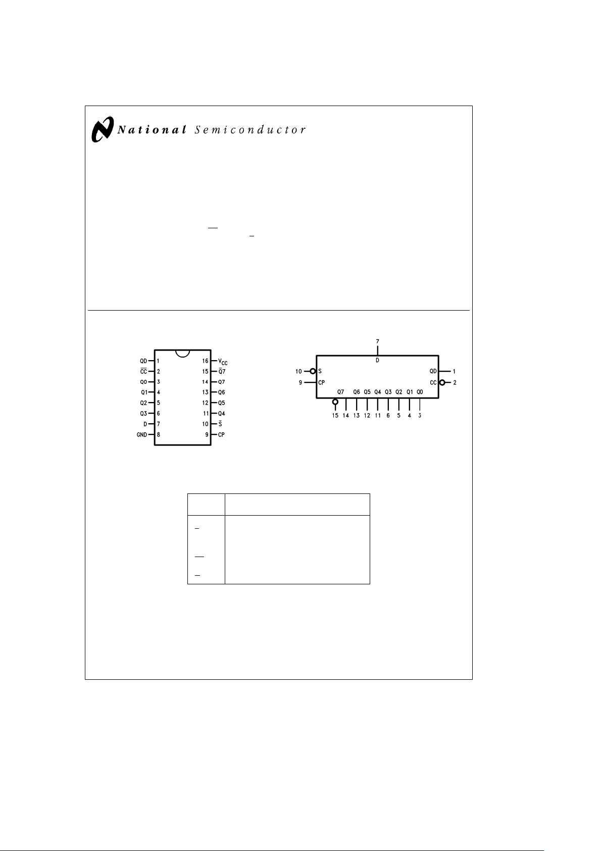
Connection Diagram
Dual-In-Line Package
TL/F/10189– 1
Order Number DM54LS502J, DM54LS502W,
DM74LS502WM or DM74LS502N
See NS Package Number J16A, M16B, N16E or W16A
Logic Symbol
TL/F/10189– 2
V
CC
e
Pin 16
GND
e
Pin 8
Pin
Description
Names
D Serial Data Input
S
Start Input (Active LOW)
CP Clock Pulse Input (Active Rising Edge)
Q
D
Synchronized Serial Data Output
CC
Conversion Complete Output (Active LOW)
Q0–Q7 Parallel Register Outputs
Q
7 Complement of Q7 Output
C
1995 National Semiconductor Corporation RRD-B30M105/Printed in U. S. A.

Absolute Maximum Ratings (Note)
If Military/Aerospace specified devices are required,
please contact the National Semiconductor Sales
Office/Distributors for availability and specifications.
Supply Voltage 7V
Input Voltage 7V
Operating Free Air Temperature Range
DM54LS
b
55§Ctoa125§C
DM74LS 0
§
Ctoa70§C
Storage Temperature Range
b
65§Ctoa150§C
Note:
The ‘‘Absolute Maximum Ratings’’ are those values
beyond which the safety of the device cannot be guaranteed. The device should not be operated at these limits. The
parametric values defined in the ‘‘Electrical Characteristics’’
table are not guaranteed at the absolute maximum ratings.
The ‘‘Recommended Operating Conditions’’ table will define
the conditions for actual device operation.
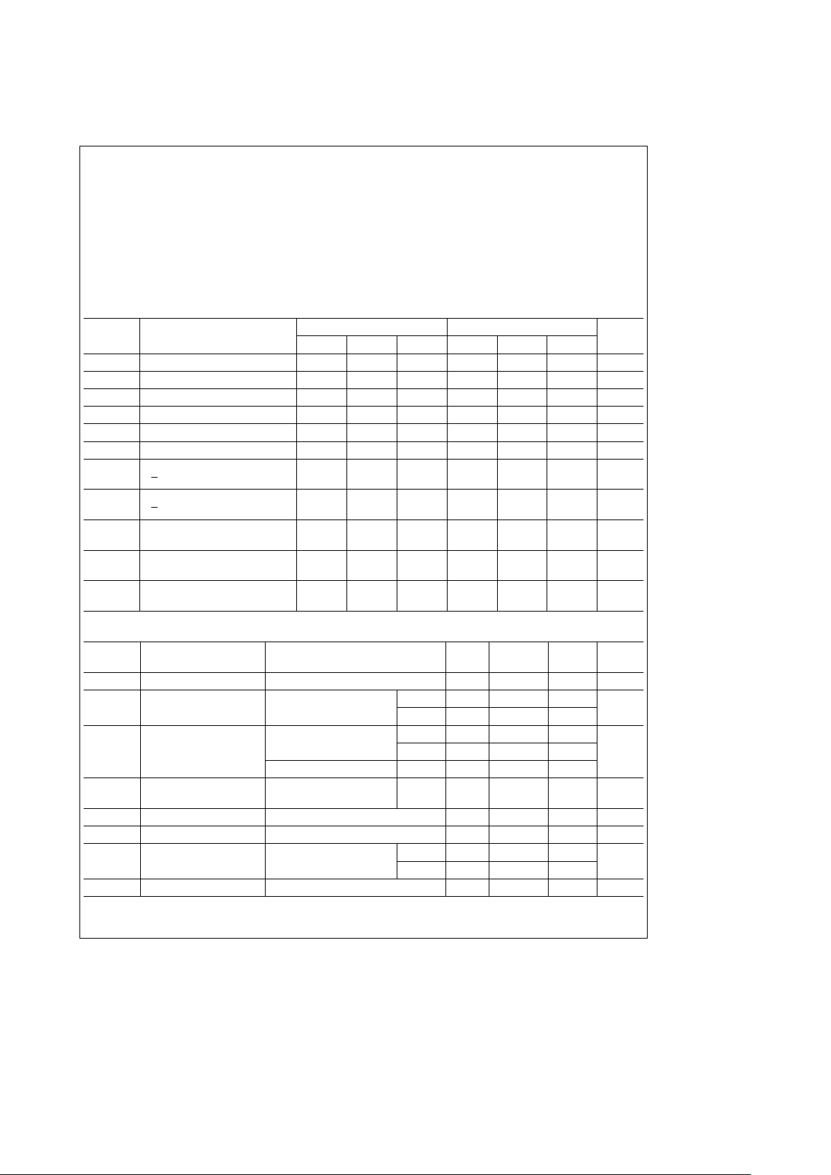
Recommended Operating Conditions
Symbol Parameter
DM54LS502 DM74LS502
Units
Min Nom Max Min Nom Max
V
CC
Supply Voltage 4.5 5 5.5 4.75 5 5.25 V
V
IH
High Level Input Voltage 2 2 V
V
IL
Low Level Input Voltage 0.7 0.8 V
I
OH
High Level Output Current
b
0.4
b
0.4 mA
I
OL
Low Level Output Current 4 8 mA
T
A
Free Air Operating Temperature
b
55 125 0 70
§
C
ts(H) Setup Time HIGH or LOW 5 16
ns
t
s
(L) S to CP 5 16
th(H) Hold Time HIGH or LOW 5 0
ns
th(L) S to CP 5 0
ts(H) Setup Time HIGH or LOW 5 8
ns
t
s
(L) DtoCP 5 8
th(H) Hold Time HIGH or LOW 5 10
ns
t
h
(L) D to CP 5 10
tw(H) CP Pulse Width HIGH or LOW 20 46
ns
t
w
(L) 20 46
Electrical Characteristics over recommended operating free air temperature range (unless otherwise noted)
Symbol Parameter Conditions Min
Typ
Max Units
(Note 1)
V
I
Input Clamp Voltage V
CC
e
Min, I
I
eb
18 mA
b
1.5 V
V
OH
High Level Output V
CC
e
Min, I
OH
e
Max, DM54 2.5
V
Voltage V
IL
e
Max
DM74 2.7
V
OL
Low Level Output VCCMin, I
OL
e
Max, DM54 0.4
Voltage V
IH
e
Min
DM74 0.5 V
I
OL
e
4 mA, V
CC
e
Min DM74 0.4
I
I
Input Current@Max V
CC
e
Max, V
I
e
7V DM74
0.1 mA
Input Voltage V
I
e
10V DM54
I
IH
High Level Input Current V
CC
e
Max, V
I
e
2.7V 20 mA
I
IL
Low Level Input Current V
CC
e
Max, V
I
e
0.4V
b
0.8 mA
I
OS
Short Circuit V
CC
e
Max DM54
b
20
b
100
mA
Output Current (Note 2)
DM74
b
20
b
100
I
CC
Supply Current V
CC
e
Max 65 mA
Note 1: All typicals are at V
CC
e
5V, T
A
e
25§C.
Note 2: Note more than one output should be shorted at a time, and the duration should not exceed one second.
2
 Loading...