NSC DM54LS279J-883 Datasheet

TL/F/6420
54LS279/DM54LS279/DM74LS279 Quad S-R Latches
May 1989
54LS279/DM54LS279/DM74LS279
Quad S
-R Latches
General Description
The ’LS279 consists of four individual and independent SetReset Latches with active low inputs. Two of the four latches have an additonal S
input ANDed with the primary S
input. A low on any S input while the R input is high will be
stored in the latch and appear on the corresponding Q output as a high. A low on the R
input while the S input is high
will clear the Q output to a low. Simultaneous transistion of
the R
and S inputs from low to high will cause the Q output
to be indeterminate. Both inputs are voltage level triggered
and are not affected by transition time of the input data.
Features
Y
Alternate military/aerospace device (54LS279) is available. Contact a National Semiconductor Sales Office/
Distributor for specifications.
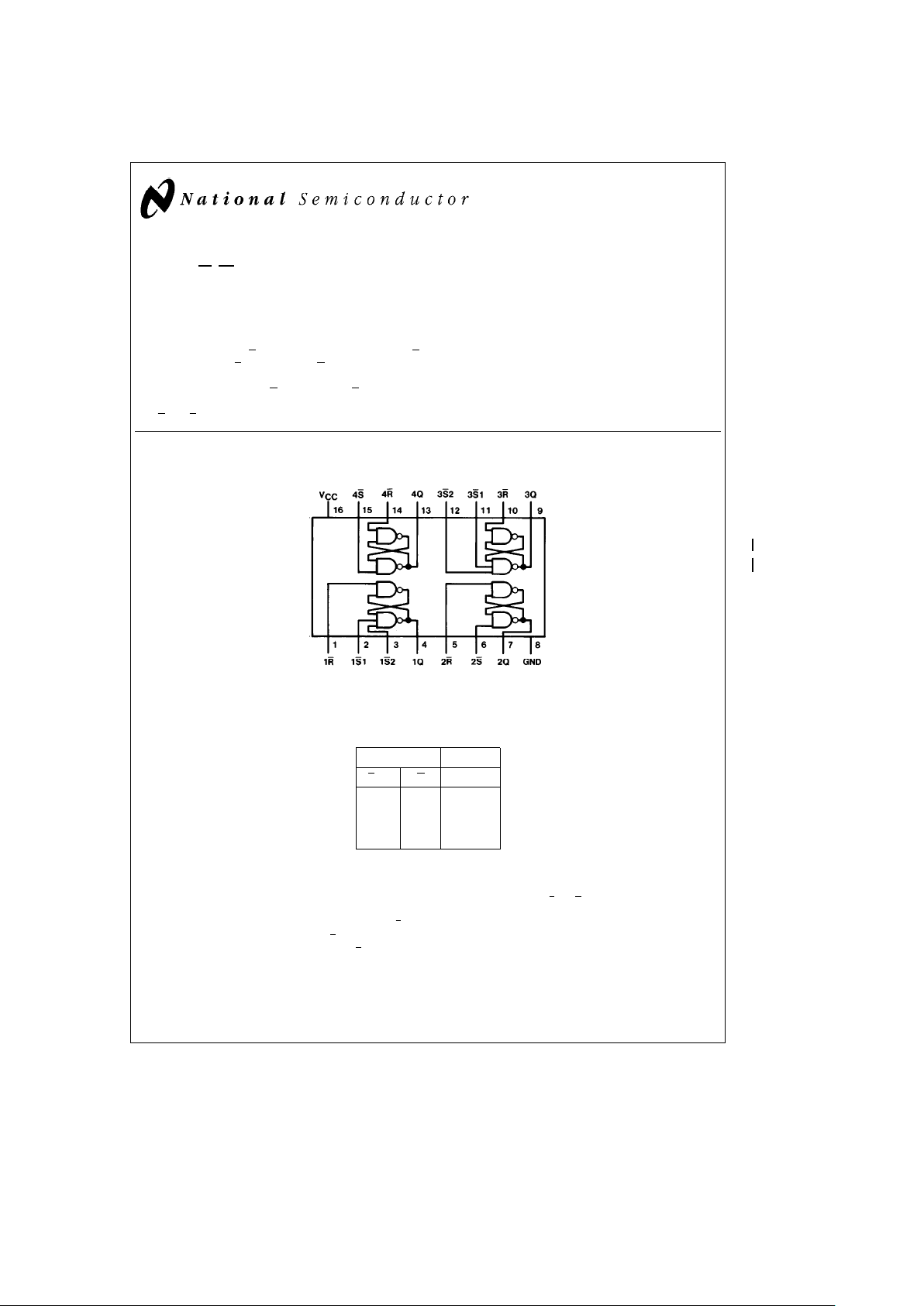
Connection Diagram
Dual-In-Line Package
TL/F/6420– 1
Order Number 54LS279DMQB, 54LS279FMQB, 54LS279LMQB,
DM54LS279J, DM74LS279M or DM74LS279N
See NS Package Number E20A, J16A, M16A, N16E or W16A
Function Table
Inputs Output
S(1) R Q
LL H*
LH H
HL L
HH Q
0
H
e
High Level
L
e
Low Level
Q
0
e
The Level of Q before the indicated input conditions were established.
*This output level is pseudo stable; that is, it may not persist when the S
and R
inputs return to their inactive (high) level.
Note 1: For latches with double S
inputs:
H
e
both S inputs high
L
e
one or both S inputs low
C
1995 National Semiconductor Corporation RRD-B30M105/Printed in U. S. A.

Absolute Maximum Ratings (Note)
If Military/Aerospace specified devices are required,
please contact the National Semiconductor Sales
Office/Distributors for availability and specifications.
Supply Voltage 7V
Input Voltage 7V
Operating Free Air Temperature Range
DM54LS and 54LS
b
55§Ctoa125§C
DM74LS 0
§
Ctoa70§C
Storage Temperature Range
b
65§Ctoa150§C
Note:
The ‘‘Absolute Maximum Ratings’’ are those values
beyond which the safety of the device cannot be guaranteed. The device should not be operated at these limits. The
parametric values defined in the ‘‘Electrical Characteristics’’
table are not guaranteed at the absolute maximum ratings.
The ‘‘Recommended Operating Conditions’’ table will define
the conditions for actual device operation.
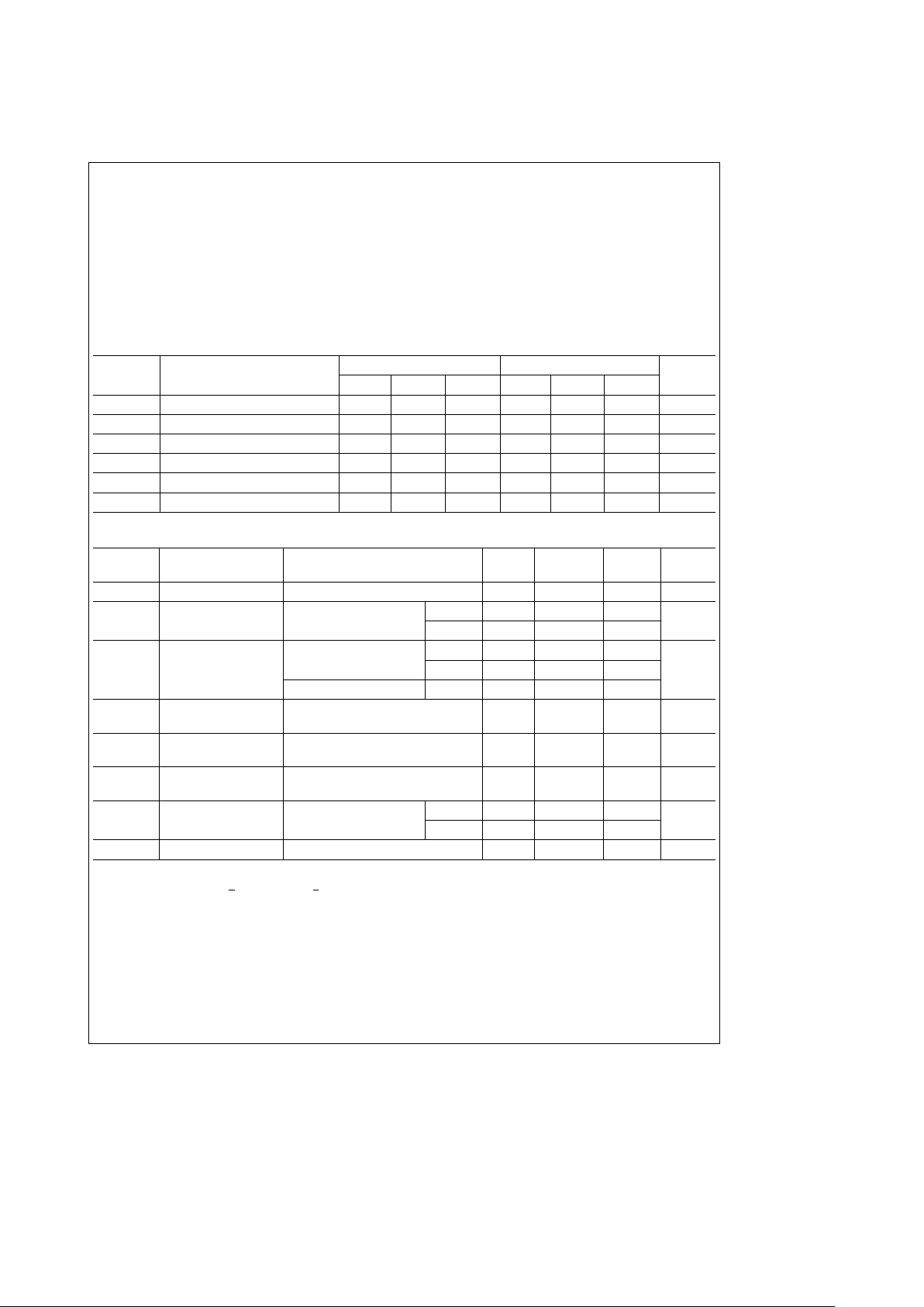
Recommended Operating Conditions
Symbol Parameter
DM54LS279 DM74LS279
Units
Min Nom Max Min Nom Max
V
CC
Supply Voltage 4.5 5 5.5 4.75 5 5.25 V
V
IH
High Level Input Voltage 2 2 V
V
IL
Low Level Input Voltage 0.7 0.8 V
I
OH
High Level Output Current
b
0.4
b
0.4 mA
I
OL
Low Level Output Current 4 8 mA
T
A
Free Air Operating Temperature
b
55 125 0 70
§
C
Electrical Characteristics over recommended operating free air temperature range (unless otherwise noted)
Symbol Parameter Conditions Min
Typ
Max Units
(Note 1)
V
I
Input Clamp Voltage V
CC
e
Min, I
I
eb
18 mA
b
1.5 V
V
OH
High Level Output V
CC
e
Min, I
OH
e
Max DM54 2.5 3.5
V
Voltage
V
IL
e
Max, V
IH
e
Min DM74 2.7 3.5
V
OL
Low Level Output V
CC
e
Min, I
OL
e
Max DM54 0.25 0.4
Voltage V
IL
e
Max, V
IH
e
Min
DM74 0.35 0.5 V
I
OL
e
4 mA, V
CC
e
Min DM74 0.25 0.4
I
I
Input Current@Max V
CC
e
Max, V
I
e
7V
0.1 mA
Input Voltage
I
IH
High Level Input V
CC
e
Max, V
I
e
2.7V
20 mA
Current
I
IL
Low Level Input V
CC
e
Max, V
I
e
0.4V
b
0.4 mA
Current
I
OS
Short Circuit V
CC
e
Max DM54
b
20
b
100
mA
Output Current (Note 2)
DM74
b
20
b
100
I
CC
Supply Current V
CC
e
Max (Note 3) 3.8 7 mA
Note 1: All typicals are at V
CC
e
5V, T
A
e
25§C.
Note 2: Not more than one output should be shorted at a time, and the duration should not exceed one second.
Note 3: I
CC
is measured with all R inputs grounded, all S inputs at 4.5V and all outputs open.
2
 Loading...