NSC DM54LS259J-883 Datasheet

TL/F/6418
DM54LS259/DM74LS259 8-Bit Addressable Latches
May 1992
DM54LS259/DM74LS259 8-Bit Addressable Latches
General Description
These 8-bit addressable latches are designed for general
purpose storage applications in digital systems. Specific
uses include working registers, serial-holding registers, and
active-high decoders or demultiplexers. They are multifunctional devices capable of storing single-line data in eight
addressable latches, and being a 1-of-8 decoder or demultiplexer with active-high outputs.
Four distinct modes of operation are selectable by controlling the clear and enable inputs as enumerated in the function table. In the addressable-latch mode, data at the datain terminal is written into the addressed latch. The addressed latch will follow the data input with all unaddressed
latches remaining in their previous states. In the memory
mode, all latches remain in their previous states and are
unaffected by the data or address inputs. To eliminate the
possibility of entering erroneous data in the latches, the enable should be held high (inactive) while the address lines
are changing. In the 1-of-8 decoding or demultiplexing
mode, the addressed output will follow the level of the D
input with all other outputs low. In the clear mode, all outputs are low and unaffected by the address and data inputs.
Features
Y
8-Bit parallel-out storage register performs serial-to-parallel conversion with storage
Y
Asynchronous parallel clear
Y
Active high decoder
Y
Enable/disable input simplifies expansion
Y
Direct replacement for Fairchild 9334
Y
Expandable for N-bit applications
Y
Four distinct functional modes
Y
Typical propagation delay times:
Enable-to-output 18 ns
Data-to-output 16 ns
Address-to-output 21 ns
Clear-to-output 17 ns
Y
Fan-out
I
OL
(sink current)
54LS259 4 mA
74LS259 8 mA
I
OH
(source current)b0.4 mA
Y
Typical ICC22 mA
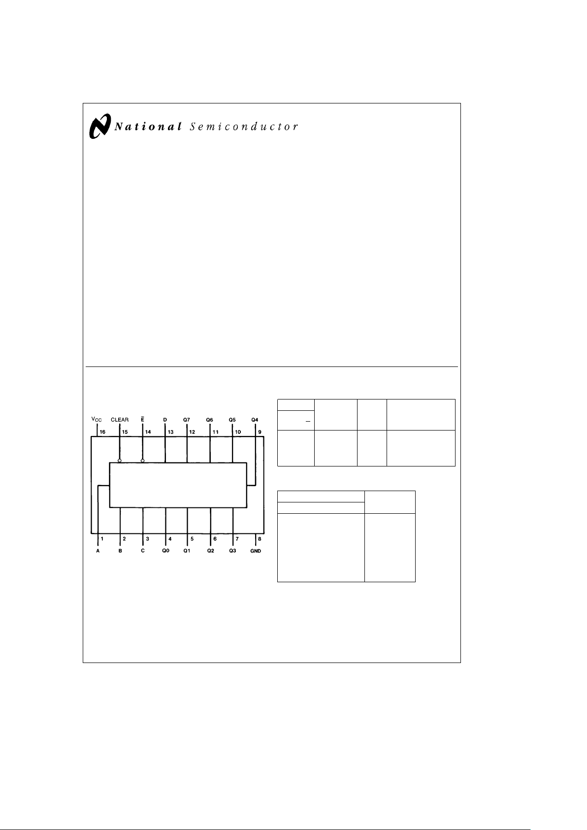
Connection Diagram
Dual-In-Line Package
TL/F/6418– 1
Order Number DM54LS259E, DM54LS259J,
DM54LS259W, DM74LS259M,
DM74LS259WM or DM74LS259N
See NS Package Number E20A, J16A,
M16A, M16B, N16E or W16A
Function Table
Inputs Output of Each
Addressed Other Function
Clear E
Latch Output
HL D Qi0Addressable Latch
HH Q
i0
Qi0Memory
L L D L 8-Line Demultiplexer
L H L L Clear
Latch Selection Table
Select Inputs
Latch
CBA
Addressed
LLL 0
LLH 1
LHL 2
LHH 3
HLL 4
HLH 5
HHL 6
HHH 7
H
e
High Level, LeLow Level
D
e
the Level of the Data Input
Q
i0
e
the Level of Qi(ie0, 1, . . . 7, as Appropriate) before the Indicated
Steady-State Input Conditions Were Established.
C
1995 National Semiconductor Corporation RRD-B30M105/Printed in U. S. A.

Absolute Maximum Ratings (Note)
If Military/Aerospace specified devices are required,
please contact the National Semiconductor Sales
Office/Distributors for availability and specifications.
Supply Voltage 7V
Input Voltage 7V
Operating Free Air Temperature Range
DM54
b
55§Ctoa125§C
DM74LS 0
§
Ctoa70§C
Storage Temperature Range
b
65§Ctoa150§C
Note:
The ‘‘Absolute Maximum Ratings’’ are those values
beyond which the safety of the device cannot be guaranteed. The device should not be operated at these limits. The
parametric values defined in the ‘‘Electrical Characteristics’’
table are not guaranteed at the absolute maximum ratings.
The ‘‘Recommended Operating Conditions’’ table will define
the conditions for actual device operation.
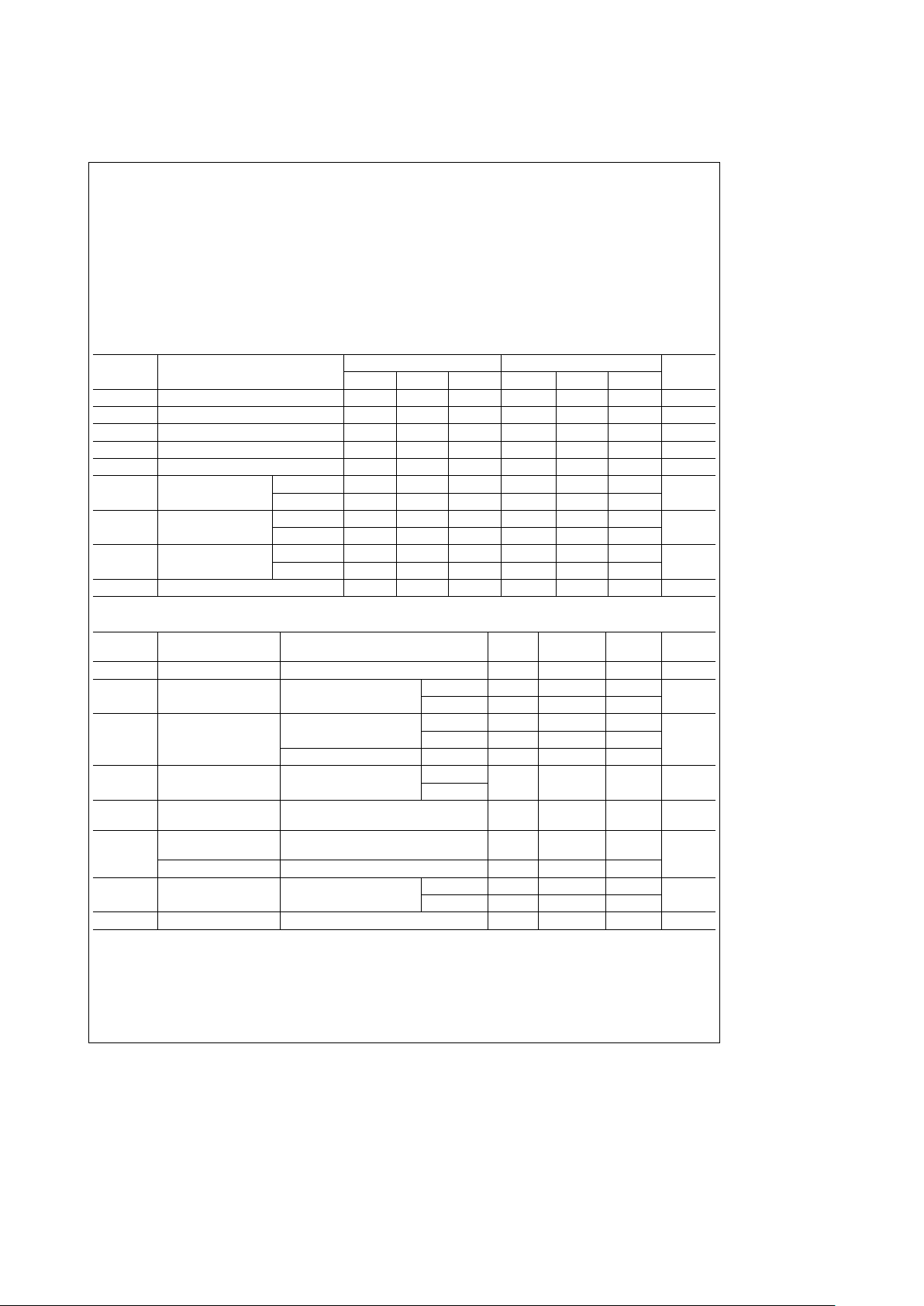
Recommended Operating Conditions
Symbol Parameter
DM54LS259 DM74LS259
Units
Min Nom Max Min Nom Max
V
CC
Supply Voltage 4.5 5 5.5 4.75 5 5.25 V
V
IH
High Level Input Voltage 2 2 V
V
IL
Low Level Input Voltage 0.7 0.8 V
I
OH
High Level Output Current
b
0.4
b
0.4 mA
I
OL
Low Level Output Current 4 8 mA
t
W
Pulse Width Enable 17 15
ns
(Note 7)
Clear 17 15
t
SU
Setup Time Data 20
u
15
u
ns
(Notes 1, 2,3&7)
Select 15
v
15
v
t
H
Hold Time Data 5
u
2.5
u
ns
(Notes 1,2&7)
Select 0
u
2.5
u
T
A
Free Air Operating Temperature
b
55 125 0 70
§
C
Electrical Characteristics over recommended operating free air temperature range (unless otherwise noted)
Symbol Parameter Conditions Min
Typ
Max Units
(Note 4)
V
I
Input Clamp Voltage V
CC
e
Min, I
I
eb
18 mA
b
1.5 V
V
OH
High Level Output V
CC
e
Min, I
OH
e
Max DM54 2.5
V
Voltage V
IL
e
Max, V
IH
e
Min
DM74 2.7 3.4
V
OL
Low Level Output V
CC
e
Min, I
OL
e
Max DM54 0.4
Voltage V
IL
e
Max, V
IH
e
Min
DM74 0.35 0.5 V
I
OL
e
4 mA, V
CC
e
Min DM74 0.25 0.4
I
I
Input Current@Max V
CC
e
Max, V
I
e
7V DM74
0.1 mA
Input Voltage V
I
e
10V
DM54
I
IH
High Level Input V
CC
e
Max, V
I
e
2.7V
20 mA
Current
I
IL
Low Level Input V
CC
e
Max, V
I
e
0.4V
b
0.4
Current mA
Enable V
CC
e
Max, V
I
e
0.4V
b
0.8
I
OS
Short Circuit V
CC
e
Max DM54
b
20
b
100
mA
Output Current (Note 5)
DM74
b
20
b
100
I
CC
Supply Current V
CC
e
Max (Note 6) 22 36 mA
Note 1: The symbols (v,u) indicate the edge of the clock pulse used for reference:ufor rising edge,vfor falling edge.
Note 2: Setup and hold times are with reference to the enable input.
Note 3: The select-to-enable setup time is the time before the High-to-Low enable transition that the select must be stable so that the correct latch is selected and
the others not affected.
Note 4: All typicals are at V
CC
e
5V, T
A
e
25§C.
Note 5: Not more than one output should be shorted at a time, and the duration should not exceed one second.
Note 6: I
CC
is measured with all inputs at 4.5V, and all outputs open.
Note 7: T
A
e
25§C and V
CC
e
5V.
2
 Loading...