Features
■
450MHz small signal bandwidth
■
2000 V/µs slew rate
■
5mA / channel supply current
■
-71/-82dBc HD2/HD3 (5MHz)
■
0.03%, 0.03° differential gain, phase
■
70mA output current
■
12ns settling to 0.1%
Applications
■
High performance RGB video
■
Video switchers & routers
■
Video line driver
■
Active filters
■
IF amplifier
■
Twisted pair driver/receiver
Pinout
DIP & SOIC
General Description
The CLC5654 is a quad, current feedback operational amplifier
that is perfect for many cost-sensitive applications that require
high performance. This device also offers excellent economy
in board space and power, consuming only 5mA per amplifier
while providing 70mA of output current capability. Applications
requiring significant density of high speed devices such as video
routers, matrix switches and high-order active filters will benefit
from the configuration of the CLC5654 and the low channel-tochannel crosstalk of 70dB at 5MHz.
The CLC5654 provides excellent performance for video
applications. Differential gain and phase of 0.03% and 0.03°
makes this device well suited for many professional composite
video systems, but consumer applications will also be able to tak e
advantage of these features due to the device’s low cost. The
CLC5654 offers superior dynamic performance with a small
signal bandwidth of 450MHz and slew rate of 2000V/µs. These
attributes are well suited for many component video applications
such as driving RGB signals down significant lengths of cable.
These and many other application can also take advantage of the
0.1dB flatness to 40MHz.
Combining wide bandwidth with low cost makes the the CLC5654
an attractive option for active filters. SAW filters are often used
in IF filters in the 10’s of MHz range, but higher order filters
designed around a quad operational amplifier may offer an
economical alternative to the typical SAW approach and offer
greater freedom in the selection of filter parameters. National
Semiconductor’s Comlinear Products Group has published
a wide array of liturature on active filters and a list of these
publications can be found on the last page of this datasheet.
CLC5654
Very High-Speed, Low-Cost, Quad Operational Amplifier
N
June 1999
CLC5654
Very High-Speed, Low-Cost, Quad Operational Amplifier
© 1999 National Semiconductor Corporation http://www.national.com
Printed in the U.S.A.
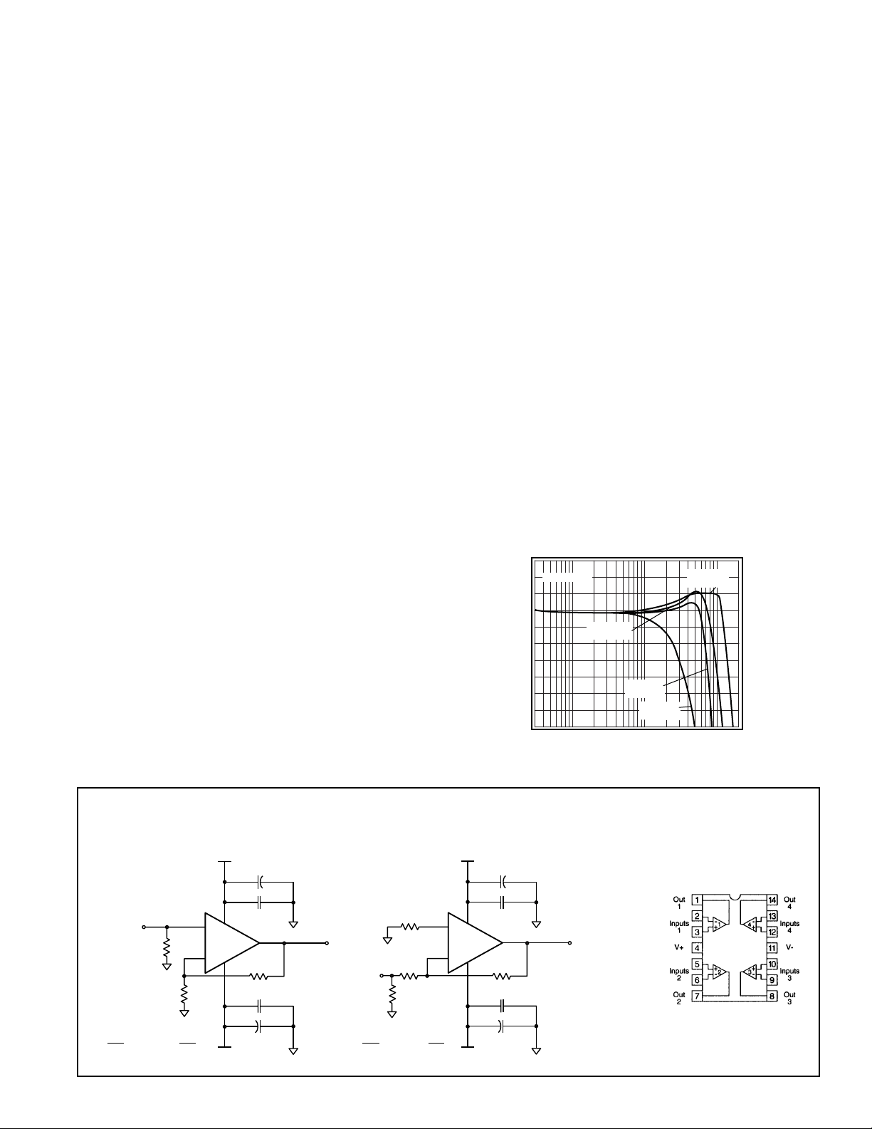
Typical Configurations
Non-Inverting Gain Inverting Gain
Non-Inverting Frequency Response
Vo = 0.25V
pp
Av = +1
Rf = 2.21kΩ
Av = +5
Rf = 402Ω
Av = +10
Normalized Magnitude (0.5dB/div)
1M
Rf = 200Ω
10M
Frequency (Hz)
Av = +2
Rf = 866Ω
100M
V
CC
6.8µF
+
V
in
R
t
R
g
V
o
A1
==+
V
in
R
v
f
R
g
+
1/4
CLC5654
-
V
EE
0.1µF
R
f
0.1µF
6.8µF
V
o
+
V
in
R
t
V
o
A
==−
V
in
R
b
R
g
v
V
CC
6.8µF
+
0.1µF
+
1/4
CLC5654
R
f
0.1µF
R
f
R
g
V
EE
+
6.8µF
V
o
Note: Rb provides DC bias
for the non-inverting input.
Select R
to yield desired
t
Rin = Rt || Rg.

http://www.national.com 2
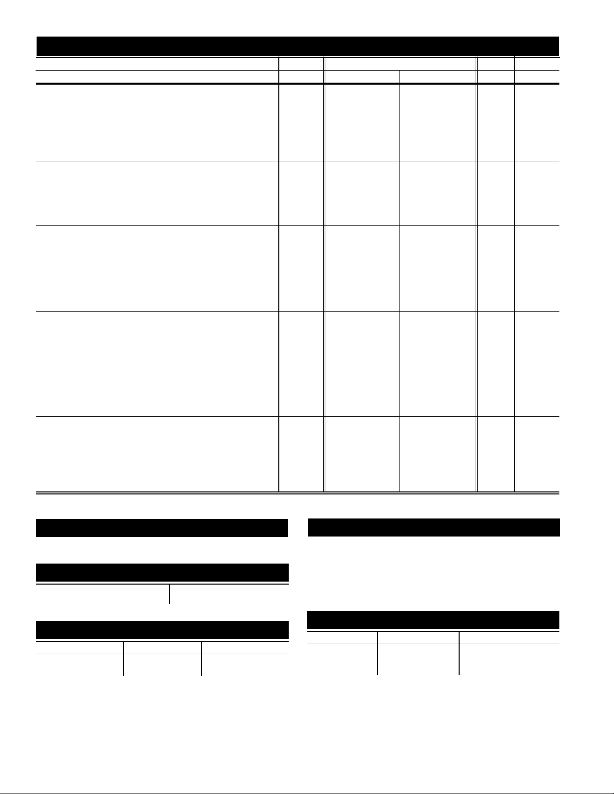
PARAMETERS CONDITIONS TYP MIN/MAX RATINGS UNITS NOTES
Ambient Temperature CLC5654I +25°C +25°C -40 to 85°C
FREQUENCY DOMAIN RESPONSE
-3dB bandwidth A
v
= 1 450 – – MHz
V
o
< 0.5V
pp
350 – – MHz
V
o
< 5V
pp
100 – – MHz
0.1dB bandwidth 40 – – MHz
differential gain NTSC, R
L
= 150Ω 0.03 – – dB
differential phase NTSC, R
L
= 150Ω 0.03 – – dB
TIME DOMAIN RESPONSE
rise and fall time 0.5V step 1.2 – – ns
5V step 2.7 – – ns
settling time to 0.1% 2V step 12 – – ns
overshoot 0.5V step 7 – – %
slew rate 2000 – – V/µs
DISTORTION AND NOISE RESPONSE
2ndharmonic distortion 2Vpp, 5MHz -71 – – dBc
3
rd
harmonic distortion 2Vpp, 5MHz -82 – – dBc
equivalent input noise
voltage (e
ni
) >1MHz 3.3 – – nV/√Hz
non-inverting current (i
bn
) >1MHz 2.5 – – pA/√Hz
inverting current (i
bi
) >1MHz 12 – – pA/√Hz
crosstalk (input inferred) 10MHz 76 – – dBc
STATIC DC PERFORMANCE
input offset voltage 2.5 6 11 mV A
average drift 18 – 55 µV/˚C
input bias current (non-inverting) 6 15 28 µAA
average drift 40 – 160 nA/˚C
input bias current (inverting) 5 12 20 µAA
average drift 25 – 120 nA/˚C
power supply rejection ratio DC 55 47 45 dB
common-mode rejection ratio DC 50 45 43 dB
supply current (per channel) R
L
= ∞ 5 6.7 7 mA A
MISCELLANEOUS PERFORMANCE
input resistance (non-inverting) 1 0.5 0.25 MΩ
input capacitance (non-inverting) 1 2 2 pF
common-mode input range ±2.2 ±2.0 ±1.4 V
output voltage range R
L
= 150Ω ±2.6 ±2.5 ±2.3 V
output current 70 50 40 mA
output resistance, closed loop DC 0.2 0.3 0.6 mΩ
Min/max ratings are based on product characterization and simulation. Individual parameters are tested as noted. Outgoing quality levels are
determined from tested parameters.
CLC5654 Electrical Characteristics
(Av= +2, Rf= 866Ω,RL= 100Ω,Vs= ±5V, unless specified)
Absolute Maximum Ratings
supply voltage (VCC- VEE)
+
14V
output current 95mA
common-mode input voltage
VEEto
V
CC
maximum junction temperature +150°C
storage temperature range -65°C to +150°C
lead temperature (soldering 10 sec) +300°C
Notes
A) J-level:spec is 100% tested at +25°C.
Reliability Information
Transistor Count 152
MTBF (based on limited test data) 12.5Mhr
Ordering Information
Model Temperature Range Description
CLC5654IN -40°C to +85°C 14-pin PDIP
CLC5654IM -40°C to +85°C 14-pin SOIC
CLC5654IMX -40°C to +85°C 14-pin tape and reel
Pac kage Thermal Resistance
Package
θθ
JC
θθ
JA
Plastic (IN) 60°C/W 110°C/W
Surface Mount (IM) 55°C/W 125°C/W
 Loading...