NSC CLC427AJP Datasheet

Features
■
Single +5V supply
■
Input includes V
EE
■
94MHz unity-gain bandwidth
■
-74/-94dBc HD2/HD3
■
60mA output current
■
7.5ns rise/fall time (1Vpp)
■
46ns settling time to 0.1%
Applications
■
Video ADC driver
■
Desktop multimedia
■
Single supply cable driver
■
Instrumentation
■
Video cards
■
Wireless IF amplifiers
■
Telecommunications
General Description
The Comlinear CLC427 is a dual wideband voltage-feedback
operational amplifier that is uniquely designed to provide high
performance from a single power supply. This CLC427 provides
near rail-to-rail operation and the common-mode input range
includes the negative rail. Each of the CLC427’s amplifiers offers
plenty of headroom for single-supply applications as evidenced
by its 4.3Vppoutput voltage from a single 5V supply.
Fabricated with a high-speed complementary bipolar process,
the CLC427 delivers a wide 94MHz unity-gain bandwidth, 7.5ns
rise/fall time and 150V/µs slew rate. For single supply applications
such as video distribution or desktop multimedia, the CLC427
offers low 0.35%, 0.55° differential gain and phase errors.
Each of the CLC427’s amplifiers provides high signal fidelity
with -74/-94dBc 2nd/3rd harmonics (1Vpp, 1MHz, RL=150Ω).
Combining this high fidelity performance with CLC427’s quick
46ns settling time to 0.1% makes it an excellent choice for ADC
buffering.
With its traditional voltage-feedback architecture and high-speed
performance, the CLC427 is the perfect choice for composite
signal conditioning circuit functions such as active filters,
integrators, differentiators, simple gain blocks and buffering.
V
in
50Ω
250Ω
+
-
250Ω
0.1µF
6.8µF
150Ω
NOTE: Vin = 0.15V to 2.3V
1/2
CLC427
V
o
+5V
+
Typical Application
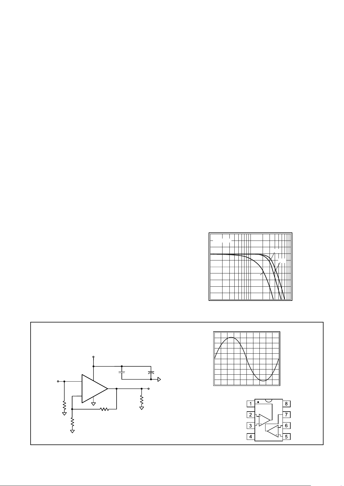
Single +5V Supply operation
Comlinear CLC427
Dual Voltage Feedback Amplifier
for Single Supply Operation
Frequency Response vs. V
out
Magnitude (1dB/div)
Frequency (MHz)
1
10
100
1V
pp
2V
pp
4V
pp
Av = +2V/V
V
o1
V
inv1
V
non-inv1
V
EE
V
o2
V
inv2
V
non-inv2
V
CC
Pinout
DIP & SOIC
Single Supply Response
Output Voltage (V)
Time (100ns/div)
VEE 0
1
2
3
4
V
CC
5
August 1996
Comlinear CLC427
Dual Voltage Feedback Amplifier for Single Supply Operation
N
© 1996 National Semiconductor Corporation http://www.national.com
Printed in the U.S.A.

http://www.national.com 2
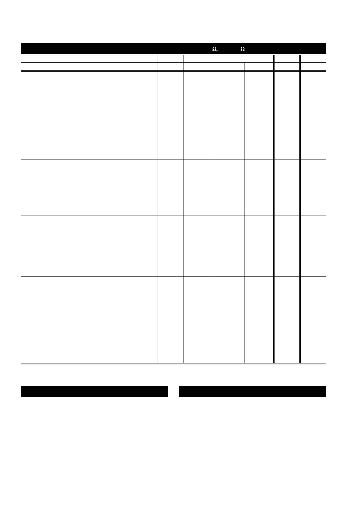
PARAMETERS CONDITIONS TYP MIN/MAX RATINGS UNITS NOTES
CLC427AJ 25° 25° 0° to +70° -40° to +85°
FREQUENCY DOMAIN RESPONSE
-3dB bandwidth V
o
< 1.0V
pp
48 32 28 27 MHz B
-3dB bandwidth V
o
< 3.0V
pp
26 16 14 11 MHz
-3dB bandwidth A
V
= +1V/V Vo< 1.0V
pp
94 MHz
rolloff <10MHz 0.1 0.5 0.7 0.8 dB B
peaking DC to 200MHz 0 0.5 0.7 0.8 dB B
linear phase deviation <15MHz 0.3 0.6 0.8 0.9 deg
differential gain NTSC, R
L
=150Ω 0.35 0.7 – – % 2
differential phase NTSC, R
L
=150Ω 0.55 2 – – deg 2
TIME DOMAIN RESPONSE
rise and fall time 1V step 7.5 13 14 16 ns
settling time to 0.1% 1V step 46 70 – – ns
overshoot 1V step 5 13 – – %
slew rate A
V
= +2 2V step 150 90 83 65 V/µs
DISTORTION AND NOISE RESPONSE
2
nd
harmonic distortion 1Vpp, 1MHz 74 – – – -dBc
1V
pp
, 5MHz 62 55 52 52 -dBc B
3
rd
harmonic distortion 1Vpp, 1MHz 94 – – – -dBc
1V
pp
, 5MHz 75 65 63 62 -dBc B
equivalent input noise
voltage >1MHz 10 12.5 13.6 14 nV/√Hz
current >1MHz 4 5 5.5 5.7 pA/√Hz
crosstalk, input referred 10MHz 65 59 59 59 -dB
STATIC DC PERFORMANCE
input offset voltage 2 7 8 10 mV A
average drift 4 – 22 35 µV/˚C
input bias current 17 30 36 45 µAA
average drift 80 – 145 175 nA/˚C
input offset current 0.2 5 6 7.5 µA
average drift 10 – 22 27 nA/˚C
power supply rejection ratio DC 82 65 64 60 dB B
common-mode rejection ratio DC 82 55 53 50 dB
supply current (per amplifier) no load 7 8.5 8.5 8.5 mA A
MISCELLANEOUS PERFORMANCE
input capacitance 1 2 2 2 pF
input resistance 700 500 450 360 kΩ
output impedance @DC 0.07 0.15 0.24 0.7 Ω
input voltage range, high 3.7 3.45 3.25 3.15 V
input voltage range, low 0 0 0 0 V
output voltage range, high R
L
= 150Ω 4.5 4.35 4.3 4.2 V
output voltage range, low R
L
= 150Ω 0.35 0.5 0.5 0.55 V
output voltage range, high no load 4.8 4.6 4.55 4.45 V
output voltage range, low no load 0.45 0.65 0.7 0.75 V
output current source 60 50 40 34 mA
output current sink 36 20 16 10 mA
supply voltage, maximum 7 7 7 V 1
supply voltage, minimum 4 4 4 V 1
transistor count = 124
Min/max ratings are based on product characterization and simulation. Individual parameters are tested as noted. Outgoing quality levels are
determined from tested parameters.
Electrical Characteristics
(Vs= +5V1, Vcm= +2.5V, Av= +2, Rf= 250
W,
RL= 150Wto GND; unless specified)
Absolute Maximum Ratings
supply voltage (Vs)
+7
V
I
out
is short circuit protected to ground
common-mode input voltage
VEEto V
CC
maximum junction temperature +175˚C
storage temperature range -65˚C to +150˚C
lead temperature (soldering 10 sec) +260˚C
differential input voltage ±2V
ESD tolerance (Note 3) 2000V
Notes
A)J-level: spec is 100% tested at 25°C, sample tested at 85°C.
B)J-level: spec is sample tested at 25°C.
1) V
s
= VCC– VEE.
2) Tested with R
L
tied to +2.5V.
3) Human body model, 1.5kΩ in series with 100pF.

3 http://www.national.com
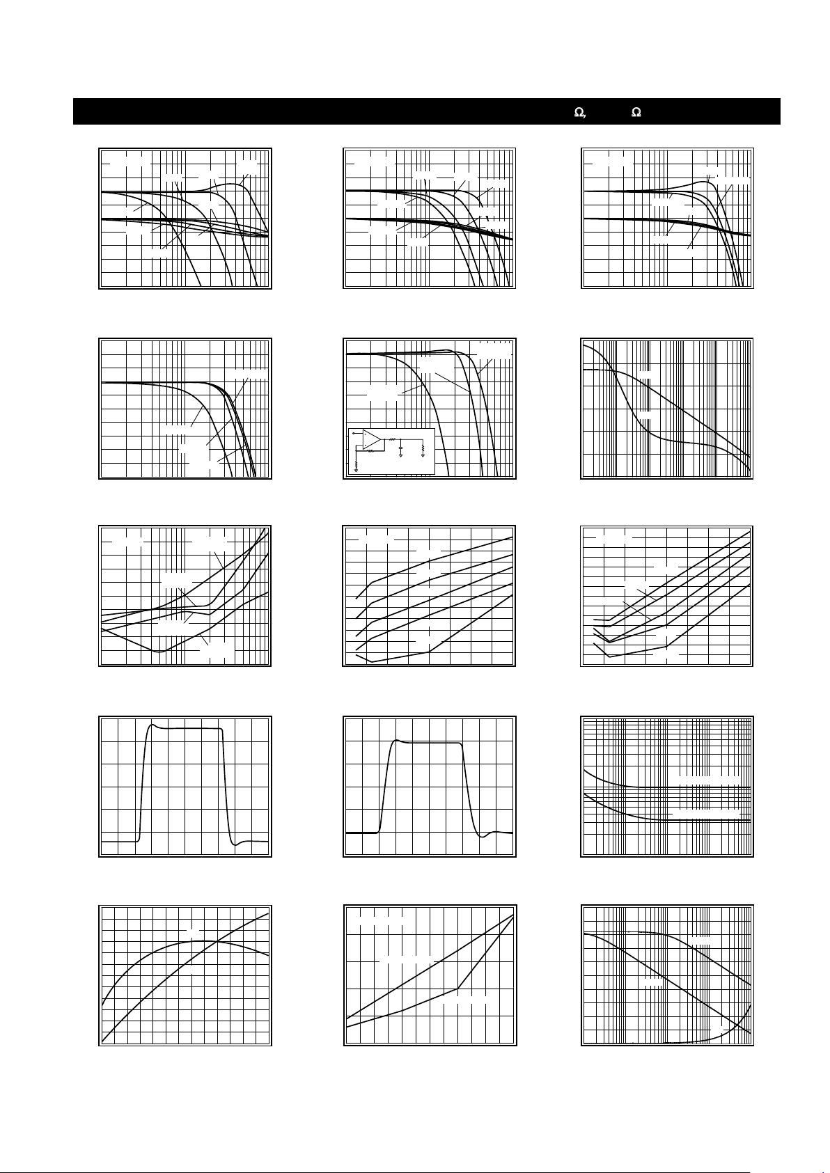
Typical Performance Characteristics
(Vs= +5V1, Vcm= +2.5V , Av= +2, Rf=250
W,
RL= 150Wto GND; unless specified)
Non-Inverting Frequency Response
Magnitude (1dB/div)
Frequency (MHz)
1
10
100
Av = 1
Rf = 0
Phase (deg)
-225
-180
-135
-90
-45
0
Av = 2
Av = 4
Av = 10
Av = 10
Av = 4
Av = 2
Av = 1
Vo = 0.25V
pp
Inverting Frequency Response
Magnitude (1dB/div)
Frequency (MHz)
1
10
100
Av = -1
Phase (deg)
-45
0
45
90
135
180
Av = -2
Av = -5
Av = -10
Av = -10
Av = -5
Av = -2
Av = -1
Vo = 0.25V
pp
Frequency Response vs. R
L
Magnitude (1dB/div)
Frequency (MHz)
0
10
100
RL = 1kΩ
Phase (deg)
-225
-180
-135
-90
-45
0
45
90
135
180
225
RL = 150Ω
RL = 75Ω
RL = 75Ω
RL = 150Ω
RL = 1kΩ
Vo = 0.25V
pp
Frequency Response vs. V
out
Magnitude (1dB/div)
Frequency (MHz)
1
10
100
Vo = 4V
pp
Vo = 2V
pp
Vo = 0.25V
pp
Vo = 1V
pp
Frequency Response vs. C
L
Magnitude (1dB/div)
Frequency (MHz)
1
10
100
CL = 10pF
R
s
= 249Ω
CL = 1000pF
R
s
= 22Ω
CL = 100pF
R
s
= 54.9Ω
1k
250Ω
250Ω
R
s
C
L
Open Loop Gain & Phase
Open Loop Gain (dB)
Frequency (MHz)
0.001 0.01 0.1 1 10
100
Phase (deg)
-120
Gain
-20
-100
0
-80
20
-60
40
-40
60
-20
80
0
100
Phase
Harmonic Distortion vs. Frequency
Distortion (dBc)
Frequency (MHz)
0.1 1
10
2nd
RL = 150Ω
-100
-90
-80
-70
-60
-50
3rd
RL = 150Ω
3rd
RL = 1kΩ
2nd
RL = 1kΩ
Vo = 1V
pp
2nd Harmonic Distortion vs. V
out
Distortion (dBc)
Output Amplitude (Vpp)
0123
4
R
L
= 150Ω
-80
-70
-60
-50
-40
-30
10MHz
5MHz
2MHz
1MHz
0.1MHz
-90
3rd Harmonic Distortion vs. V
out
Distortion (dBc)
Output Amplitude (Vpp)
0123
4
R
L
= 150Ω
-80
-70
-60
-50
-40
-30
10MHz
5MHz
2MHz
1MHz
0.1MHz
-90
-100
Small Signal Pulse Response
Output Voltage (0.05V/div)
Time (20ns/div)
Large Signal Pulse Response
Output Voltage (0.5V/div)
Time (20ns/div)
Equivalent Input Noise
Voltage Noise (nV/Hz)
Frequency (MHz)
0.001
0.1
10
Current Noise (pA/Hz)
1
Voltage = 9.5nV/√Hz
1
10
10
100
100
10.01
Current = 3.2pA/√Hz
IB, VIO, vs. Temperature
V
IO
(mV)
Temperature (°C)
-40
-200 204060
I
B
(µA)
-22
I
B
0.5
-20
0.7
-18
0.9
-16
1.1
-14
1.3
-12
1.5
-10
1.7
V
IO
80
Differential Gain and Phase (3.58MHz)
Gain (%)
Number of 150Ω Loads
1234
Phase (deg)
0
0
0.5
0.5
1
1
1.5
1.5
2
2
2.5
2.5
Phase Neg Sync
Gain Neg Sync
RL tied to +2.5V
PSRR, CMRR & Linear R
out
vs. Frequency
PSRR, CMRR (dB)
Frequency (MHz)
0.001 0.01 0.1 1
Output Resistance (Ω)
0
0
5
20
10
40
15
60
20
80
25
100
10
PSRR
R
out
CMRR
 Loading...