

N
CLC425
Ultra Low Noise Wideband Op Amp
1999 National Semiconductor Corporation http://www.national.com
Printed in the U.S.A.
General Description
The CLC425 combines a wide bandwidth (1.9GHz GBW) with very
low input noise (1.05nV/
√√
√√
√Hz, 1.6pA/
√√
√√
√Hz) and low dc errors (100
µµ
µµ
µV
VOS, 2
µµ
µµ
µV/°C drift) to provide a very precise, wide dynamic-range
op amp offering closed-loop gains of ≥10.
Singularly suited for very wideband high-gain operation, the CLC425
employs a traditional voltage-feedback topology providing all the
benefits of balanced inputs, such as low offsets and drifts, as well
as a 96dB open-loop gain, a 100dB CMRR and a 95dB PSRR.
The CLC425 also offers great flexibility with its externally adjustable
supply current, allowing designers to easily choose the optimum
set of power, bandwidth, noise and distortion performance.
Operating from ±5V power supplies, the CLC425 defaults to a
15mA quiescent current, or by adding one external resistor, the
supply current can be adjusted to less than 5mA.
The CLC425's combination of ultra-low noise, wide gain-bandwidth, high slew rate and low dc errors will enable applications in
areas such as medical diagnostic ultrasound, magnetic tape & disk
storage, communications and opto-electronics to achieve maximum
high-frequency signal-to-noise ratios.
The CLC425 is available in the following versions:
CLC425AJP -40°C to +85°C 8-pin PDIP
CLC425AJE -40°C to +85°C 8-pin SOIC
CLC425A8B -55°C to +125°C 8-pin CERDIP,
MIL-STD-883, Level B
CLC425ALC -40°C to +85°C dice
CLC425AMC -55°C to +125°C dice, MIL-STD-883, Level B
CLC425AJM5 -40°C to +85°C 5-pin SOT
DESC SMD number : 5962-93259.
June 1999
CLC425
Ultra Low Noise Wideband Op Amp
Features
■ 1.9GHz gain-bandwidth product
■ 1.05nV/√Hz input voltage noise
■ 0.8pA/√Hz @ Icc < 5mA
■ 100µV input offset voltage, 2µV/°C drift
■ 350V/µs slew rate
■ 15mA to 5mA adjustable supply current
■ Gain range ±10 to ±1,000V/V
■ Evaluation boards & simulation
macromodel
■ 0.9dB NF @ R
s
= 700Ω
Applications
■ Instrumentation sense amplifiers
■ Ultrasound pre-amps
■ Magnetic tape & disk pre-amps
■ Photo-diode transimpedance amplifiers
■ Wide band active filters
■ Low noise figure RF amplifiers
■ Professional audio systems
■ Low-noise loop filters for PLLs
Frequency (Hz)
10
1
Equivalent Input Voltage Noise
100 1k 10k 100k 1M 10M 100M
Voltage Noise (nV/√Hz)
1.05nV/√Hz
V
inv
V
CC
V
EE
V
o
V
non-inv
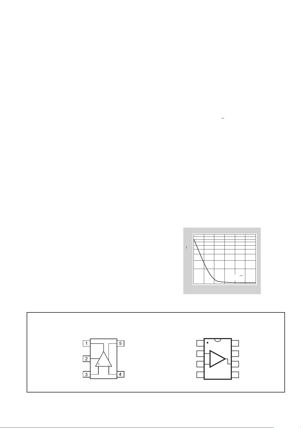
Pinout
SOT23-5
-
+
1
2
3
4
NC
V
inv
V
non-inv
-V
cc
R
p
(optional)
+V
cc
V
out
NC
8
7
6
5
Pinout
DIP & SOIC
CLC425 Electrical Characteristics (V
CC
= ±5V; A
V
= +20; R
f
=499
ΩΩ
ΩΩ
Ω; R
g
= 26.1
ΩΩ
ΩΩ
Ω; R
L
= 100
ΩΩ
ΩΩ
Ω; unless noted)
PARAMETERS CONDITIONS TYP MIN/MAX RATINGS UNITS SYMBOL
Ambient Temperature CLC425 AJ +25
°
C -40°C +25°C +85°C
FREQUENCY DOMAIN RESPONSE
gain bandwidth product V
out
< 0.4V
pp
1.9 1.5 1.5 1.0 GHz GBW
-3dB bandwidth V
out
< 0.4V
pp
95 75 75 50 MHz SSBW
V
out
< 5.0V
pp
40 30 30 20 MHz LSBW
gain flatness V
out
< 0.4V
pp
peaking DC to 30MHz 0.3 0.7 0.5 0.7 dB GFP
rolloff DC to 30MHz 0.1 0.7 0.5 0.7 dB GFR
linear phase deviation DC to 30MHz 0.7 1.5 1.5 2.5 ° LPD
TIME DOMAIN RESPONSE
rise and fall time 0.4V step 3.7 4.7 4.7 7.0 ns TRS
settling time to 0.2% 2V step 22 30 30 40 ns TSS
overshoot 0.4V step 5 12 10 12 % OS
slew rate 2V step 350 250 250 200 V/µsSR
DISTORTION AND NOISE RESPONSE
2
nd
harmonic distortion 1Vpp, 10MHz - 53 48 48 46 dBc HD2
3rd harmonic distortion 1Vpp, 10MHz - 75 65 65 60 dBc HD3
3
rd
order intermodulation intercept 10MHz 35 dBm IMD
equivalent noise input
voltage 1MHz to 100MHz 1.05 1.25 1.25 1.8 nV/√Hz VN
current 1MHz to 100MHz 1.6 4.0 2.5 2.5 pA/√Hz ICN
noise figure R
S
= 700Ω 0.9 dB NF
STATIC DC PERFORMANCE
open-loop gain DC 96 77 86 86 dB AOL
*input offset voltage ± 100 ±1000 ± 800 ± 1000 µV VIO
average drift ± 2 8
____
4 µV/°C DVIO
*input bias current 12 40 20 20 µAIB
average drift - 100 - 250
____
- 120 nA/°C DIB
input offset current ± 0.2 3.4 2.0 2.0 µA IIO
average drift ± 3 ± 50
____
± 25 nA/°C DIIO
power supply rejection ratio DC 95 82 88 86 dB PSRR
common mode rejection ratio DC 100 88 92 90 dB CMRR
*supply current R
L
= ∞ 15 18 16 16 mA ICC
MISCELLANEOUS PERFORMANCE
input resistance common-mode 2 0.6 1.6 1.6 MΩ RINC
differential-mode 6 1 3 3 kΩ RIND
input capacitance common-mode 1.5 2 2 2 pF CINC
differential-mode 1.9 3 3 3 pF CIND
output resistance closed loop 5 50 10 10 mΩ ROUT
output voltage range R
L
= ∞ ±3.8 ±3.5 ±3.7 ±3.7 V VO
R
L
=100Ω ±3.4 ±2.8 ±3.2 ±3.2 V VOL
input voltage range common mode ± 3.8 ±3.4 ± 3.5 ± 3.5 V CMIR
output current source 80 70 70 70 mA IOP
sink 80 45 55 55 mA ION
Min/max ratings are based on product characterization and simulation. Individual parameters are tested as noted. Outgoing quality levels are
determined from tested parameters.
http://www.national.com 2
Absolute Maximum Ratings Miscellaneous Ratings
V
cc
±7V
I
out
short circuit protected to ground, however maximum reliabiliy
is obtained if I
out
does not exceed... 125mA
common-mode input voltage ±V
cc
maximum junction temperature +150°C
operating temperature range:
AJ -40°C to +85°C
storage temperature range -65°C to +150°C
lead temperature (soldering 10 sec) +300°C
ESD (human body model) 1000V
Recommended gain range ±10 to ±1,000V/V
Notes:
* AJ :100% tested at +25°C.
Pac kage Thermal Resistance
Package
θθ
θθ
θ
JC
θθ
θθ
θ
JA
AJP 70°C/W 125°C/W
AJE 65°C/W 145°C/W
A8B 45°C/W 135°C/W
AJM5 115°C/W 185°C/W
Reliability Information
Transistor count 31
3 http://www.national.com

(µA)
http://www.national.com 4

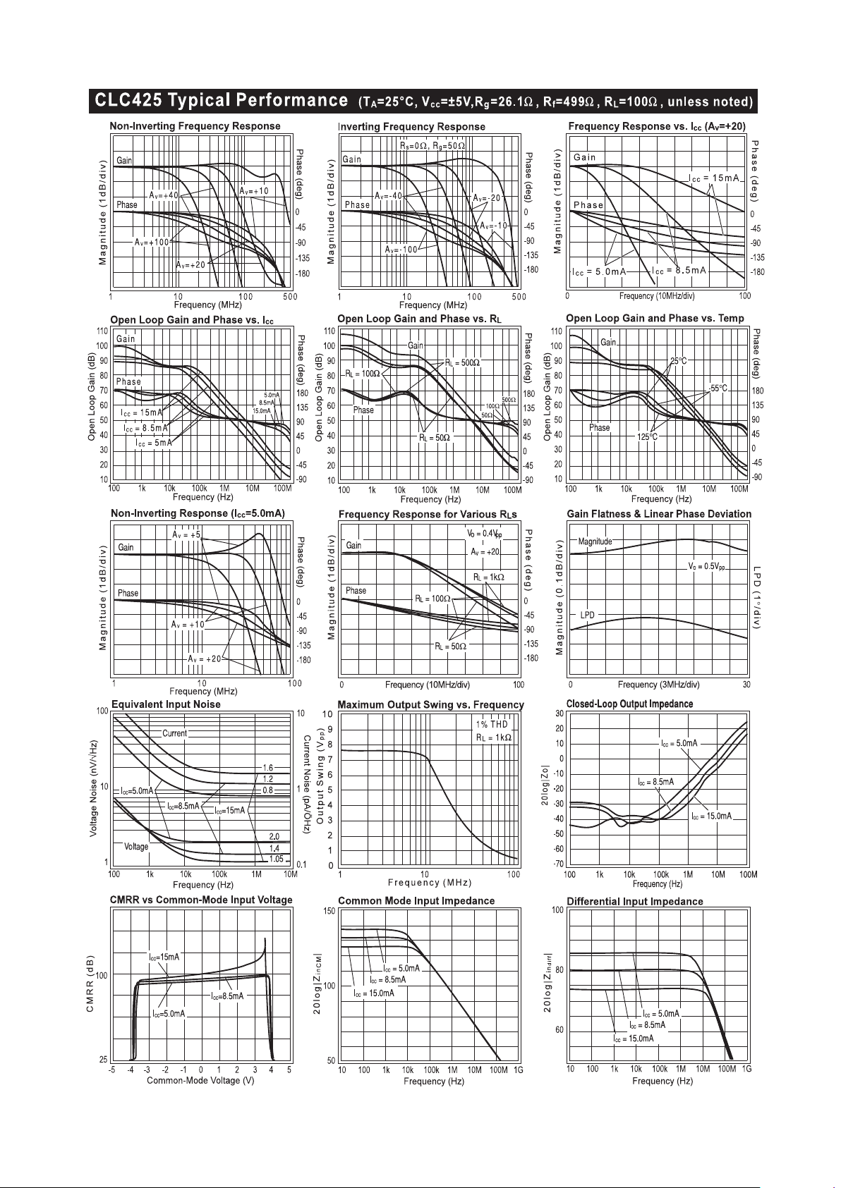
Introduction
The CLC425 is a very wide gain-bandwidth, ultra-low
noise voltage feedback operational amplifier which enables application areas such as medical diagnostic ultrasound, magnetic tape & disk storage and fiber-optics to
achieve maximum high-frequency signal-to-noise ratios.
The set of characteristic plots located in the "Typical
Performance" section illustrates many of the performance trade-offs. The following discussion will enable
the proper selection of external components in order to
achieve optimum device performance.
Bias Current Cancellation
In order to cancel the bias current errors of the noninverting configuration, the parallel combination of the
gain-setting (Rg) and feedback (Rf) resistors should equal
the equivalent source resistance (R
s
eq
) as defined in
Figure 1. Combining this constraint with the non-inverting gain equation also seen in Figure 1, allows both R
f
and Rg to be determined explicitly from the following
equations: Rf=AvR
s
eq
and Rg=Rf/(Av-1). When driven from
a 0Ω source, such as that from the output of an op amp,
the non-inverting input of the CLC425 should be isolated
with at least a 25Ω series resistor.
As seen in Figure 2, bias current cancellation is accomplished for the inverting configuration by placing a resistor (Rb) on the non-inverting input equal in value to the
resistance seen by the inverting input (Rf||(Rg+Rs)). Rb is
recommended to be no less than 25Ω for best CLC425
performance. The additional noise contribution of Rb can
be minimized through the use of a shunt capacitor.
4 16 4 21 25kT e Joules C=− °. @
R
f
3
2
4
7
6
R
g
0.1µF
0.1µF
6.8µF
6.8µF
-V
cc
+V
cc
V
out
R
T
R
s
eq
=
R
s
|| R
T
R
f
R
g
Av= 1 +
V
s
V
in
R
s
CLC425
R
f
R
g
CLC425
R
s
eq
e
n
i
n
+
i
n
-
√4kTR
g
√4kTR
f
√4kTR
s
eq
Total Input Noise vs. Source Resistance
In order to determine maximum signal-to-noise ratios
from the CLC425, an understanding of the interaction
between the amplifier's intrinsic noise sources and the
noise arising from its external resistors is necessary.
Figure 3 describes the noise model for the non-inverting
amplifier configuration showing all noise sources. In
addition to the intrinsic input voltage noise (en) and
current noise (in=in+=in-) sources, there also exists thermal voltage noise (
e
4TR
t
=
k
) associated with each of
the external resistors. Equation 1 provides the general
form for total equivalent input voltage noise density (eni).
Equation 2 is a simplification of Equation 1 that assumes
Rf||Rg = R
s
eq
for bias current cancellation. Figure 4
illustrates the equivalent noise model using this assumption. Figure 5 is a plot of eni against equivalent
source resistance (R
s
eq
) with all of the contributing voltage noise sources of Equation 2 shown. This plot gives
the expected eni for a given R
s
eq
which assumes Rf||Rg =
R
s
eq
for bias current cancellation. The total equivalent
output voltage noise (eno) is eni∗Av.
Equation 1: General Noise Equation
e e i R kTR i R R kT R R
ni n n
ss
n
f
g
f
g
eq eq
=+
()
++
()
()
+
()
+−
2
2
2
44|| ||
Figure 3: Non-inverting Amplifer Noise Model
Figure 1: Non-inverting Amplifier Configuration
Figure 4: Noise Model with Rf||Rg = R
s
eq
R
f
3
2
4
7
6
R
g
0.1µF
0.1µF
6.8µF
6.8µF
-V
cc
+V
cc
V
out
V
s
V
in
R
b
R
s
Av= -
R
f
R
g
CLC425
e
n
A
v
2R
s
eq
√4kT2R
s
eq
i
n
√2
Equation 2: Noise Equation with Rf||Rg = R
s
eq
e e i R kT R
ni n n s s
eq eq
=+
()
+
()
2
2
242
Figure 2: Inverting Amplifier Configuration
5 http://www.national.com

As seen in Figure 5, eni is dominated by the intrinsic
voltage noise (en) of the amplifier for equivalent source
resistances below 33.5Ω. Between 33.5Ω and 6.43kΩ,
eni is dominated by the thermal noise (
e
4TR
t
seq
=
k
) of
the external resistors. Above 6.43kΩ, eni is dominated by
the amplifier's current noise (
2i R
n seq
). The point at
which the CLC425's voltage noise and current noise
contribute equally occurs for R
s
eq
=464Ω (i.e.
e2i
nn
/
).
As an example, configured with a gain of +20V/V giving
a -3dB of 90MHz and driven from an R
s
eq
=25Ω, the
CLC425 produces a total equivalent input noise voltage
(
e 1.57 90MHz
ni
∗∗
) of 16.5µV
rms
.
Figure 5: Voltage Noise Density vs. Source Resistance
If bias current cancellation is not a requirement, then
Rf||Rg does not need to equal R
s
eq
. In this case, according
to Equation 1, Rf||Rg should be as low as possible in
order to minimize noise. Results similar to Equation 1
are obtained for the inverting configuration of Figure 2 if
R
s
eq
is replaced by Rb and Rg is replaced by Rg+Rs. With
these substitutions, Equation 1 will yield an eni refered to
the non-inverting input. Refering eni to the inverting input
is easily accomplished by multiplying eni by the ratio of
non-inverting to inverting gains.
Noise Figure
Noise Figure (NF) is a measure of the noise degradation
caused by an amplifier.
The Noise Figure formula is shown in Equation 3. The
addition of a terminating resistor RT, reduces the
external thermal noise but increases the resulting NF.
The NF is increased because RT reduces the input signal
amplitude thus reducing the input SNR.
R
seq
= Rs for Unterminated Systems
R
seq
= Rs II RT for Terminated Systems
Equation 3: Noise Figure Equation
The noise figure is related to the equivalent source
resistance (R
s
eq
) and the parallel combination of Rf and
Rg. To minimize noise figure, the following steps are
recommended:
• Minimize Rf||R
g
• Choose the optimum Rs (R
OPT
)
R
OPT
is the point at which the NF curve reaches a
minimum and is approximated by:
R
OPT
≅ (en/in)
Figure 6 is a plot of NF vs Rs with Rf||Rg = 9.09 (Av = +10).
The NF curves for both Unterminated and Terminated
systems are shown. The Terminated curve assumes R
s
= RT. The table indicates the NF for various source
resistances including Rs = R
OPT
.
Figure 6: Noise Figure vs Source Resistance
Supply Current Adjustment
The CLC425's supply current can be externally adjusted
downward from its nominal value by adding an optional
resistor (Rp) between pin 8 and the negative supply as
shown in Figure 7. Several of the plots found within the plot
pages demonstrate the CLC425’s behavior at different
supply currents. The plot labeled “Icc vs. Rp” provides the
means for selecting Rp and shows the result of standard IC
process variation which is bounded by the 25°C curve.
Figure 7: External Supply Current Adjustment
Non-Inverting Gains Less Than 10V/V
Using the CLC425 at lower non-inverting gains requires
external compensation such as the shunt compensation
as shown in Figure 8. The quiescent supply current must
also be reduced to 5mA with Rp for stability. The compensation capacitors are chosen to reduce frequency
response peaking to less than 1dB. The plot in the
"Typical Performance" section labeled “Differential Gain
and Phase” shows the video performance of the CLC425
with this compensation circuitry.
3
2
4
7
6
8
+V
cc
-V
V
out
R
p
CLC425
NF 10LOG
S/N
S/N
10LOG
e
e
ii
oo
ni
2
t
2
=
=
NF 10LOG
e i R R ||R 4kTR 4kT R | | R
4kTR
n2n2seq f g
2
seq f g
seq
=
++
()
++
()
http://www.national.com 6

Inverting Gains Less Than 10V/V
The lag compensation of Figure 9 will achieve stability
for lower gains. Placing the network between the two
input terminals does not affect the closed-loop nor noise
gain, but is best used for the invering configuration
because of its affect on the non-inverting input impedance.
Single-Supply Operation
The CLC425 can be operated with single power supply
as shown iin Figure 10. Both the input and output are
capacitively coupled to set the dc operating point.
Low Noise Transimpedance Amplifier
The circuit of Figure 11 implements a low-noise transimpedance amplifier commonly used with photo-diodes.
The transimpedance gain is set by Rf. The simulated
frequency response is shown in Figure 12 and shows
the influence Cf has over gain flatness. Equation 4
provides the total input current noise density (ini) equation for the basic transimpedance configuration and is
plotted against feedback resistance (Rf) showing all
contributing noise sources in Figure 13. This plot indicates the expected total equivalent input current noise
density (ini) for a given feedback resistance (Rf). The total
equivalent output voltage noise density (eno) is ini∗Rf.
Very Low Noise Figure Amplifier
The circuit of Figure 14 implements a very low Noise
Figure amplifier using a step-up transformer combined
with a CLC425 and a CLC404. The circuit is configured
with a gain of 35.6dB. The circuit achieves measured
Noise Figures of less than 2.5dB in the 10-40MHz
region. 3rd order intercepts exceed +30dBm for frequencies less than 40MHz and gain flatness of 0.5dB is measured
in the 1-50MHz pass bands. Application Note OA-14 provides
greater detail on these low Noise Figure techniques.
R
f
R
b
CLC425
+V
cc
C
f
Figure 11: Transimpedance Amplifier Configuration
AIR
vin
f
=− ∗
R
f
=
124Ω
R
s
=
75Ω
R
g
=
124Ω
CLC425
R
in
C
in
39pF
C
f
=
10pF
I
cc
=5mA
75Ω
75Ω
75Ω
Figure 8: External Shunt Compensation
Figure 12: Transimpedance Amplifier Frequency Response
R
g
R
f
R
b
R
L
CLC425
R
V
out
R
out
V
in
C
7 http://www.national.com
Figure 9: External Lag Compensation
R
f
R
R
L
R
out
C
C
C
R
R
g
V
ac
V
cc
V
cc
CLC425
V
cc
2
V
cc
2
+ AvV
ac
V
out
=
Figure 10: Single Supply Operation
Equation 4: Total Equivalent Input Refered Current
ii
ni n
n
ff
e
R
kT
R
=+ +
2
2
4
Figure 13: Current Noise Density vs. Feedback Resistance

20Ω
200Ω
600Ω
50Ω
50Ω
40kΩ
50kΩ
180Ω
20Ω
10Ω
P
i
Mini-Circuits
T16-6T
P
o
Av=+10
A
v
=-3
806Ω
50Ω
1:4
CLC425
CLC404
0.1µF
1pF
Gain =
P
o
P
i
= 35.6dB
Figure 14: Very Low Noise Figure Amplifier
R
f
=
1kΩ
R
1
=
45.3Ω
R
=
681Ω
R
g
=
50ΩR
2
=
200Ω
V
o
V
in
CLC425
L
=
0.1µHC
=
470pF
C
1
=
2200pF
V
V
sC R
sC R R
R
RR
sLR
s LCR R sL R R R R
o
in
o
f
f
g
g
ggg
K=
+
+
()
+
−
+
++
()
+
11
11
2
222
1
1
VV
K
sR C
K
R
R
oin
o
a
o
f
g
≅=+;1
R
RRRR
RR
b
a
f
g
a
||
,≥>>
R
f
R
b
R
a
R
g
V
o
V
in
CLC425
R
C
50Ω
50Ω
R
f
R
g
CLC425
R
1
R
2
C
2
C
1
Figure 17: Low Noise Magnetic Media Equalizer
K
R
R
o
f
g
=+1
R
f
R
b
R
g
CLC425
V
in
V
out
C
f
Figure 18: Equalizer Frequency Response
Low-Noise Phase-Locked Loop Filter
The CLC425 is extremely useful as a Phase-Locked
Loop filter in such applications as frequency synthesizers and data synchronizers. The circuit of Figure 19
implements one possible PLL filter with the CLC425.
Figure 19: Phased-Locked Loop Filter
Decreasing the Input Noise Voltage
The input noise voltage of the CLC425 can be reduced
from its already low 1.05nV/√Hz by slightly increasing the
supply current. Using a 50kΩ resistor to ground on pin 8,
as shown in the circuit of Figure 14, will increase the
quiescent current to ≈17mA and reduce the input noise
voltage to < 0.95nV/√Hz.
Printed Circuit Board Layout
Generally, a good high-frequency layout will keep power
supply and ground traces away from the inverting input
and output pins. Parasitic capacitances on these nodes
to ground will cause frequency response peaking and
possible circuit oscillation, see OA-15 for more information. National suggests the CLC730013-DIP,
CLC730027-SOIC, or CLC730068-SOT evaluation
board as a guide for high-frequency layout and as an aid
in device testing and characterization.
Low Noise Integrator
The CLC425 implements a deBoo integrator shown in
Figure 15. Integration linearity is maintained through
positive feedback. The CLC425's low input offset
voltage and matched inputs allowing bias current
cancellation provide for very precise integration. Stability is maintained through the constraint on the circuit
elements.
Figure 15: Low Noise Integrator
High-Gain Sallen-Key Active Filters
The CLC425 is well suited for high-gain Sallen-Key type
of active filters. Figure 16 shows the 2nd order Sallen-Key
low pass filter topology. Using component predistortion
methods as discussed in OA-21 enables the proper
selection of components for these high-frequency filters.
Figure 16: Sallen-Key Active Filter Topology
Low Noise Magnetic Media Equalizer
The CLC425 implements a high-performance low-noise
equalizer for such applications as magnetic tape
channels as shown in Figure 17. The circuit combines an
integrator with a bandpass filter to produce the lownoise equalization. The circuit's simulated frequency
response is illustrated in Figure 18.
http://www.national.com 8

CLC425
Ultra Low Noise Wideband Op Amp
http://www.national.com
12
Customer Design Applications Support
National Semiconductor is committed to design excellence. For sales, literature and technical support, call the
National Semiconductor Customer Response Group at 1-800-272-9959 or fax 1-800-737-7018.
Life Support Policy
National’s products are not authorized for use as critical components in life support devices or systems without the express written approval
of the president of National Semiconductor Corporation. As used herein:
1. Life support devices or systems are devices or systems which, a) are intended for surgical implant into the body, or b) support or
sustain life, and whose failure to perform, when properly used in accordance with instructions for use provided in the labeling, can
be reasonably expected to result in a significant injury to the user.
2. A critical component is any component of a life support device or system whose failure to perform can be reasonably expected to
cause the failure of the life support device or system, or to affect its safety or effectiveness.
National Semiconductor National Semiconductor National Semiconductor National Semiconductor
Corporation Europe Hong Kong Ltd. Japan Ltd.
1111 West Bardin Road Fax: (+49) 0-180-530 85 86 2501 Miramar Tower Tel: 81-043-299-2309
Arlington, TX 76017 E-mail: europe.support.nsc.com 1-23 Kimberley Road Fax: 81-043-299-2408
Tel: 1(800) 272-9959 Deutsch Tel: (+49) 0-180-530 85 85 Tsimshatsui, Kowloon
Fax: 1(800) 737-7018 English Tel: (+49) 0-180-532 78 32 Hong Kong
Francais Tel: (+49) 0-180-532 93 58 Tel: (852) 2737-1600
Italiano Tel: (+49) 0-180-534 16 80 Fax: (852) 2736-9960
National does not assume any responsibility for use of any circuitry described, no circuit patent licenses are implied and National reserves the right at any time without notice to change said
circuitry and specifications.
 Loading...