NSC CLC416AJE-TR13, CLC416AJE-TR, CLC416AJE, CLC416AJP Datasheet

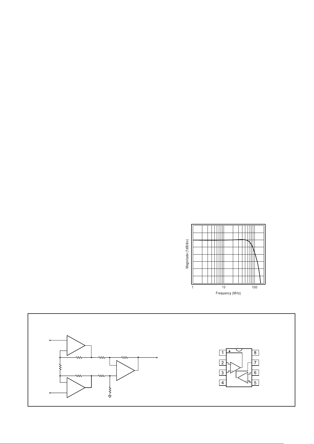
Typical Application Diagram
Instrumentation Amplifier
Pinout
DIP & SOIC
CLC416
Dual Low-Power, 120MHz Op Amp
September 1998
Features
■
0.01%, 0.03° DG, Dφ
■
Very low input bias current: 100nA
■
High input impedance: 6MΩ
■
120MHz -3dB bandwidth (Av= +2)
■
Low power
■
High output current: 60mA
■
Low-cost
Applications
■
Desktop video systems
■
Video distribution
■
Flash A/D driver
■
High-speed driver
■
High-source impedance applications
■
Professional video processing
■
High resolution monitors
General Description
The CLC416 is a dual, wideband (120MHz) op amp. The
CLC416 consumes only 39mW per channel and can source or
sink an output current of 60mA. These features make the
CLC416 a versatile, high-speed solution for demanding
applications that are sensitive to both power and cost.
Utilizing National’s proven architectures, this dual current
feedback amplifier surpasses the performance of alternative
solutions and sets new standards for low power. This powerconserving dual op amp achieves low distortion with -80dBc and
-80dBc second and third harmonics respectively. Many high
source impedance applications will benefit from the CLC416’s
6MΩ input impedance. And finally, designers will have a bipolar
part with an exceptionally low 100nA non-inverting bias current.
With 0.1dB flatness to 30MHz and low differential gain and phase
errors, the CLC416 is an ideal part for professional video
processing and distribution. The 120MHz -3dB bandwidth (Av=
+2) coupled with a 400V/µs slew rate also makes the CLC416
a perfect choice in cost-sensitive applications such as video
monitors, fax machines, copiers, and CATV systems.
Vo1
V
inv
1
V
non-inv
1
-V
CC
Vo2
V
inv
2
V
non-inv
2
+V
CC
+
-
348Ω
1/2
CLC416
R
1
348Ω
-
+
1/2
CLC416
348Ω
348Ω
V
out
= 3(V2 - V1)
348Ω
348Ω
348Ω
-
+
CLC405
V
1
V
2
Frequency Response (Av = +2V/V)
CLC416
Dual Low-Power, 120MHz Op Amp
N
© 1998 National Semiconductor Corporation http://www.national.com
Printed in the U.S.A.

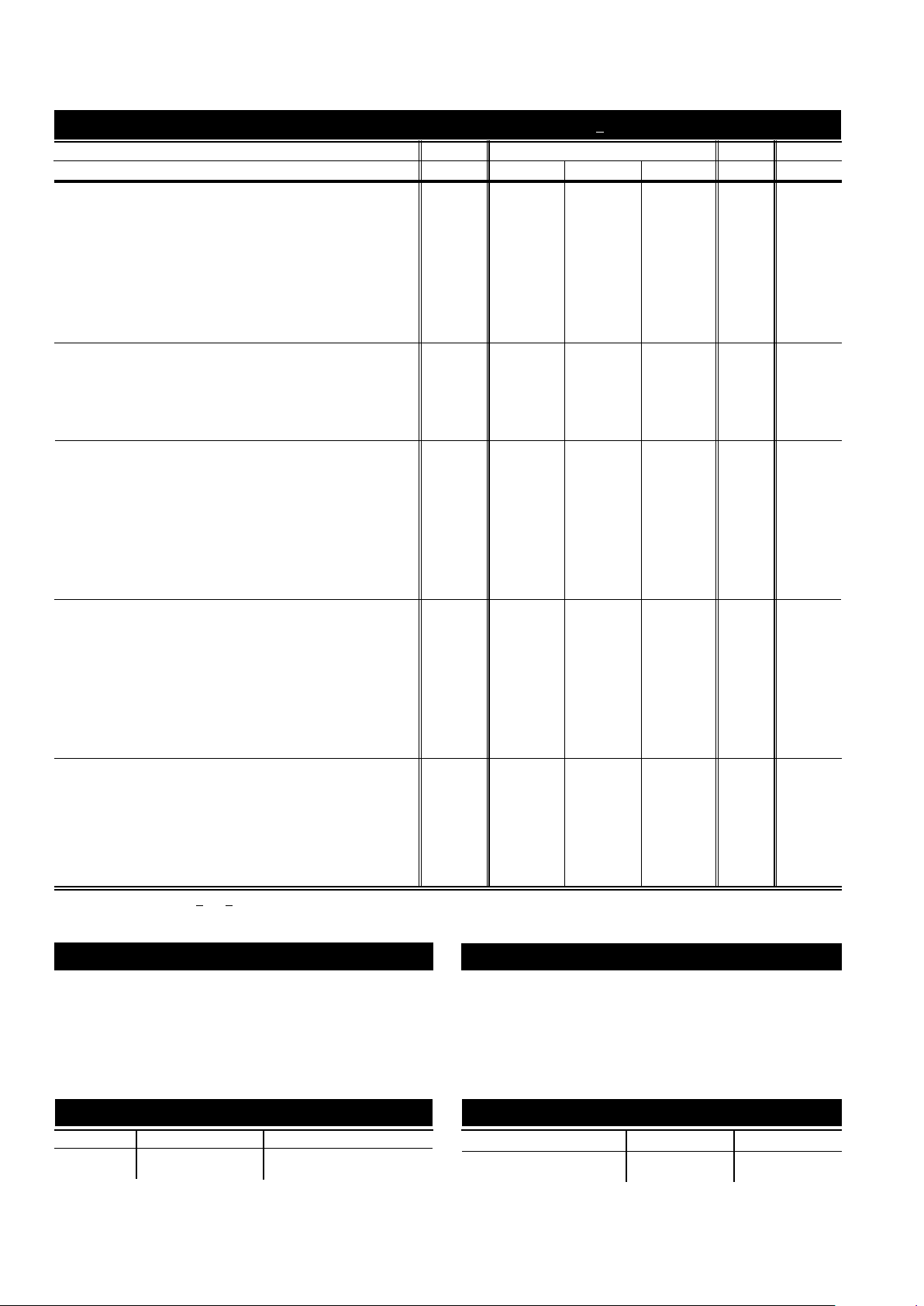
PARAMETERS CONDITIONS TYP MIN/MAX RATINGS UNITS NOTES
Ambient Temperature CLC416AJ +25˚C +25˚C 0 to 70˚C -40 to 85˚C
FREQUENCY DOMAIN RESPONSE
-3dB bandwidth V
out
< 1.0V
pp
120 65 45 45 MHz
V
out
< 5.0V
pp
52 40 36 35 MHz 1
±
0.1dB bandwidth V
out
< 1.0V
pp
30 15 MHz
gain flatness V
out
< 1.0V
pp
peaking DC to 200MHz 0.1 0.7 0.8 1.0 dB
rolloff <30MHz 0 0.3 0.6 0.6 dB
linear phase deviation <20MHz 0.3 0.6 0.7 0.7 deg
differential gain 4.43MHz, R
L
=150Ω 0.01 0.04 0.04 0.04 %
differential phase 4.43MHz, R
L
=150Ω 0.03 0.08 0.11 0.12 deg
TIME DOMAIN RESPONSE
rise and fall time 2V step 4.3 6.5 7.2 7.4 ns
settling time to 0.05% 2V step 22 30 38 41 ns
overshoot 2V step 3 12 12 12 %
slew rate A
V
= +2 2V step 400 300 260 250 V/µs
A
V
= -1 1V step 700 V/µs
DISTORTION AND NOISE RESPONSE
2
nd
harmonic distortion 2Vpp, 1MHz -80 dBc
3
rd
harmonic distortion 2Vpp, 1MHz -80 dBc
2
nd
harmonic distortion 2Vpp, 10MHz -65 -55 -50 -47 dBc
3
rd
harmonic distortion 2Vpp, 10MHz -57 -50 -45 -45 dBc
equivalent input noise
voltage >1MHz 5 6.3 6.6 6.7 nV/√Hz
inverting current >1MHz 12 15 16 17 pA/√Hz
non-inverting current >1MHz 3 3.8 4.0 4.2 pA/√Hz
crosstalk, input referred 2V
pp
, 10MHz 72 66 66 66 dB
STATIC DC PERFORMANCE
input offset voltage 1 5 7 8 mV A
average drift 30 50 50 µV/˚C
input bias current non-inverting 100 900 1600 2800 nA A
average drift 3 8 11 nA/˚C
input bias current inverting 1 5 6 8 µAA
average drift 17 40 45 nA/˚C
power supply rejection ratio DC 52 47 47 45 dB
common-mode rejection ratio DC 50 45 45 43 dB
supply current per channel R
L
= ∞ 3.9 4.5 4.6 4.9 mA A
MISCELLANEOUS PERFORMANCE
input resistance non-inverting 6 3 2.4 1 MΩ
input capacitance non-inverting 1 2 2 2 pF
common mode input range
±
2.2 ±1.8 ±1.7 ±1.5 V
output voltage range R
L
= 100Ω +3.5,-2.9 +3.1/-2.8 +2.9/-2.7 +2.4/-1.7 V
output voltage range R
L
= ∞ +4.0,-3.4 +3.9/-3.3 +3.8/-3.2 +3.7/-2.8 V
output current 60 44 38 20 mA
output resistance, closed loop 0.06 0.2 0.25 0.4 Ω
Recommended gain range +1 to +40V/V Transistor count = 110
Min/max ratings are based on product characterization and simulation. Individual parameters are tested as noted. Outgoing quality levels are
determined from tested parameters.
CLC416 Electrical Characteristics
(AV= +2, Rf= 348Ω: Vcc= + 5V, RL= 100Ω unless specified)
Absolute Maximum Ratings
supply voltage
±
7V
I
out
is short circuit protected to ground
common-mode input voltage
±
Vcc
maximum junction temperature +175˚C
storage temperature range -65˚C to +150˚C
lead temperature (soldering 10 sec) +300˚C
ESD rating (human body model) 1000V
Notes
1) At temps < 0˚C, spec is guaranteed for RL= 500Ω.
A) J-level: spec is 100% tested at +25˚C.
Ordering Information
Model Temperature Range Description
CLC416AJP -40˚C to +85˚C 8-pin PDIP
CLC416AJE -40˚C to +85˚C 8-pin SOIC
Package Thermal Resistance
Package θ
JC
θ
JA
Plastic (AJP) 80°C/W 95°C/W
Surface Mount (AJE) 95°C/W 115°C/W
http://www.national.com 2
 Loading...