

NSC 5962-9457901VXA, 5962-9457901MYA, 5962-9457901MXA, 100351W-QMLV, 100351MW8 Datasheet
100351
Low Power Hex D Flip-Flop
General Description
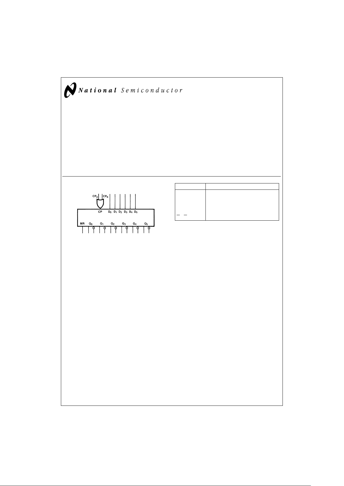
The 100351 contains six D-type edge-triggered, master/
slave flip-flops with true and complement outputs, a pair of
common Clock inputs (CP
a
and CPb) and common Master
Reset (MR) input. Data enters a master when both CP
a
and
CP
b
are LOW and transfers to the slave when CPaand CP
b
(or both) go HIGH. The MR input overrides all other inputs
and makes the Q outputs LOW. All inputs have 50 kΩ
pull-down resistors.
Features
n 40%power reduction of the 100151
n 2000V ESD protection
n Pin/function compatible with 100151
n Voltage compensated operating range:
−4.2V to −5.7V
n Standard Microcircuit Drawing
(SMD) 5962-9457901
Logic Symbol
Pin Names Description
D
0–D5
Data Inputs
CP
a
,CP
b
Common Clock Inputs
MR Asynchronous Master Reset Input
Q
0–Q5
Data Outputs
Q
0–Q5
Complementary Data Outputs
DS100318-11
August 1998
100351 Low Power Hex D Flip-Flop
© 1998 National Semiconductor Corporation DS100318 www.national.com
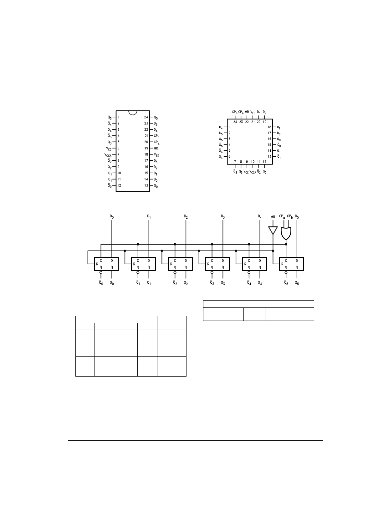
Connection Diagrams
Logic Diagram
Truth Tables
(Each Flip-flop)
Synchronous Operation
Inputs Outputs
D
n
CP
a
CP
b
MR Qn(t+1)
L
N
LL L
H
N
LL H
LL
N
LL
HL
N
LH
XH
N
LQ
n
(t)
X
N
HL Q
n
(t)
XL LL Q
n
(t)
Asynchronous Operation
Inputs Outputs
D
n
CP
a
CP
b
MR Qn(t+1)
XX XH L
H
=
HIGH Voltage Level
L=LOW Voltage Level
X=Don’t Care
t=Time before CP positive transition
t+1=Time after CP positive transition
N
=
LOW-to-HIGH transition
24-Pin DIP
DS100318-1
24-Pin Quad Cerpak
DS100318-2
DS100318-4
www.national.com 2

Absolute Maximum Ratings (Note 1)
If Military/Aerospace specified devices are required,
please contact the National Semiconductor Sales Office/
Distributors for availability and specifications.
Above which the useful life may be impaired
Storage Temperature (T
STG
) −65˚C to +150˚C
Maximum Junction Temperature (T
J
)
Ceramic +175˚C
V
EE
Pin Potential to Ground Pin −7.0V to +0.5V
Input Voltage (DC) V
EE
to +0.5V
Output Current (DC Output HIGH) −50 mA
ESD (Note 2) ≥2000V
Recommended Operating
Conditions
Case Temperature (TC)
Military −55˚C to +125˚C
Supply Voltage (V
EE
) −5.7V to −4.2V
Note 1: Absolute maximum ratings are those values beyond which the device may be damaged or have its useful life impaired. Functional operation
under these conditions is not implied.
Note 2: ESD testing conforms to MIL-STD-883, Method 3015.
Military Version
DC Electrical Characteristics
V
EE
=
−4.2V to −5.7V, V
CC
=
V
CCA
=
GND, T
C
=
−55˚C to +125˚C
Symbol Parameter Min Max Units T
C
Conditions Notes
V
OH
Output HIGH Voltage −1025 −870 mV 0˚C to V
IN
=
V
IH
(Max)
or V
IL
(Min)
Loading with
50Ω to −2.0V
(Notes 3, 4, 5)
+125˚C
−1085 −870 mV −55˚C
V
OL
Output LOW Voltage −1830 −1620 mV 0˚C to
+125˚C
−1830 −1555 mV −55˚C
V
OHC
Output HIGH Voltage −1035 mV 0˚C to V
IN
=
V
IH
(Min)
or V
IL
(Max)
Loading with
50Ω to −2.0V
(Notes 3, 4, 5)
+125˚C
−1085 mV −55˚C
V
OLC
Output LOW Voltage −1610 mV 0˚C to
+125˚C
−1555 mV −55˚C
V
IH
Input HIGH Voltage −1165 −870 mV −55˚C to Guaranteed HIGH Signal (Notes 3, 4, 5, 6)
+125˚C for All Inputs
V
IL
Input LOW Voltage −1830 −1475 mV −55˚C to Guaranteed LOW Signal (Notes 3, 4, 5, 6)
+125˚C for All Inputs
I
IL
Input LOW Current 0.50 µA −55˚C to V
EE
=
−4.2V (Notes 3, 4, 5)
+125˚C V
IN
=
V
IL
(Min)
I
IH
Input HIGH Current V
EE
=
−5.7V
V
IN
=
V
IH
(Max)
(Notes 3, 4, 5)
CP, MR 350 µA 0˚C to
D
0–D5
240 +125˚C
CP, MR 500 µA −55˚C
D
0–D5
340
I
EE
Power Supply Current −135 −50 mA −55˚C to Inputs Open (Notes 3, 4, 5)
+125˚C
Note 3: F100K 300 Series coldtemperaturetesting is performed by temperature soaking (to guarantee junction temperature equals −55˚C), then testing immediately
without allowing for the junction temperature to stabilize due to heat dissipation after power-up. This provides “cold start” specs which can be considered a worst case
condition at cold temperatures.
Note 4: Screen tested 100%on each device at −55˚C, +25˚C, and +125˚C, Subgroups 1, 2, 3, 7, and 8.
Note 5: Sample tested (Method 5005, Table I) on each manufactured lot at −55˚C, +25˚C, and +125˚C, Subgroups A1, 2, 3, 7, and 8.
Note 6: Guaranteed by applying specified input condition and testing V
OH/VOL
.
3 www.national.com
 Loading...