NSC CLC411MDC, CLC411AJP, CLC411AJE-TR13, CLC411AJE, 5962-9456601MPA Datasheet

N
CLC411
High-Speed Video Op Amp with Disable
General Description
The CLC411 combines a state-of-the-art complementary bipolar
process with National’s patented current-feedback architecture to
provide a very high-speed op amp operating from ±15V supplies.
Drawing only 11mA quiescent current, the CLC411 provides a
200MHz small signal bandwidth and a 2300V/µs slew rate while
delivering a continuous 70mA current output with ±4.5V output swing.
The CLC411’s high-speed performance includes a 15ns settling time
to 0.1% (2V step) and a 2.3ns rise and fall time (6V step).
The CLC411 is designed to meet the requirements of professional
broadcast video systems including composite video and high definition
television. The CLC411 exceeds the HDTV standard for gain flatness
to 30MHz with it's ±0.05dB flat frequency response and exceeds
composite video standards with its very low differential gain and
phase errors of 0.02%, 0.03°. The CLC411 is the op amp of choice
for all video systems requiring upward compatibility from NTSC and
PAL to HDTV.
The CLC411 features a very fast disable/enable (10ns/55ns) allowing
the multiplexing of high-speed signals onto an analog bus through the
common output connections of multiple CLC411’s. Using the same
signal source to drive disable/enable pins is easy since “breakbefore-make” is guaranteed.
The CLC411 is available in several versions:
CLC411AJP -40°C to +85°C 8-pin plastic DIP
CLC411AJE -40°C to +85°C 8-pin plastic SOIC
CLC411A8B -55°C to +125°C 8-pin hermetic CERDIP,
MIL-STD-883
CLC411AMC -55°C to +125°C dice, MIL-STD-883, Level B
DESC SMD number: 5962-94566
June 1999
CLC411
High-Speed Video Op Amp with Disable
Features
■ 200MHz small signal bandwidth (1V
pp
)
■ ±0.05dB gain flatness to 30MHz
■ 0.02%, 0.03° differential gain, phase
■ 2300V/µs slew rate
■ 10ns disable to high-impedance output
■ 70mA continuous output current
■ ±4.5V output swing into 100Ω load
■ ±4.0V input voltage range
Applications
■ HDTV amplifier
■ Video line driver
■ High-speed analog bus driver
■ Video signal multiplexer
■ DAC output buffer
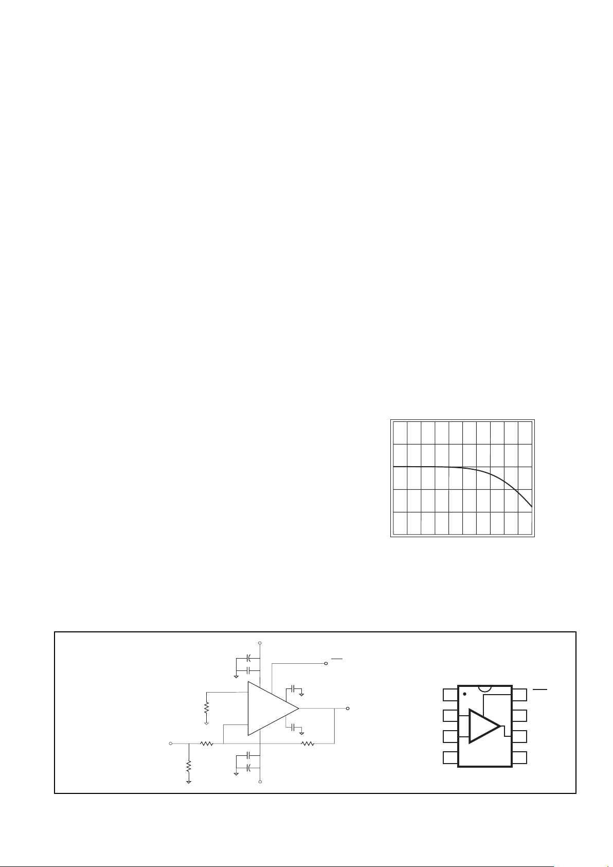
Pinout
DIP & SOIC
0.01µF
0.1µF
0.1µF
6.8µF
6.8µF
0.01µF
+V
r
-V
r
V
in
+
_
3
2
4
7
8
1
5
6
CLC411
25Ω
R
T
R
g
Select RTto yield
Rin=RT||R
g
R
f
V
out
DIS
-V
cc
+V
cc
Recommended
Inverting Gain
Configuration
0 Frequency (5MHz/div) 50
Magnitude (0.5dB/div)
Gain Flatness (Av=+2)
-
+
1
2
3
4
DIS
+V
cc
V
out
-V
r
+V
r
V
inv
V
non-inv
-V
cc
8
7
6
5
1999 National Semiconductor Corporation http://www.national.com
Printed in the U.S.A.

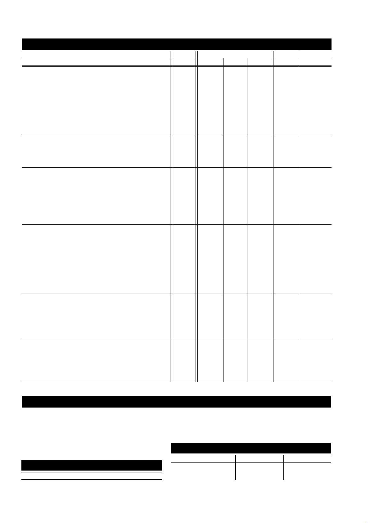
PARAMETERS CONDITIONS TYP MIN/MAX RATINGS UNITS SYMBOL
Ambient Temperature CLC411 AJ +25
°
C -40°C +25°C +85°C
FREQUENCY DOMAIN RESPONSE
-3dB bandwidth V
out
< 1V
pp
20 0 15 0 150 110 MH z SSBW
V
out
< 6V
pp
75 50 50 40 MHz LSBW
gain flatness V
out
< 1V
pp
peaking DC to 30MHz 0.05 0.2 0.2 0.3 dB GFPL
rolloff DC to 30MHz 0.05 0.2 0.2 0.4 dB GFRL
peaking DC to 200MHz 0.1 0. 6 0.5 0. 6 d B GFPH
rolloff DC to 60MHz 0.2 0.7 0.4 0. 7 d B GFRH
linear phase deviation DC to 60MHz 0.3 1.0 1.0 1.0 ° LPD
differential gain 4.43MHz, R
L
=150W 0.02 % DG
differential phase 4.43MHz, RL=150W 0.03 ° DP
TIME DOMAIN RESPONSE
rise and fall time 6V step 2 .3 ns TR
settling time to 0.1% 2V step 15 23 18 23 ns TS
overshoot 2V step 5 15 10 15 % OS
slew rate 6V step 23 00 V/µsSR
DISTORTION AND NOISE RESPONSE (note 1)
2
ND
harmonic distortion 2Vpp, 20MHz -48 -35 -35 -35 dBc HD2
3
RD
harmonic distortion 2Vpp, 20MHz -52 -42 -42 -35 dBc HD3
equivalent noise input
voltage >1MHz 2.5 nV/√Hz VN
inverting current >1MHz 12.9 pA/√Hz ICI
non-inverting current >1MHz 6.3 pA/√Hz ICN
noise floor >1MHz -157 dBm
1Hz
SNF
integrated noise 1MHz to 200MHz 45 µVINV
STATIC DC PERFORMANCE
*input offset voltage ±2 ±13 ±9.0 ±1 4 mV VIO
average temperature coefficient +30 ± 50
____
±50 µV/°C DVIO
*input bias current non-inverting 12 65 30 ±20 µAIBN
average temperature coefficient ±200 ±400
____
±250 nA/°C DIBN
*input bias current inverting ±1 2 ±40 ±30 ±30 µA IBI
average temperature coefficient ±50 ±200
____
±150 nA/°C DIBI
power supply rejection ratio 56 48 50 48 dB PSRR
common mode rejection ratio 52 44 46 44 dB CMRR
*supply current no load 1 1 14 12 12 mA ICC
supply current disabled 2.5 4.5 3.5 4.5 mA ICCD
DISABLE/ENABLE PERFORMANCE (note 2)
disable time to >50dB attenuation @10MHz 10 3 0 30 60 ns TOFF
enable time 55 ns TON
DIS voltage pin 8
to disable 4.5 <3.0 <3.0 <3.0 V VDIS
to enable 5.5 >7.0 >6.5 >6.5 V VEN
off isolation at 10MHz 59 5 5 5 5 55 dB OSD
MISCELLANEOUS PERFORMANCE
non-inverting input resistance 100 0 250 7 50 1000 kΩ RIN
non-inverting input capacitance 2.0 3.0 3.0 3.0 pF CIN
output voltage range no load ±6.0 ±4.5 V VO
output voltage range R
L
=100Ω ±4.5 ±4.0 V VOL
common mode input range ±4.0 ±3.5 V CMIR
output current 70 30 50 40 mA IO
Min/max ratings are based on product characterization and simulation. Individual parameters are tested as noted. Outgoing quality levels
are determined from tested parameters.
CLC411 Electrical Characteristics
(A(A
(A(A
(A
VV
VV
V
= +2; V= +2; V
= +2; V= +2; V
= +2; V
CCCC
CCCC
CC
= =
= =
=
±±
±±
±
15V; R15V; R
15V; R15V; R
15V; R
LL
LL
L
= 100= 100
= 100= 100
= 100
ΩΩ
ΩΩ
Ω
; R; R
; R; R
; R
ff
ff
f
= 301= 301
= 301= 301
= 301
ΩΩ
ΩΩ
Ω
, unless noted), unless noted)
, unless noted), unless noted)
, unless noted)
Absolute Maximum Ratings
Miscellaneous Ratings
V
cc
±18V
I
out
125mA
common-mode input voltage ±V
cc
differential input voltage ±15V
maximum junction temperature +150°C
operating temperature range: AJ -40°C to +85°C
storage temperature range -65°C to +150°C
lead temperature (soldering 10 sec) +300°C
ESD (human body model) 1000V
Recommended gain range ±1 to ±10V/V
Notes: * AJ :100% tested at +25°C.
note 1 : Specifications guaranteed using 0.01mF bypass capacitors
on pins 1 & 5.
note 2 : Break before make is guaranteed.
http://www.national.com 2
Package Thermal Resistance
Package
θθ
θθ
θ
JC
θθ
θθ
θ
JA
AJP 65°C/W 120°C/W
AJE 55°C/W 135°C/W
A8B 25°C/W 115°C/W
Reliability Information
Transistor count 70

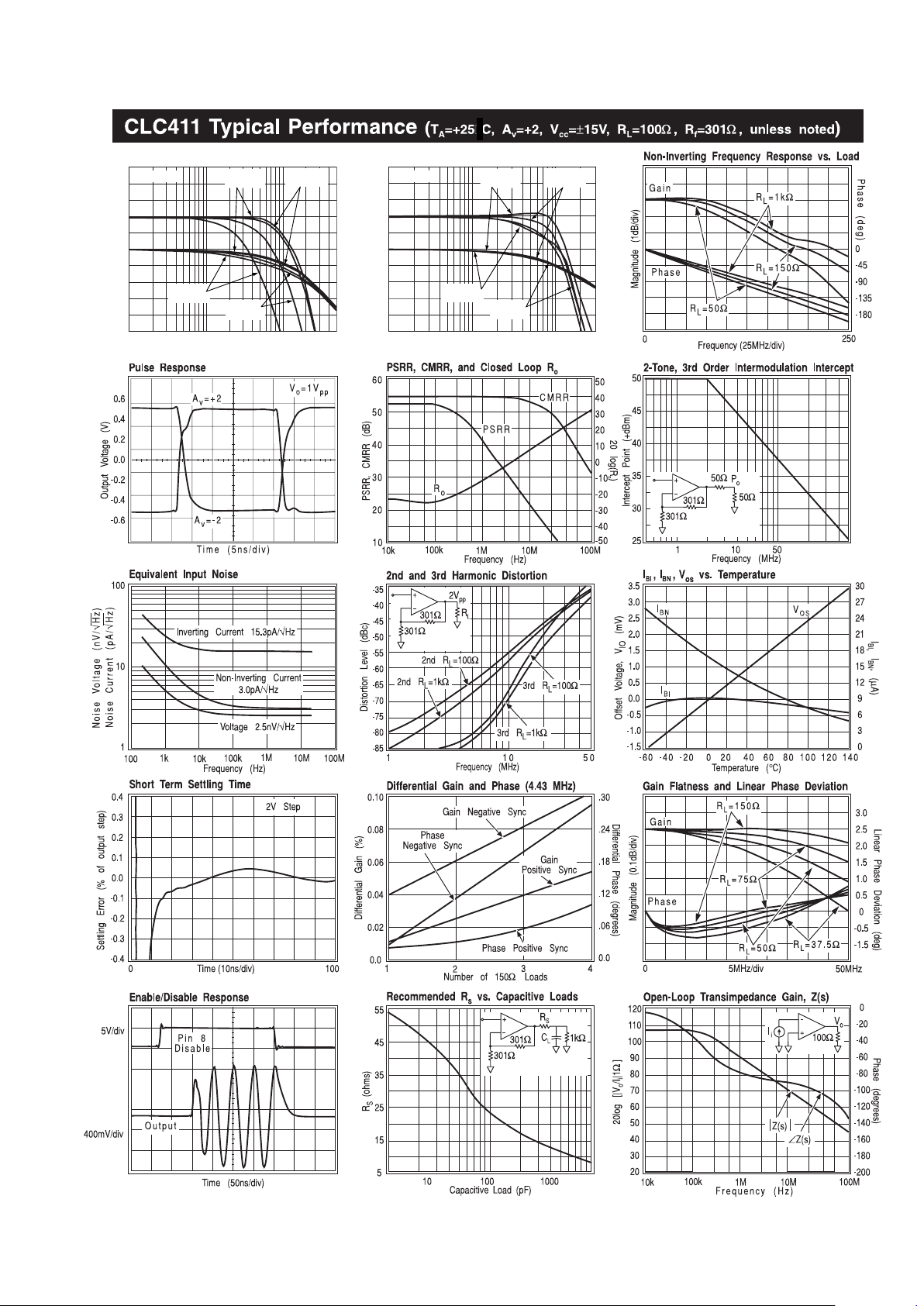
Inverting Frequency Response
Magnitude (1dB/div)
Frequency (MHz)
1
10
100
Phase (deg)
-270
-540
-360
-450
-180
-630
V
out
= 1V
pp
Av = -2
Rf = 301Ω
Av = -1
Rf = 301Ω
Av = -10
Rf = 200Ω
Av = -5
Rf = 249Ω
Non-Inverting Frequency Response
Magnitude (1dB/div)
Frequency (MHz)
1
10
100
Phase (deg)
-90
-360
-180
-270
0
-450
V
out
= 1V
pp
Av = 2
Rf = 301Ω
Av = 1
R
f
= 402Ω
Av = 10
Rf = 200Ω
Av = 5
Rf = 200Ω
Frequency (MHz)
Frequency (MHz)
o
3 http://www.national.com
 Loading...