NOVATEK NT7704H-BDT, NT7704H-TABF4 Datasheet
240 Output LCD Segment/Common Driver
Features
(Segment mode)
Shift Clock frequency:
!
20 MHz (Max.) (V
12 MHz (Max.) (V
Adopts a data bus system
!
4-bit/8-bit parallel input modes are selectable with a
!
mode (MD) pin
Automatic transfer function with an enable signal
!
Automatic counting function when in "chip select" mode,
!
which causes the internal clock to be stopped by
automatically counting 240 bits of input data
(Common mode)
Shift clock frequency :
!
4.0 MHz (Max.)
Built-in 240-bits bidirectional shift register (divisible into
!
120-bits x 2)
General Description
The NT7704 is a 240-bit output segment/common driver LSI
suitable for driving large scale dot matrix LCD panels used
by PDA's, personal computers and work stations for
example. Through the use of COG technology, it is ideal for
substantially decreasing the size of the frame section of the
LCD module. The NT7704 is good as both a segment driver
and as a common driver, and a low power consuming, high-
= 5 V ± 10%)
DD
= 2.5V - 4.5V)
DD
Available in a single mode (240-bits shift register) or in a
!
NT7704
dual mode(120-bits shift register x 2)
1. Y1 → Y240 Single mode
2. Y240 → Y1 Single mode
3. Y1 → Y120, Y121 → Y240 Dual mode
4. Y240 → Y121, Y120 → Y1 Dual mode
The above 4 shift directions are pin-selectable
(Both for segment mode and common mode)
Supply voltage for LCD driver: 15.0 to 30.0 V
!
Number of LCD driver outputs: 240
!
Low output impedance
!
Low power consumption
!
Supply voltage for the logic system: +2.5 to +5.5 V
!
COMS process
!
Package: Gold bump die / 272 Pin TCP(Tape Carrier
!
Package)
Not designed or rated as radiation hardened
!
precision LCD panel display can be assembled using the
NT7704. In the segment mode, the data input is selected as
4bit parallel input mode or as 8bit parallel input mode by a
mode (MD) pin. In the common mode, the data input/output
pins are bi-directional and the four data shift directions are
pin-selectable.
Pin Configuration
D
Y
Y
Y
Y
U
2
M
4
M
0
Y
Y
2
2
2
2
3
3
3
3
9
8
7
6
270 269 268272
Y
Y
1
1
2
2
2
3
Y
Y
Y
Y
1
1
1
1
1
1
2
2
8
9
0
1
152153154155 150 34
Y5Y4Y3Y2Y
D
U
M
M
1
Y
353637271
33151
NT7704
123456789101112131415161718192021222324252627 28 29 30 31 32
D
U
M
M
Y
V
V
V
V
V
5
4
0
0
1
L
3
L
L
2
L
L
D0D1D2D3D4D5D6D7LPE
V
V
S
E
S
D
/
I
S
D
C
O
2
FRMDNCV
D
X
I
I
C
O
S
K
1
P
O
F
F
NCV
L
/
R
5
S
R
S
1V1.0
D
V
V
V
V
U
0
0
4
1
M
R
R
3
2
M
R
R
Y
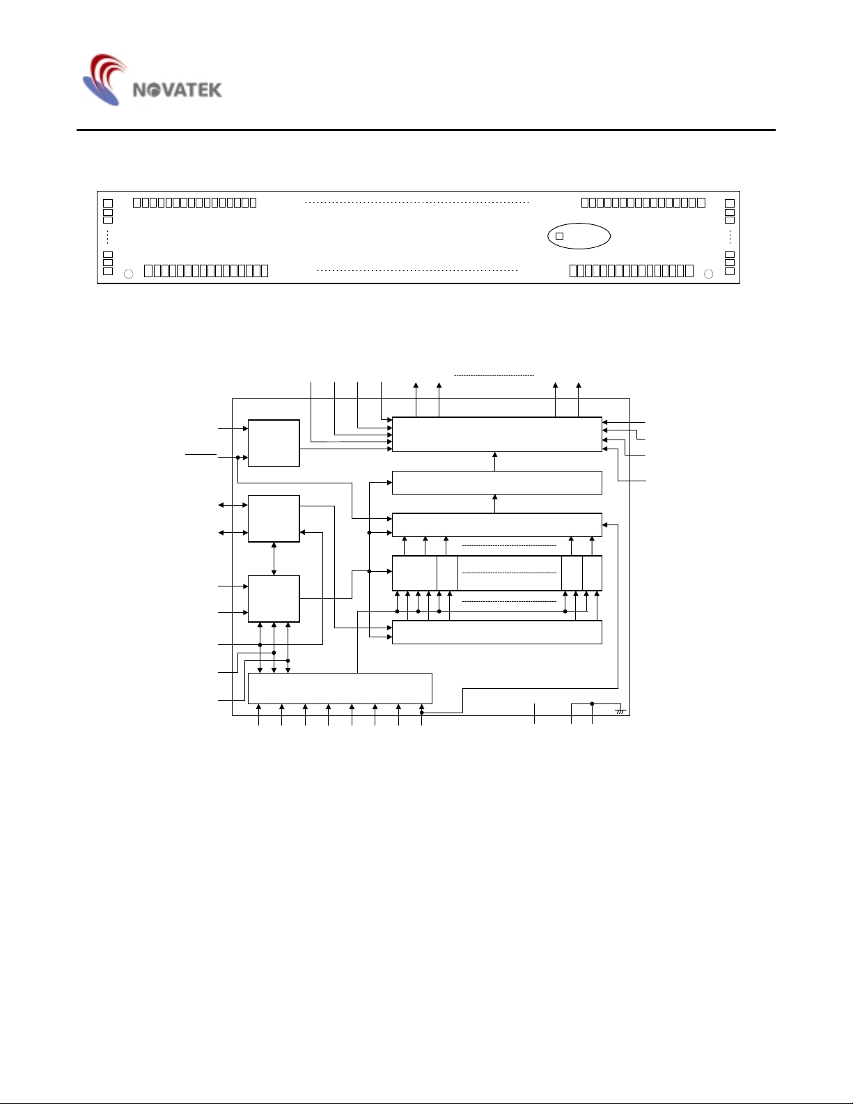
Pad Configuration
x
x
433
448
ALK_L
x
1
Block Diagram
NT7704
x
Dummy Pad
NT7704
225432
x
ALK_R
208
x
224
209
x
DISPOFF
EIO
EIO
XCK
L/R
MD
S/C
V
V
0R
FR
1
2
LP
Level
Shifter
Active
Control
Control
Logic
43R
12R
V
5R
Y1 Y2 Y239 Y240V
240 Bits 4 Level Driver
/240
240 Bits Level Shifter
/240
240 Bits Line Latch/Shift Register
8Bits2
Data
Latch
V
5L
43L
V
12L
V
0L
V
/16/16 /16 /16 /16
Data Latch Control
/8
SP Conversion & Data Control
(4 to 8 or 8 to 8)
D0D1D2D3D4D5D6D
7
V
VSSV
DD
SS
2

Pad Description
Pad No. Designation I/O Description
1 - 12 V
13 - 20 V
21 -28 V
29 - 40 V
41 - 66 V
67 - 92 V
0L
12L
43L
5L
SS
DD
93 - 94 S/C I Segment mode/common mode selection
95 - 97 EIO
2
P Power supply for LCD driver
P Power supply for LCD driver
P Power supply for LCD driver
P Power supply for LCD driver
P Ground (0V), these pads must be connected to each other
P Power supply for the logic system (+2.5 to +5.5V)
I/O Input/output for chip select or data of the shift register
NT7704
98, 99, 100 -
116, 117, 118
D0 - D6 I Display data input for segment mode
119 - 121 D7 I Display data input for Segment mode/ Dual mode data input
122 - 124 XCK I Display data shift clock input for segme nt mode
125 - 127
DISPOFF
I Control input for deselect output level
128 - 130 LP I Latch pulse input/shift clock input for the shift register
131 - 133 EIO
1
I/O Input/output for chip select or data of the shift register
134 - 136 FR I AC-converting signal input for LCD driver waveform
137 - 139 L/R I Display data shift direction selection
140 - 142 MD I Mode selection input
143 - 168 V
169 - 180 V
181 - 188 V
189 - 196 V
197 - 208 V
SS
5R
43R
12R
0R
P Ground (0V), these pads must be connected to each other
P Power supply for LCD driver
P Power supply for LCD driver
P Power supply for LCD driver
P Power supply for LCD driver
209 - 448 Y1 - Y240 O LCD driver output
3
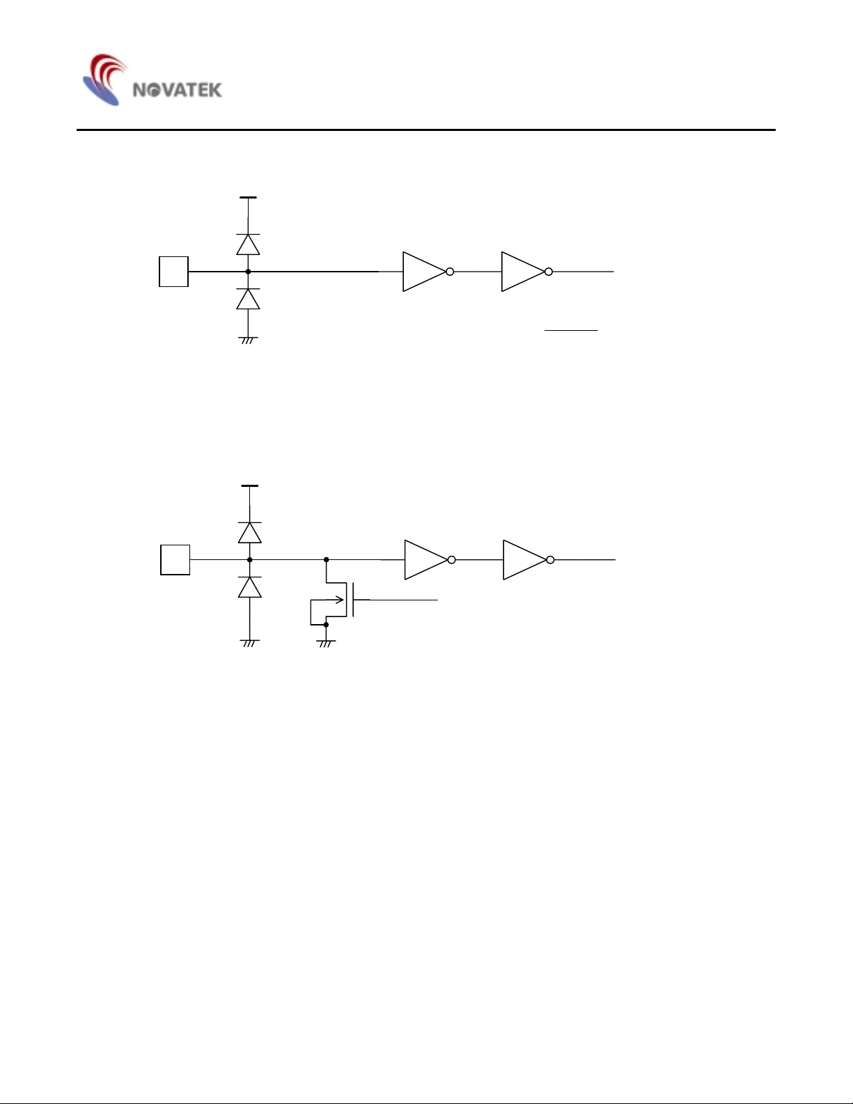
Input / Output Circuits
NT7704
DD
V
I
Input Signal
Applicable Pins
L/R, S/C, D0 - D6,
, LP, FR, MD
SS
V
Input Circuit (1)
DD
V
I
Control Signal
SS
V
SS
V
DISPOFF
Input Signal
Applicable Pins
D7, XCK
Input Circuit (2)
4
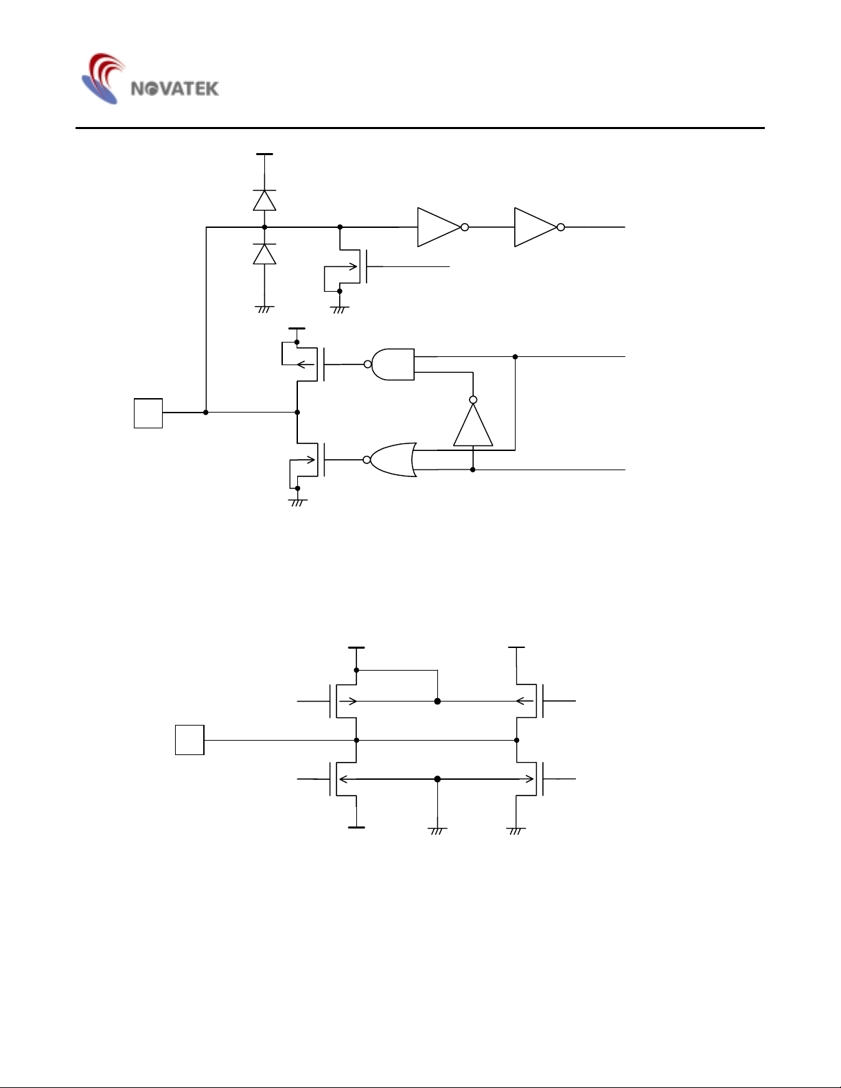
I/O
NT7704
DD
V
Input Signal
Control Signal
SS
V
DD
V
SS
V
SS
V
Output Signal
Control Signal
Applicable Pins
EIO1, EIO2
Control Signal 1
O
Control Signal 3
Input / Output Circuit
V0 V12
V43
SS
LCD Driver Output circuit
Control Signal 2
Control Signal 4
Applicable Pins
Y1 to Y240
V5V
5

Pad Description
Segment mode
Symbol Function
V
DD
V
SS
VOR, V
V
, V
12R
V
, V
43R
V5R, V
D
0 - D7
XCK
LP
L/R
DISPOFF
FR
MD
Logic system power supply pin connects from +2.5 to +5.5V
Ground pin connects to 0V
Power supply pin for LCD driver voltage bias
OL
12L
43L
5L
Normally, the bias voltage used is set by a resistor divider
"
Ensure that the voltages are set such that V
"
To further reduce the differences betw een the output w aveforms of the LCD driver outpu t pins Y1 and Y
"
externally connect ViR and V
(I = 0, 12, 43, 5)
iL
SS
V
≤
Input pin for display data
In 4-bit parallel input mode, input data into the 4 pins D
"
In 8-bit parallel input mode, input data into the 8 pins D0 - D
"
Clock input pin for taking display data
Data is read on the falling edge of the clock pulse
"
Latch pulse input pin for display data
Data is latched on the falling edge of the clock pulse
"
Direction selection pin for reading display data
When set to VSS level "L", data is read sequentially from Y240 to Y1
"
When set to VDD level "H", data is read sequentially from Y1 to Y240
"
Control input pin for output deselect level
The input signal is lev el-shifted from the logi c volta ge level to the LCD driver voltage level, and contro ls the
"
LCD driver circuit.
When set to V
"
When DISPOFF is set to “L”, the contents of the line latch are reset, but the display data in the data
"
latch are read regardless of the condition of
the driver outputs deselect level (V
falling edge of the LP. At that time, if the
level “L”, the LCD driver output pins (Y1-Y240) are set to level V
SS
DISPOFF. When the DISPOFF function is canceled,
or V43), then outputs the contents of the date latch onto the next
12
DISPOFF removal time can not keep regulation with what is
shown on the AC characteristics, then it can not output the reading data correctly.
AC signal input for LCD driving waveform
The input signal is level-shifted from the logic voltage level to the driver voltage level and controls
"
the LCD driver circuit.
It normally inputs a frame inversion signal
"
The LCD driver output pin’s output voltage level can be set to the line latch output signal and the FR signal
Mode selection pin
When set to VSS level “L”, 8-bit paral lel input mode is set
"
When set to VDD level “H", 4-bit parallel input mode is set
"
NT7704
< V
< V
5
43
0 - D3
< V
12
0
. Connect D4 - D7 to VSS or V
5
240,
DD
6

Segment mode continued
Symbol Function
Segment mode/common mode sele ctio n pin
When set to VDD level "H", segment mode is set
S/C
"
When set to V
"
level "L", common mode is set
SS
Input/output pin for chip selection
level “L”, EIO1 is set for output, and EIO2 is set for input
SS
XCK is “H” and then after 240-bits of data have been read,
EIO1, EIO
When L/R input is at V
"
When L/R input is at VDD level “H”, EIO1 is set for input, and EIO2 is set for output
"
2
During output, it is set to “H” while LP*
"
it is set to “L” for one cycle (from falling edge to falling edge of XCK), after which it returns to “H”
During input, after the LP signal is input, the chip is selected while EI is set to “L”. After 240-bits of
"
data have been read, the chip is deselected
LCD driver output pins
Y1 - Y
240
These correspond directly to each bit of the data latch, one level (V
output
Common mode
Symbol Function
NT7704
, V12, V43, or V5) is selected and
0
V
V
V0R, V
V
12R
V
43R
V5R, V
EIO
EIO
L/R
LP
DD
SS
, V
, V
1
2
0L
12L
43L
5L
Logic system power supply pin connects to +2.5 to +5.5V
Ground pin connects to 0V
Power supply pin for LCD driver voltage bias.
Normally, the bias voltage used is set by a resistor divider
"
< V
Ensure the voltages are set such that V
"
SS
V
≤
5 <V43
12
< V
0
To further reduce the differences between the output waveforms of the LCD driver output pins Y1 and
externally connect ViR and V
Y
240,
(I = 0, 12, 43, 5)
iL
Bi-directional shift register shift data input/output pin
Is an output pin when L/R is at V
"
When EIO
"
When EIO
"
is used as an input pin, it will be pulled-down
1
is used as an output pin, it won’t be pulled-down
1
level “L” and is an input pin when L/R is at VDD level “H”
SS
Bi-directional shift register shift data input/output pin
Is an input pin when L/R is at V
"
When EIO
"
When EIO
"
is used as an input pin, it will be pulled-down
2
is used as an output pin, it won’t be pulled-down
2
level “L” and is an output pin when L/R is at VDD level “H”
SS
Bi-directional shift register shift clock pulse input pin
Data is shifted on the falling edge of the clock pulse
"
Bi-directional shift register shift direction selection pin
Data is shifted from Y
"
set to V
level “H”
DD
to Y1 when it is set to VSS level “L”, and data i s shifted fr om Y1 to Y
240
when it is
240
7

Common mode continued
Symbol Function
DISPOFF
Control input pin for output deselect level
The input signal is level-shifted from the logic voltage level to the LCD driver voltage level, and controls
"
the LCD driver circuit
When set to V
"
While set to “L”, the contents of the s hift resister are reset a nd are no t reading data. When the
"
level “L”, the LCD driver output pins (Y1-Y
SS
function is canceled, the driver o utputs des elect lev el (V
edge of the LP. At that time, if the
DISPOFF removal time can not keep regulation with w hat is shown on
the AC characteristics, the shift data is not read correctly
FR AC signal input for LCD driving waveform
The input signal is level-sh ifted from lo gic volta ge level t o the LCD driver v oltage lev el, and it control s the
"
LCD driver circuit
Normally, it inputs a frame inversion signal
"
The LCD driver output pin’s outp ut voltage level can be set using the shift reg ister output si gnal and the FR
signal
MD Mode selection pin
When set to V
"
level “L”, Single Mode operation is selected. When set to VDD level “H”, Dual Mode
SS
operation is selected
D
7
Dual Mode data input pin
According to the data shift direction of the data shift re gister, data can be input starting from t he 121st bit
"
When the chip is used in Dual Mode, D
When the chip is used in Single Mode, D
will be pulled-down
7
won’t be pulled-down
7
S/C Segment mode/common mode selectio n pin
When set to V
"
level “L”, common mode is set
SS
D0 - D6 Not used
Connect D
"
to VSS or VDD. Avoid floating
0-D6
XCK Not used
XCK is pull-down in common mode, so connect to V
"
Y1 - Y
240
LCD driver output pins
These correspond directly to each bit of the shift register, one level (V
"
output
) are set to level V
240
or V43), and the shift data is re ad on the falling
12
or leave open
SS
, V
0
5
, or V5) is selected and
12, V43
NT7704
DISPOFF
8

Functional Description
1. Block description
1.1 Active Control
In segment mode, it controls the selection or deselection of
the chip. Following a LP signal input, and after the select
signal is input, a se lect signal is generated internally unti l 240
bits of data have been read in. Once data input has been
completed, a select signal for cascade connection is output,
and the chip is deselected.
In common mode, it controls the input/output data of the bidirectional pins.
1.2. SP Conversion & Data Control
In segment mode, it keeps input data which are 2 clocks of
XCK at 4-bit parallel mode into latch circuit, or keeps input
data which are 1 clock of XCK at 8-bit parallel mode into
latch circuit, after that they are put on t he i ntern al data bus 8
bits at a time.
1.3. Data Latch Control
In segment mode, it selec ts the state of the d ata latch, w hich
reads in the data bus signa ls. The sh ift dire ction i s contro lled
by the control logic and for every 16 bits of data read in, the
selection signal shifts one bit, based on the state of the
control circuit.
1.4. Data Latch
In segment mode, it latches the data on the data bus. The
latched state of each LCD driver output pin is controlled by
the control logic and the data latch control. 240 bits of data
are read in 20 sets of 8 bits.
NT7704
1.5. Line Latch/Shift Register
In segment mode, it ensures all 240 bits which have been
read into the data latch, are simult aneously latched on to the
falling edge of the LP signal, and output to the level shift
block.
In common mode, it shifts data from the data input pin on to
the falling edge of the LP signal.
1.6. Level Shifter
It ensures the logic voltage signal is level-shifted to the LCD
driver voltage level, and output to the driver block.
1.7. 4-Level Driver
It drives the LCD driver output pins from the line latch/shift
register data, selecting one of 4 levels (V
based on the S/C, FR and
1.8. Control Logic
Controls the operation of each block. In segment mode,
when an LP signal has been input, all blocks are reset and
the control logic waits f or the se lectio n sign al outpu t fro m the
active control block. Once the selection signal has been
output, operation of th e dat a l atc h and data transmission are
controlled, 240 bits of data are read in, and the chip is
deselected.
In common mode, it controls the direction of data shift.
DISPOFF signals.
, V12, V43, V5)
0
9
NT7704
2. LCD Driver Output Voltage Level
The relationship between the data bus signal, AC converted signal FR and LCD driver output voltage is as shown in the table
below:
2.1. Segment Mode
1 - Y240
)
Here, V
SS
FR Latch Data
LLH V
LHH V
HLH V
HHH V
XXL V
< V
< V
V
≤
5
43
< V0, H: V
12
(+2.5 to +5.5V), L: V
DD
DISPOFF
SS
Driver Output Voltage Level (Y
43
5
12
0
5
(0V), X: Don't care
2.2. Common Mode
Here, V
SS
FR Latch Data
DISPOFF
LLH V
LHH V
HLH V
HHH V
XXL V
< V
< V
V
≤
5
43
< V0, H: V
12
(+2.5 to +5.5V), L: V
DD
(0V), X: Don't care
SS
Driver Output Voltage Level (Y
43
0
12
5
5
1 - Y240
)
Note: There are two kinds of power supply (logic level voltage, LCD driver voltage) for the LCD driver. Please supply regular
voltage which is assigned by specification for each power pin.
That time "Don't care" should be fixed to "H" or "L", avoiding floating.
10
3. Relationship between the Display Data and Driver Output pins
3.1. Segment Mode:
(a) 4-bit Parallel Mode
NT7704
MD L/R EIO1EIO
H L Output Input
H H Input Output
(b) 8-bit Parallel Mode
MD L/R EIO1EIO
L L Output Input
L H Input Output
2
2
Data
Input
D
0
D
1
D
2
D
3
D
0
D
1
D
2
D
3
Data
Input
D
0
D
1
D
2
D
3
D
4
D
5
D
6
D
7
D
0
D
1
D
2
D
3
D
4
D
5
D
6
D
7
Number of Clock
60clock 59clock 58clcok ~ 3clock 2clock 1clock
Y1 Y5 Y9
Y2 Y6 Y10
Y3 Y7 Y11
Y4 Y8 Y12
Y240 Y236 Y232
Y239 Y235 Y231
Y238 Y234 Y230
Y237 Y233 Y229
~
~
~
~
~
~
~
~
Y229 Y233 Y237
Y230 Y234 Y238
Y231 Y235 Y239
Y232 Y236 Y240
Y12 Y8 Y4
Y11 Y7 Y3
Y10 Y6 Y2
Y9 Y5 Y1
Number of Clock
30clock 29clock 28clcok ~ 3clock 2clock 1clock
Y1 Y9 Y17 ~ Y217 Y225 Y233
Y2 Y10 Y18 ~ Y218 Y226 Y234
Y3 Y11 Y19 ~ Y219 Y227 Y235
Y4 Y12 Y20 ~ Y220 Y228 Y236
Y5 Y13 Y21 ~ Y221 Y229 Y237
Y6 Y14 Y22 ~ Y222 Y230 Y238
Y7 Y15 Y23 ~ Y223 Y231 Y239
Y8 Y16 Y24 ~ Y224 Y232 Y240
Y240 Y232 Y224 ~ Y24 Y16 Y8
Y239 Y231 Y223 ~ Y23 Y15 Y7
Y238 Y230 Y222 ~ Y22 Y14 Y6
Y237 Y229 Y221 ~ Y21 Y13 Y5
Y236 Y228 Y220 ~ Y20 Y12 Y4
Y235 Y227 Y219 ~ Y19 Y11 Y3
Y234 Y226 Y218 ~ Y18 Y10 Y2
Y233 Y225 Y217 ~ Y17 Y9 Y1
11
3.2. Common Mode
NT7704
MD L/R Data Transfer Direction EIO
L
(Single)
L (shift to left) Y240 to Y1 Output Input X
H (shift to right) Y1 to Y240 Input Output X
L (shift to left)
H
(Dual)
H (shift to right)
Here, L: VSS (0V), H: V
(+2.5V to +5.5V), X: Don't care
DD
Note: "Don't care" should be fixed to "H" or "L", avoiding floating.
Y240 to Y121
Y120 to Y1
Y1 to Y120
Y121 to Y240
EIO
1
2
D
7
Output Input Input
Input Output Input
12
 Loading...