NOVATEK NT7701H-BDT, NT7701H-TABF3 Datasheet
160 Output LCD Segment/Common Driver
Features
(Segment mode)
! Shift Clock frequency :
14 MHz (Max.) (V
8 MHz (Max.) (V
= 5V ± 10%)
DD
= 2.5V - 4.5V)
DD
! Adopts a data bus system
! 4-bit/8-bit parallel input modes are selectable with a
mode (MD) pin
! Automatic transfer function with an enable signal
! Automatic counting function when in the chip select
mode, causes the internal clock to be stopped by
automatically counting 160 bits of input data
(Common mode)
! Shift clock frequency:
4.0MHz (Max.)
! Built-in 160-bits bidirectional shift register (divisible into
80-bits x 2)
General Description
The NT7701 is a 160-bit output segment/common driver LSI
suitable for driving the large scale dot matrix LCD panels
used by PDA's, personal computers and work stations for
example. Through the use of SST (Super Slim TCP)
technology, it is ideal for substantially decreasing the size of
the frame section of the LCD module. The NT7701 is good
as both a segment driver and a common driver, and a low
NT7701
! Available in a single mode (160-bits shift register) or in a
dual mode (80-bits shift register x 2)
1. Y1 → Y160 Single mode
2. Y160 → Y1 Single mode
3. Y1 → Y80, Y81 → Y160 Dual mode
4. Y160 → Y81, Y80 → Y1 Dual mode
The above 4 shift directions are pin-selectable
(Both segment mode and common mode)
! Supply voltage for LCD drive: 15.0 to 30.0V
! Number of LCD driver outputs: 160
! Low output impedance
! Low power consumption
! Supply voltage for the logic system: +2.5 to +5.5V
! COMS process
! Package : 190pin TCP (Tape Carrier Package)
! Not designed or rated as radiation hardened
power consuming, high-precision LCD panel display can be
assembled using the NT7701. In the segment mode, the
data input is selected 4bit parallel input mode or as 8bit
parallel input mode by a mode (MD) pin. In common mode,
the data input/output pins are bi-directional and the four data
shift directions are pin-selectable.
Pin Configuration
D
D
D
U
U
Y
Y
M
M
1
1
M
M
5
6
Y
Y
9
0
Y
Y
Y
Y
1
1
1
1
5
5
5
5
5
6
7
8
188 187 186 185190
Y
Y
Y
Y
Y
8
8
3
2
Y
8
8
7
7
1
0
9
8
109
110111112113 108 32
Y6Y5Y4Y3Y2Y
33343536189
D
U
U
M
M
M
M
Y
Y
1
31
NT7701
1
23456789101112131415161718192021222324252627282930
D
V
V
V
V
V
L
V
S
E
S
/
D
S
R
D
D0D1D2D3D4D5D6D7X
/
I
C
O
2
U
0
1
4
5
M
L
2
3
L
M
L
L
Y
D
LPE
FRMDT
I
C
S
K
P
O
F
F
T
I
E
E
O
S
S
1
T
T
1
2
1 V2.0
D
V
V
V
V
V
U
S
5
4
1
O
M
S
R
3
2
R
M
R
R
Y
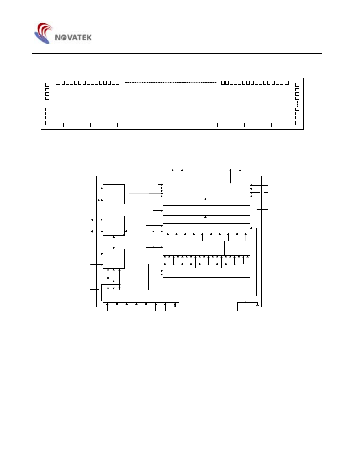
Pad Configuration
200
NT7701
54199
53
NT7701
216
1 36
Block Diagram
DISPOFF
EIO
EIO
XCK
L/R
MD
S/C
37
43R
12R
0R
V
V
V
FR
1
2
LP
Level
Shifter
Active
Control
Control
Logic
5R
V
Y1 Y2 Y159 Y160
5R
V
160 Bits 4 Level Driver
/160
160 Bits Level Shifter
/160
160 Bits Line Latch/Shift Register
8Bits x 2
Data
Latch
5L
V
43L
V
12L
V
0L
V
/16/16 /16 /16 /16 /16 /16 /16 /16 /16
Data Latch Control
/8
SP Conversion & Data Control
(4 to 8 or 8 to 8)
DI0DI1DI2DI3DI4DI5DI6DI
7
2
DD
V
VSSV
SS

Pin Description
Pin No. Designation I/O Description
1 V0L P Power supply for LCD driver
NT7701
2 V
3 V
4 V5L P Power supply for LCD driver
5 VSS P Ground (0V), these two pads must be connected to each other
6 L/R I Display data shift direction selection
7 VDD P Power supply for the logic system (+2.5 to +5.5V)
8 S/C I Segment mode / common mode selection
9 EIO2 I/O Input / output for chip select or data of shift register
10 - 16 D0 - D6 I Display data input for segment mode
17 D7 I Display data input for Segment mode / Dual mode data input
18 XCK I Display data shift clock input for segment mode
19
20 LP I Latch pulse input/shift clock input for the shift register
21 EIO1 I/O Input / output for chip select or data of the shift register
22 FR I AC-converting signal input for LCD driver waveform
23 MD I Mode selection input
24 TEST1 I Test pin, no connection for user
P Power supply for LCD driver
12L
P Power supply for LCD driver
43L
DISPOFF
I Control input for deselect output level
25 TEST2 I Test pin, no connection for user
26 VSS P Ground (0V), these two pads must be connected to each other
27 V5R P Power supply for LCD driver
28 V
29 V
30 V0R P Power supply for LCD driver
31 - 190 Y1 - Y160 O LCD driver output
P Power supply for LCD driver
43R
P Power supply for LCD driver
12R
3

Pad Description
Pad No. Designation I/O Description
1, 2 L/R I Display data shift direction selection
3, 4 VDD P Power supply for the logic system (+2.5 to + 5.5V)
5, 6 S/C I Segment mode/common mode selection
7, 8 EIO2 I/O Input/output for chip select or data of shift register
9,10 - 21, 22 D0 - D6 I Display data input for segment mode
23, 24 D7 I Display data input for Segment mode / Dual mode data input
25, 26 XCK I Display data shift clock input for segment mode
NT7701
27, 28
29, 30 LP I Latch pulse input / shift clock input for the shift register
31, 32 EIO1 I/O Input/output for chip select or data of the shift register
33, 34 FR I AC-converting signal input for LCD driver waveform
35, 36 MD I Mode selection input
37, 38, VSS P Ground (0V), these two pads must be connected to each other
39, 40 V5R P Power supply for LCD driver
41, 42 V
43, 44 V
45, 46 V0R P Power supply for LCD driver
47 - 206 Y1 - Y160 O LCD driver output
207, 208 V0L P Power supply for LCD driver
209, 210 V
211, 212 V
213, 214 V5L P Power supply for LCD driver
215, 216 VSS P Ground (0V), these two pads must be connected to each other
DISPOFF
P Power supply for LCD driver
43R
P Power supply for LCD driver
12R
P Power supply for LCD driver
12L
P Power supply for LCD driver
43L
I Control input for deselect output level
4
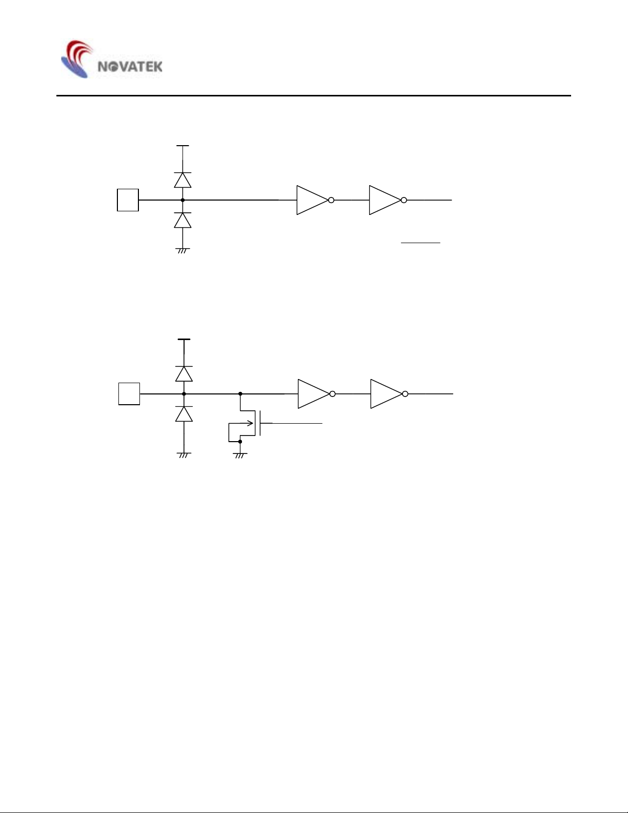
Input / Output Circuits
V
DD
NT7701
I
Input Signal
Applicable Pins
L/R, S/C, D0 - D6,
, LP, FR, MD
V
SS
Input Circuit (1)
V
DD
I
Control Signal
V
SS
V
SS
Input Circuit (2)
DISPOFF
Input Signal
Applicable Pins
D7, XCK
5
V
DD
NT7701
Input Signal
Control Signal
V
SS
V
DD
V
SS
Output Signal
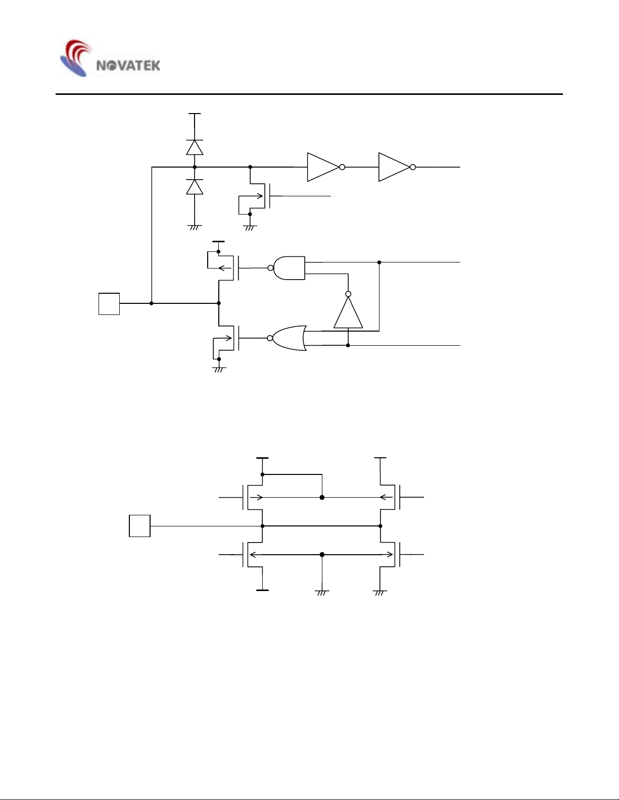
I/O
Control Signal
Applicable Pins
V
SS
EIO1, EIO2
Control Signal 1
O
Control Signal 3
Input / Output Circuit
V0 V12
V43
SS
LCD Driver Output circuit
Applicable Pins
Y1 to Y160
V5V
Control Signal 2
Control Signal 4
6

NT7701
Pad Description
Segment mode
Symbol Function
VDD Logic system power supply pin connects to +2.5 to +5.5V
VSS Ground pin connects to 0V
VOR, VOL
, V
12R
V
V
, V
43R
, V5L
5R
V
D0 - D7
XCK
LP
L/R
DISPOFF
FR
MD
Power supply pin for LCD driver voltage bias
# Normally, the bias voltage used is set by a resistor divider
12L
# Ensure that the voltages are set such that V
43L
# To further reduce the differences between the output waveforms of the LCD driver output pins Y
externally connect V
and V
iR
(I = 0, 12, 43)
iL
SS
≤ V
5
< V
43
< V
12
< V0
Input pin for display data
# In 4-bit parallel input mode, input data into the 4 pins D
# In 8-bit parallel input mode, input data into the 8 pins D
. Connect D4 - D7 to VSS or VDD
0 - D3
0 - D7
Clock input pin for taking display data
# Data is read on the falling edge of the clock pulse
Latch pulse input pin for display data
# Data is latched on the falling edge of the clock pulse
Direction selection pin for reading display data
# When set to VSS level "L", data is read sequentially from Y160 to Y1
# When set to V
level "H", data is read sequentially from Y1 to Y160
DD
Control input pin for output deselect level
# The input signal is level-shifted from logic voltage level to LCD driver voltage level, and controls LCD
driver circuit
# When set to V
# While
DISPOFF is set to “L”, the contents of the line latch are reset, but the display data in the data latch
are read regardless of the condition of
level “L”, the LCD driver output pins (Y1 - Yl60) are set to level V5
SS
DISPOFF . When the DISPOFF function is canceled, the driver
outputs deselect level (V12 or V43), then outputs the contents of the date latch onto the next falling edge
of the LP.
That time, if
DISPOFF removal time can not keep regulation what is shown AC characteristics, can not
output the reading data correctly
AC signal input for LCD driving waveform
# The input signal is level-shifted from the logic voltage level to the driver voltage level, and controls LCD
driver circuit
# Normally inputs a frame inversion signal
The LCD driver output pin’s output voltage level can be set to the line latch output signal and the FR signal
Mode selection pin
# When set to V
# When set to V
level “L”, 4-bit parallel input mode is set
SS
level “H", 8-bit parallel input mode is set
DD
and Y
1
160,
7

NT7701
Segment mode continued
Symbol Function
Segment mode/common mode selection pin
S/C
# When set to V
level "H", segment mode is set.
DD
# When set to VSS level "L", common mode is set.
Input/output pin for chip selection
# When L/R input is at VSS level “L”, EIO1 is set for output, and EIO2 is set for input.
EIO1, EIO2
# When L/R input is at V
# During output, it is set to “H” while LP*
level “H”, EIO1 is set for input, and EIO2 is set for output.
DD
XCK is “H” and after 160-bits of data have been read, it is set to
“L” for one cycle (from falling edge to falling edge of XCK), after which it returns to “H”
# During input, after the LP signal is input, the chip is selected while EI is set to “L”. After 160-bits of
data have been read, the chip is deselected
LCD driver output pins
Y1 - Y
160
These corresponding directly to each bit of the data latch, one level (V0, V12, V43, or V5) is selected and
output
Common mode
Symbol Function
VDD Logic system power supply pin connects to +2.5 to +5.5V
VSS Ground pin connects to 0V
V0R, V0L
V
, V
12R
, V
43R
V
V5R, V5L
12L
43L
Power supply pin for LCD driver voltage bias.
# Normally, the bias voltage used is set by a resistor divider
# Ensure that the voltages are set such that V
SS
≤ V
5 <V43
< V
12
< V0
# To further reduce the differences between the output waveforms of the LCD driver output pins Y
externally connect ViR and V
160,
Y
(I = 0, 12, 43)
iL
and
1
Bi-directional shift register shift data input/output pin
EIO1
# Is an Output pin when L/R is at V
# When EIO
# When EIO
is used as an input pin, it will be pulled-down
1
is used as an output pin, it won’t be pulled-down
1
level “L” and an input pin when L/R is at VDD level “H”
SS
Bi-directional shift register shift data input/output pin
EIO2
LP
# Is an Input pin when L/R is at V
# When EIO
# When EIO
is used as an input pin, it will be pulled-down
2
is used as an output pin, it won’t be pulled-down
2
Bi-directional shift register shift clock pulse input pin
# Data is shifted on the falling edge of the clock pulse
level “L” and an output pin when L/R is at VDD level “H”
SS
Bi-directional shift register shift direction selection pin
L/R
# Data is shifted from Y
level “H”
set to V
DD
to Y1 when it is set to VSS level “L”, and data is shifted from Y1 to Y
160
when it is
160
8

NT7701
Common mode continued
Symbol Function
Control input pin for output deselect level
# The input signal is level-shifted from the logic voltage level to the LCD driver voltage level and it controls
the LCD driver circuit
DISPOFF
# When set to V
# While set to “L”, the contents of the shift resister are reset and not reading data. When the
level “L”, the LCD driver output pins (Y1 - Y
SS
) are set to level V5
160
DISPOFF
function is canceled, the driver outputs deselect level (V12 or V34), and the shift data is read on the falling
edge of the LP. That time, if DISPOFF removal time can not keep regulation what is shown AC
characteristics, the shift data is not reading correctly
AC signal input for LCD driving waveform
# The input signal is level-shifted from the logic voltage level to the LCD driver voltage level, and controls the
FR
LCD driver circuit
# Normally, inputs a frame inversion signal
The LCD driver output pin’s output voltage level can be set using the shift register output signal and the FR
signal
Mode selection pin
MD
# When set to VSS level “L”, Single Mode operation is selected. When set to VDD level “H”, Dual Mode
operation is selected
Dual Mode data input pin
D7
S/C
D0 - D6
XCK
# According to the data shift direction of the data shift register, data can be input starting from the 81st bit
When the chip is used as Dual Mode, D
When the chip is used as Single Mode, D
will be pulled-down
7
won’t be pulled-down
7
Segment mode/common mode selection pin
# When set to VSS level “L”, common mode is set
Not used
# Connect D
to VSS or VDD. Avoiding floating
0-D6
Not used
# XCK is pulled-down in common mode, so connect to V
or open
SS
LCD driver output pins
Y1 - Y
160
# These corresponding directly Corresponding directly to each bit of the shift register, one level (V0, V
) is selected and output
5
or V
12, V43
,
9

Functional Description
1. Block description
1.1. Active Control
In the case of segment mode, controls the selection or
deselection of the chip. Following a LP signal input, and after
the select signal is input, a select signal is generated
internally until 160 bits of data have been read in. Once data
input has been completed, a select signal for cascade
connection is output, and the ship is deselected.
In the case of common mode, controls the input/output data
of bidirectional pins.
1.2. SP Conversion & Data Control
In the case of segment mode, keep input data which are 2
clocks of XCK at 4-bit parallel mode into latch circuit, or keep
input data which are 1 clock of XCK at 8-bit parallel mode
into latch circuit, after that they are put on the internal data
bus 8 bits at a time.
1.3. Data Latch Control
In the case of the segment mode, it selects the state of the
data latch, which reads in the data bus signals. The shift
direction is controlled by the control logic and for every 16
bits of data read in, the selection signal shifts one bit, based
on the state of the control circuit.
1.4. Data Latch
In the case of the segment mode, it latches the data on the
data bus. The latched state of each LCD driver output pin is
controlled by the control logic and the data latch control 160
bits of data are read in 20 sets of 8 bits.
NT7701
1.5. Line Latch / Shift Register
In the case of the segment mode, all 160 bits which have
been read into the data latch, are simultaneously latched on
to the falling edge of the LP signal, and output to the level
shift block.
In the case of the common mode, shifts data from the data
input pin on to the falling edge of the LP signal.
1.6. Level Shifter
The logic voltage signal is level-shifted to the LCD driver
voltage level, and output to the driver block.
1.7. 4-Level Driver
It drives the LCD driver output pins from the line latch/shift
register data, selecting one of 4 levels (V
based on the S/C, FR and DISPOFF signals.
1.8. Control Logic
It controls the operation of each block. In the case of the
segment mode, when an LP signal has been input, all blocks
are reset and the control logic waits for the selection signal
output from the active control block. Once the selection
signal has been output, operation of the data latch and data
transmission are controlled, 160 bits of data are read in, and
the chip is deselected.
In the case of the common mode, it controls the direction of
the data shift.
, V12, V43, VSS)
0
10
NT7701
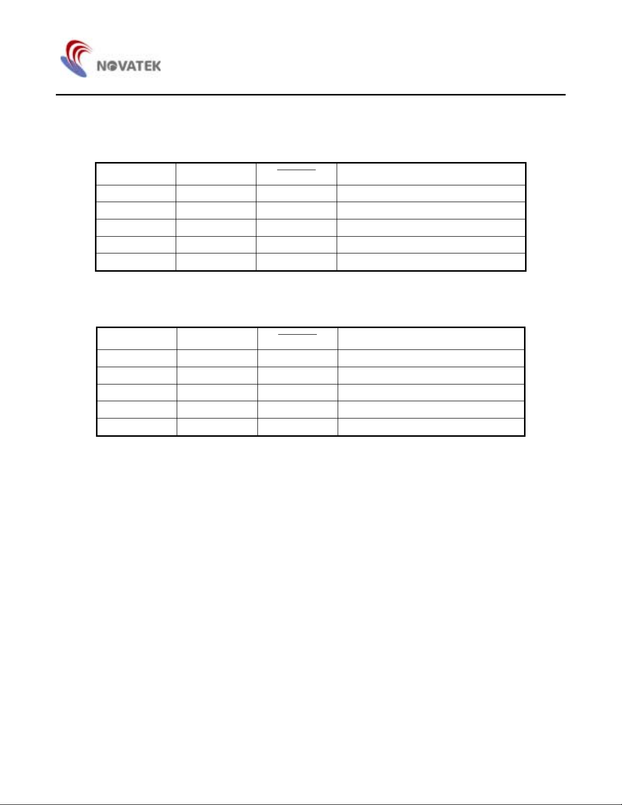
2. LCD Driver Output Voltage Level
The relationship amongst the data bus signal, AC converted signal FR and LCD driver output voltage is as shown in the table
below:
2.1. Segment Mode
FR Latch Data
DISPOFF
Driver Output Voltage Level (Y
1 - Y160
)
L L H V43
L H H V5
H L H V12
H H H V0
X X L V5
Here, V
SS
≤ V
5
< V
43
< V
12 <V0
, H: V
(+2.5 to +5.5V), L: V
DD
(0V), X: Don't care
SS
2.2. Common Mode
FR Latch Data
DISPOFF
Driver Output Voltage Level (Y
1 - Y160
)
L L H V43
L H H V0
H L H V12
H H H V5
X X L V5
Here, V
SS
≤ V
5
43
< V0, H: V
12
(+2.5 to +5.5V), L: V
DD
(0V), X: Don't care
SS
< V
< V
Note: There are two kinds of power supply (logic level voltage, LCD driver voltage) for the LCD driver. Please supply regular
voltage, which assigned by specification for each power pin.
That time "Don't care" should be fixed to "H" or "L", avoiding floating.
11
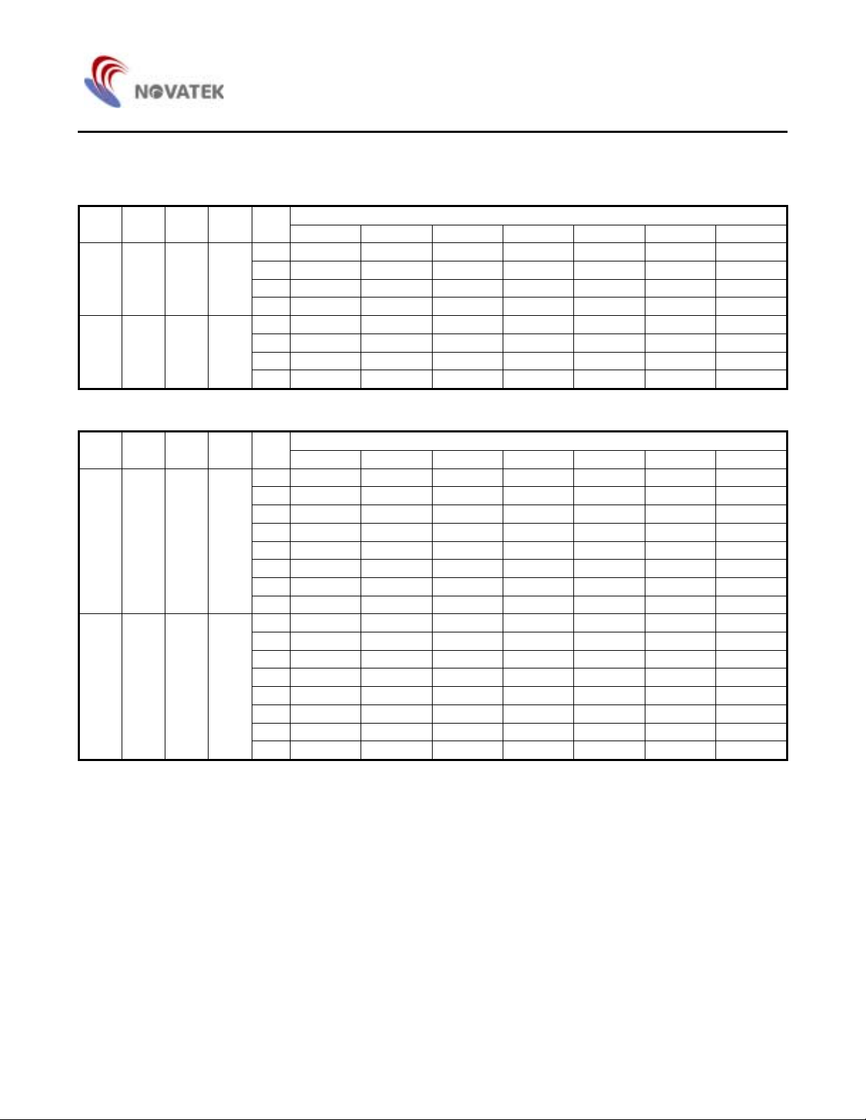
3. Relationship between the Display Data and Driver Output Pins
3.1. Segment Mode:
(a) 4-bit Parallel Mode
MD L/R EIO1 EIO2
Data
Input
40clock 39clock 38clcok ~ 3clock 2clock 1clock
D0 Y1 Y5 Y9
L L Output Input
D1 Y2 Y6 Y10
D2 Y3 Y7 Y11
Y4 Y8 Y12
3
D
D0 Y160 Y156 Y152
L H Input Output
D1 Y159 Y155 Y151
D2 Y158 Y154 Y150
D
Y157 Y153 Y149
3
(b) 8-bit Parallel Mode
MD L/R EIO1 EIO2
Data
Input
20clock 19clock 18clcok ~ 3clock 2clock 1clock
D0 Y1 Y9 Y17 ~ Y137 Y145 Y153
D1 Y2 Y10 Y18 ~ Y138 Y146 Y154
D2 Y3 Y11 Y19 ~ Y139 Y147 Y155
H L Output Input
D3 Y4 Y12 Y20 ~ Y140 Y148 Y156
D4 Y5 Y13 Y21 ~ Y141 Y149 Y157
D5 Y6 Y14 Y22 ~ Y142 Y150 Y158
D6 Y7 Y15 Y23 ~ Y143 Y151 Y159
Y8 Y16 Y24 ~ Y144 Y152 Y160
7
D
D0 Y160 Y152 Y144 ~ Y24 Y16 Y8
D1 Y159 Y151 Y143 ~ Y23 Y15 Y7
D2 Y158 Y150 Y142 ~ Y22 Y14 Y6
H H Input Output
D3 Y157 Y149 Y141 ~ Y21 Y13 Y5
D4 Y156 Y148 Y140 ~ Y20 Y12 Y4
D5 Y155 Y147 Y139 ~ Y19 Y11 Y3
D6 Y154 Y146 Y138 ~ Y18 Y10 Y2
Y153 Y145 Y137 ~ Y17 Y9 Y1
7
D
Number of Clock
~
~
~
~
~
~
~
~
Number of Clock
NT7701
Y149 Y153 Y157
Y150 Y154 Y158
Y151 Y155 Y159
Y152 Y156 Y160
Y12 Y8 Y4
Y11 Y7 Y3
Y10 Y6 Y2
Y9 Y5 Y1
12
 Loading...