NOVATEK NT7502H-TABF1, NT7502H-BDT Datasheet
NT7502
65 X 132 RAM-Map LCD Controller / Driver
Features
! Direct RAM data display using the display RAM. When
RAM data bit is 0, it is not displayed. When RAM data bit
is 1, it is displayed. (At normal display)
! RAM capacity: 65 X 132 = 8580 bits
! Many command functions: Read/Write Display Data.
Display ON/OFF. Normal/Reverse Display. Page
Address Set. Set Display Start Line. Set LCD Bias,
Electronic contrast Controls, V0 voltage regulation
internal resistor ratio set, Read Modify Write, Select
Segment Driver Direction, Power Save
! High-speed 8-bit microprocessor interface allowing direct
connection to both the 8080 and 6800
! Serial interface
! Power supply voltage: 2.4 - 3.5V
! Maximum 12V LCD driving output voltage
! 2X / 3X / 4X on chip DC-DC converter
! Voltage regulator
! Voltage follower
! On-chip oscillator
General Description
The NT7502 is a single-chip LCD driver for dot-matrix liquid
crystal displays which is directly connectable to a
microcomputer bus. It accepts 8-bit serial or parallel display
data directly sent from a microcomputer and stores it in an
on-chip display RAM. It generates a LCD drive signal
independent of the microprocessor clock.
The set of the on-chip display RAM of 65 X 132 bits and a
one-to-one correspondence between LCD panel pixel dots
and on-chip RAM bits permit implementation of displays with
a high degree of freedom.
The NT7502 contains 65 common output circuits and 132
segment output circuits, so that a single chip of NT7502 can
make 65 X 132, 55 X 132, 49 X 132 and 33 X 132 dot
displays with pad option (DUTY1, DUTY0).
No external operation clock is required for RAM read/write
operations. Accordingly, this driver can be operated with a
minimum current consumption and its onboard
low-current-consumption liquid crystal power supply can
implement a high-performance handy display system with
minimum current consumption and the smallest LSI
configuration.
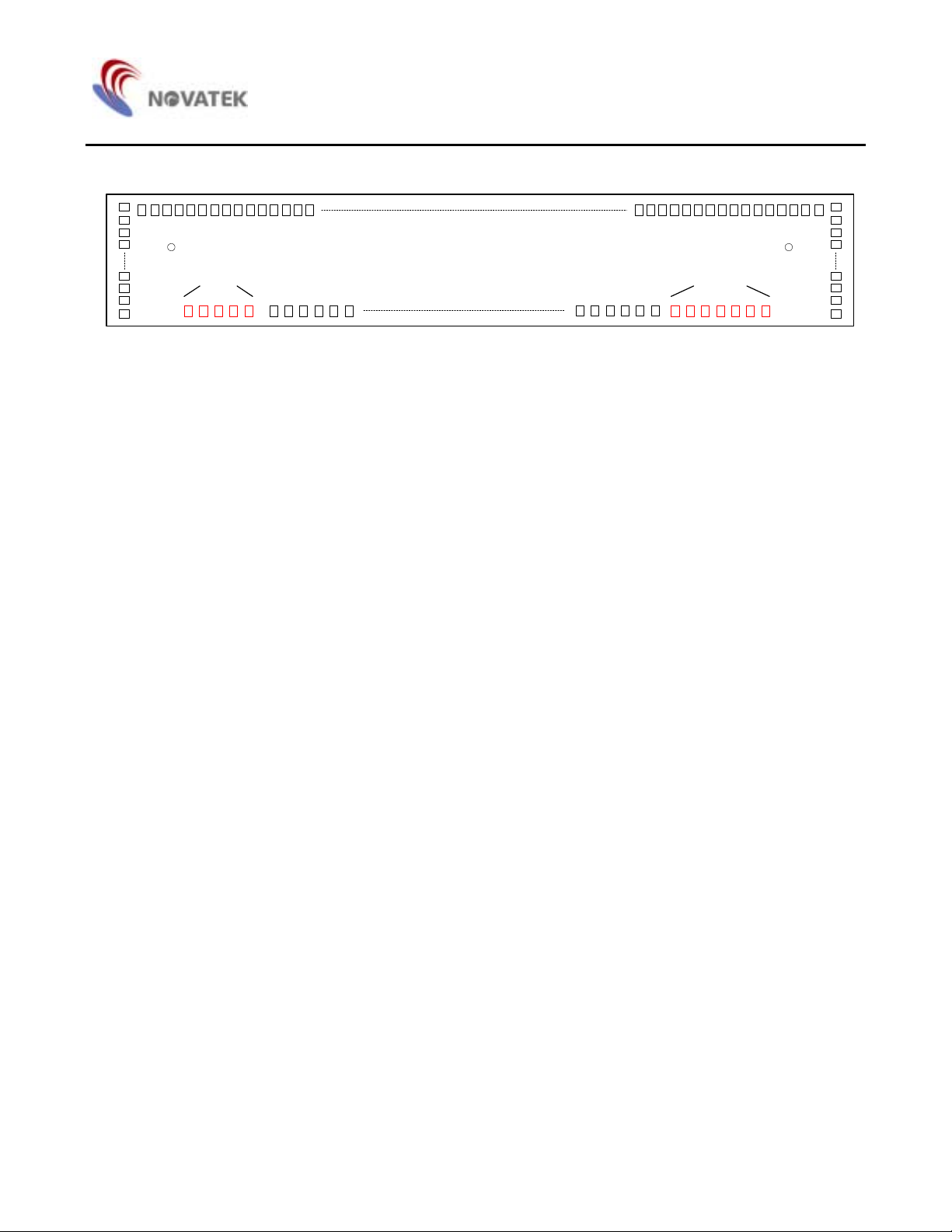
Pin Configuration
SEG130
48COM31
COM30
COM29
495051
COM28
COMS
COM1
COM0
SEG0
7879808182
SEG1
SEG2
83
SEG131
COM32
COM33
211
212
213
214
COM62
COM34
215
COM63
COMS
FRS
FR
243
244
245
246
247
NT7502H-TABF1
(Copper Side View)
40414243444546
47
P/S
HPM
IRS
39
V4
V3NCV0VRM/S
CLS
C86
+CAP2-VEXT
VRSV1V2
CAP1
+
VDD2
VSS
VOUTNCCAP3+CAP1-CAP2
1 V1.0
1011121314151617181920212223242526272829303132333435363738
CS1
CS2
RESA0WRRDD0D1D2D3D4D5D6D7DUTY0DUTY1VDD
NC
123456789
NCNCNCNCFRCLDOF
NT7502
Pad Configuration
281
282
ALK_L ALK_R
118
NT7502
DUMMY DUMMY
298
DUMMY0 DUMMY4 DUMMY5 DUMMY11
1001
117
101
2
NT7502
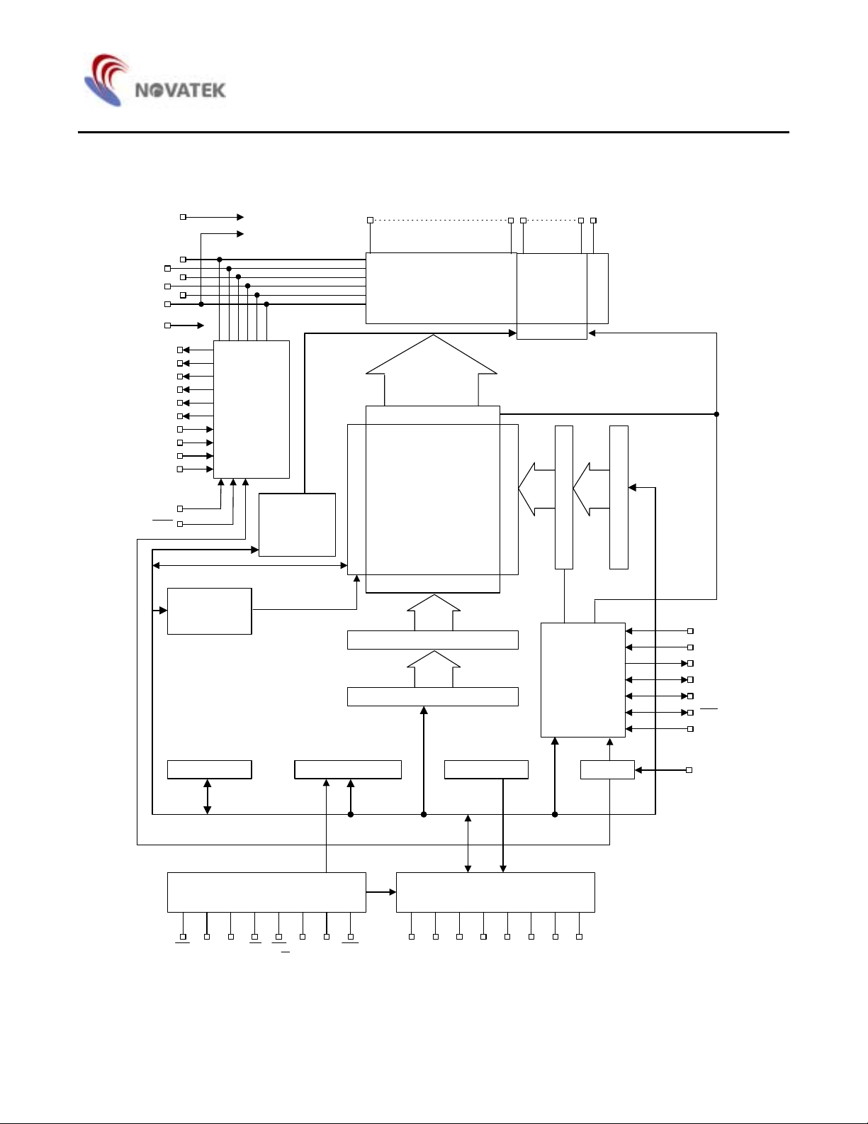
Block Diagram
V1
V3
Vss
TMPS
CAP1+
CAP1-
CAP2+
CAP2-
CAP3+
V
DD
V
0
V2
V4
V
EXT
OUT
V
V
DD2
V
R
V
RS
IRS
HPM
Page address
Power Supply
register
Circuit
Output
status
selector
circuit
SEG0
SEG131
Segment driver
Display data latch
132*65-dot
display data RAM
I/O buffer circuit
Column address decoder
8-bit column address counter
8-bit column address counter
COM0 COM63 COMS
Common
driver
Shift register
Line counter
line address decoder
Display timing
generator
circuit
COM S
Initial display line register
DUTY0
DUTY1
FRS
FR
CL
DOF
M/S
Bus holder Command decoder Bus holder
Oscillator
CLS
Microprocessor interface I/O buffer
CS2 A0
RD
(E)
WR
C86 P/S
)W/R(
RES1CS
D7
(SI)
D5 D4 D3 D2 D1 D0
D6
(SCL)
3
NT7502
V1V2V3V
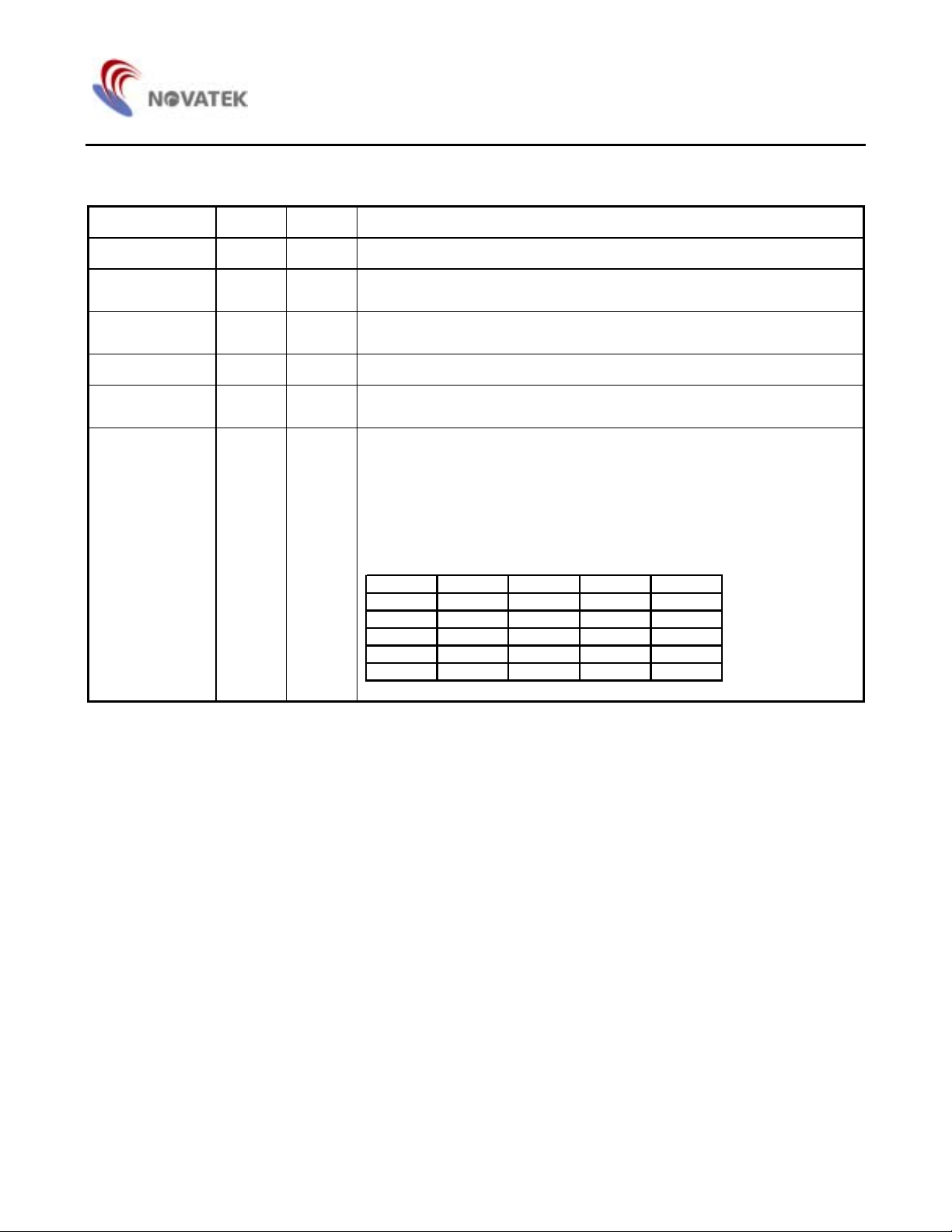
Pad Description
Power Supply
Pad No. Symbol I/O Descriptions
30 - 33 VDD Supply 2.4 - 3.5V power supply input. These pads must be connected each other
10, 16, 26, 53, 71,
77, 81, 91
34 - 36 VDD2 Supply
DD Supply 2.4 - 3.5V power supply output for pad option
V
This is the reference power supply for the step-up voltage circuit for the LCD.
These pads must be connected each other
37 - 40 VSS Supply Ground. These pads must be connected each other
7, 13, 25, 29 , 56,
69 - 70, 74, 79, 83
V
SS Supply Ground output for pad option
LCD driver supply voltages. The voltage determined by LCD cell is
impedance-converted by a resistive driver or an operation amplifier for
application. Voltages should be according to the following relationship:
0 ≥ V1 ≥ V2 ≥ V3 ≥ V4 ≥ VSS
65 - 66
57 - 58
59 - 60
61 - 62
63 - 64
V
V
V2
V3
V4
0
1
Supply
V
When the on-chip operating power circuit is on, the following voltages
are supplied to V
1 to V4 by the on-chip power circuit. Voltage selection is
performed by the Set LCD Bias command.
LCD bias
1/5 bias 4/5V0 3/5V0 2/5V0 1/5V0
1/6 bias 5/6V0 4/6V0 2/6V0 1/6V0
1/7 bias 6/7V0 5/7V0 2/7V0 1/7V0
1/8 bias 7/8V0 6/8V0 2/8V0 1/8V0
1/9 bias 8/9V0 7/9V0 2/9V0 1/9V0
4
4

NT7502
LCD Driver Supplies
Pad No. Symbol I/O Descriptions
45 - 46 CAP1- O Capacitor 1- pad for internal DC/DC voltage converter
47 - 48 CAP1+ O Capacitor 1+ pad for internal DC/DC voltage converter
51 - 52 CAP2- O Capacitor 2- pad for internal DC/DC voltage converter
49 - 50 CAP2+ O Capacitor 2+ pad for internal DC/DC voltage converter
43 - 44 CAP3+ O Capacitor 3+ pad for internal DC/DC voltage converter
41 - 42 VOUT O DC/DC voltage converter output
67 - 68 VR I
54 VEXT I
82 TMPS I
55 VRS I
Voltage adjustment pad. Applies voltage between V
0 and VSS using a
resistive divider
This is the external input reference voltage (VREF) for the internal
voltage regulator. It is valid only when external V
EXT must be ≥ 2.4V and ≤ VDD2
V
When using internal V
REF, this pad must be NC
REF is used.
Selects temperature coefficient of the reference voltage
TMPS = 0: -0.05% / °C
TMPS = 1: -0.2 % / °C
Select the internal voltage regulator or external voltage regulator,
VRS = 0: using the external VREF
VRS = 1: using the internal VREF
5
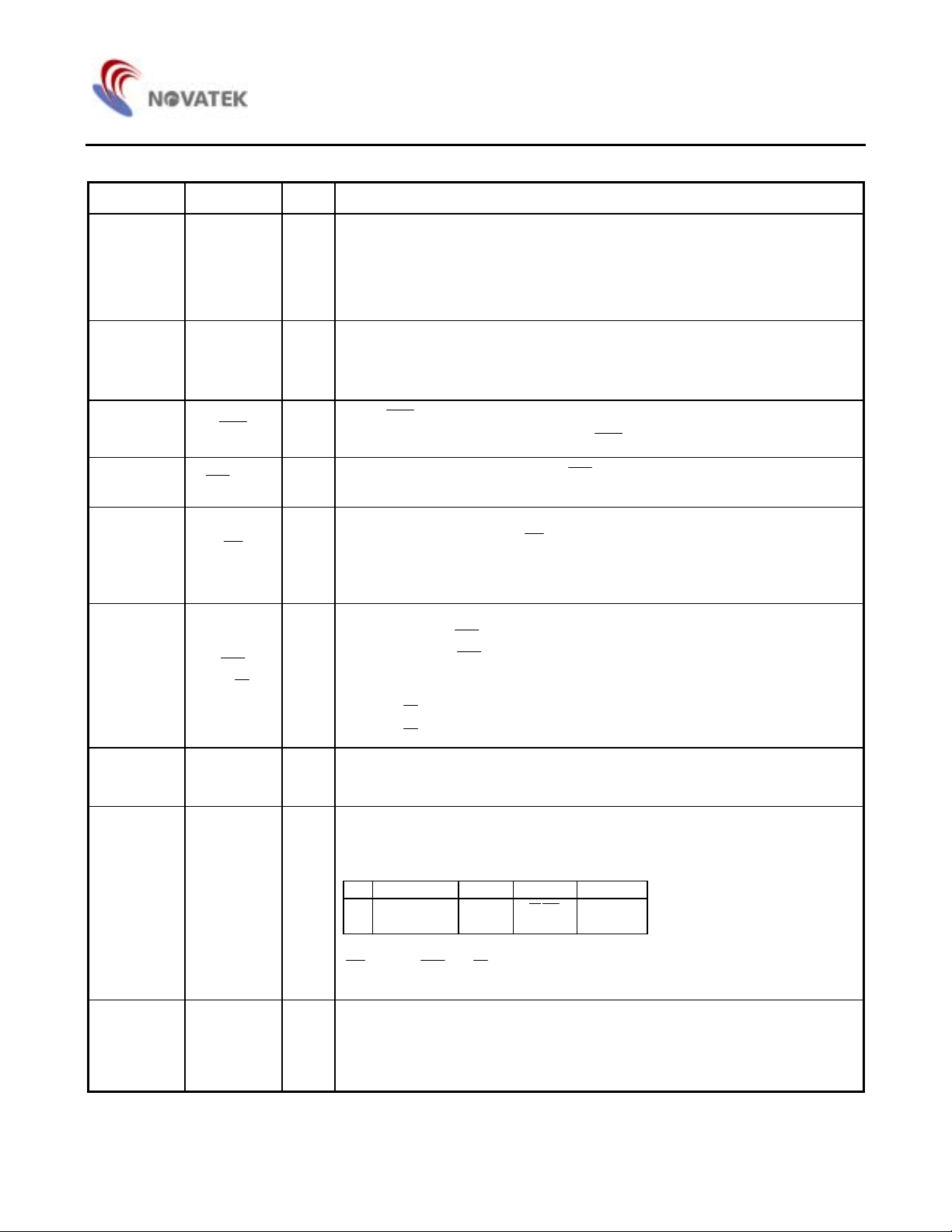
NT7502
System Bus Connection Pads
Pad No. Symbol I/O Descriptions
This is an 8-bit bi-directional data bus that connects to an 8-bit or 16-bit
standard MPU data bus.
When the serial interface is selected (P/S = “L”), then D7 serves as the serial
I/O
data input terminal (SI) and D6 serves as the serial clock input terminal (SCL)
At this time, D0 to D5 are set to high impedance.
17 - 24
D0 - D7
(SI)
(SCL)
When the chip select is inactive, D0 to D7 are set to high impedance.
This is connected to the least significant bit of the normal MPU address bus,
12 A0 I
and it determines whether the data bits are data or a command
A0 = “H” indicating that D0 to D7 are display data, and
A0 = “L” indicating that D0 to D7 are control data.
When
11
RES
I
RES is set to “L”, the settings are initialized.
The reset operation is performed by the
RES signal level.
This is the chip select signal. When
8, 9
1CS CS2
I
select becomes active, and data/command I/O is enabled.
When connected to an 8080 MPU, it is active LOW.
15
RD
(E)
This pad is connected to the
I
data bus is in an output status when this signal is “L”.
When connected to a 6800 Series MPU, this is active HIGH.
This is used as an enable clock input of the 6800 series MPU.
When connected to an 8080 MPU, this is active LOW. This terminal connects
to the 8080 MPU
14
(
WR
W/R )
rising edge of the
I
When connected to a 6800 Series MPU, this is the read/write control signal
input terminal.
When
When
This is the MPU interface switch terminal
75 C86 I
C86 = “H”: 6800 Series MPU interface
C86 = “L”: 8080 MPU interface
This is the parallel data input/serial data input switch terminal
P/S = “H”: Parallel data input
P/S = “L”: Serial data input
The following applies depending on the P/S status:
76 P/S I
P/S Data/Command Data Read/Write Serial Clock
"H" A0 D0 to D7
"L" A0 SI (D7) Write only SCL (D6)
When P/S = “L”, D0 to D5 are HZ. D0 to D5 may be “H”, “L” or Open.
RD(E) and WR ( WR/ ) are fixed to either “H” or “L”. With serial data input,
RAM display data reading is not supported.
1CS = “L” and CS2 = “H”, then the chip
RD signal of the 8080MPU, and the NT7502
WR signal. The signals on the data bus are latched at the
WR signal.
WR/ = “H”: Read
WR/ = “L”: Write
RDWR
Terminal is used to select whether enable or disable the display clock internal
oscillator circuit.
73 CLS I
CLS = “H”: Internal oscillator circuit is enabled
CLS = “L”: Internal oscillator circuit is disabled (requires external input).
When CLS = “L”, input the display clock through the CL pad.
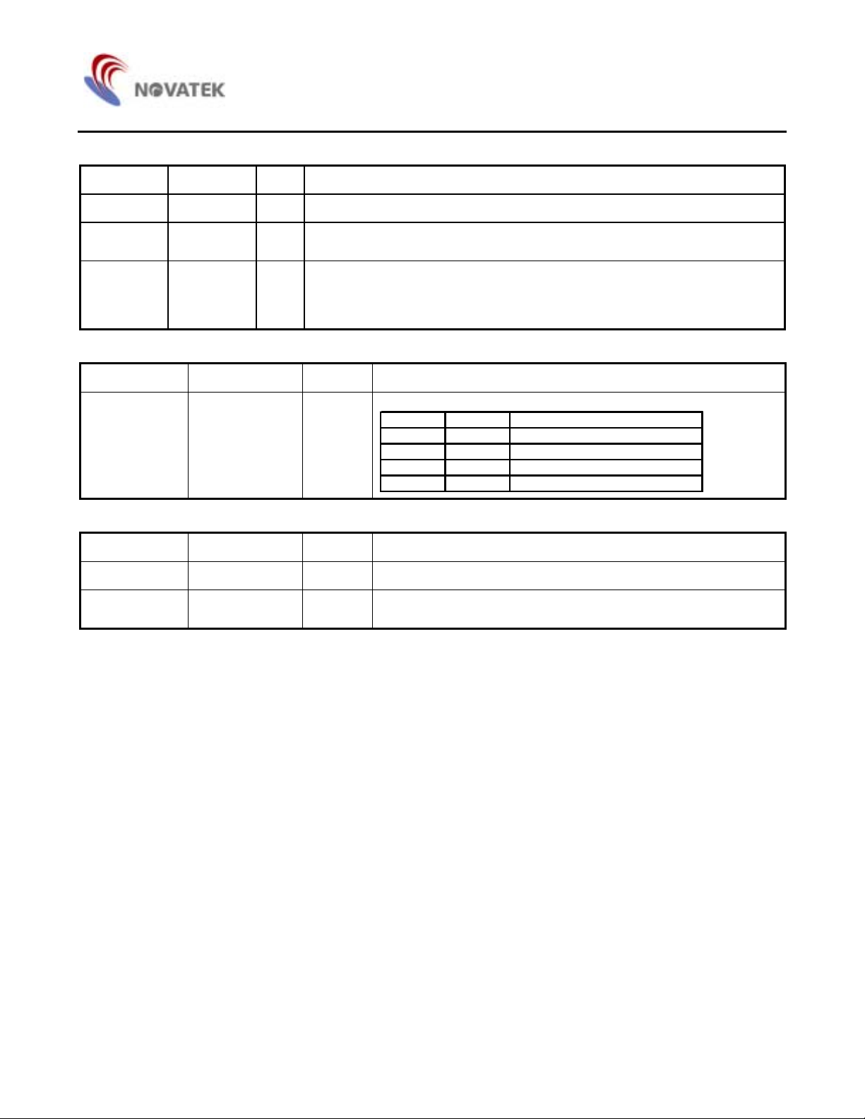
6

DOF
This terminal selects the master/slave operation for the NT7502 chips.
Master operation outputs the timing signals that are required for the LCD display,
while slave operation inputs the timing signals required for the liquid crystal display,
synchronizing the liquid crystal display system.
This is the display clock input terminal.
When the NT7502 chips are used in master/slave mode, the various CL
terminals must be connected.
This is the liquid crystal alternating current signal I/O terminal
M/S = “H”: Output.
M/S = “L”: Input.
When the NT7502 chip is used in master/slave mode, the various FR terminals
must be connected.
This is the liquid crystal display blanking control terminal.
M/S = “H”: Output.
M/S = “L”: Input.
I/O
When the NT7502 chip is used in master/slave mode, the various
must be connected.
This is the output terminal for the static drive.
This terminal is only enabled when the static indicator display is ON in
master operation mode, and is used in conjunction with the FR terminal.
DOF terminals
NT7502
System Bus Connection Pads (continue)
Pad No. Symbol I/O Description
72 M/S I
4 CL I/O
3 FR I/O
5
2 FRS O
80 IRS I
78
HPM
This terminal selects the resistors for the V0 voltage level adjustment
IRS = “H”, Use the internal resistors.
IRS = “L”, Do not use the internal resistors.
The V0 voltage level is regulated by an external resistive voltage divider
attached to the VR terminal.
This pad is enabled only when the master operation mode is selected.
It is fixed to either “H” or “L” when the slave operation mode is selected.
This is the power control terminal for the power supply circuit for liquid
crystal drive.
HPM = “H”, Normal mode
I
HPM = “L”, High power mode
This pad is enabled only when the master operation mode is selected.
It is fixed to either “H” or “L” when the slave operation mode is selected.
7
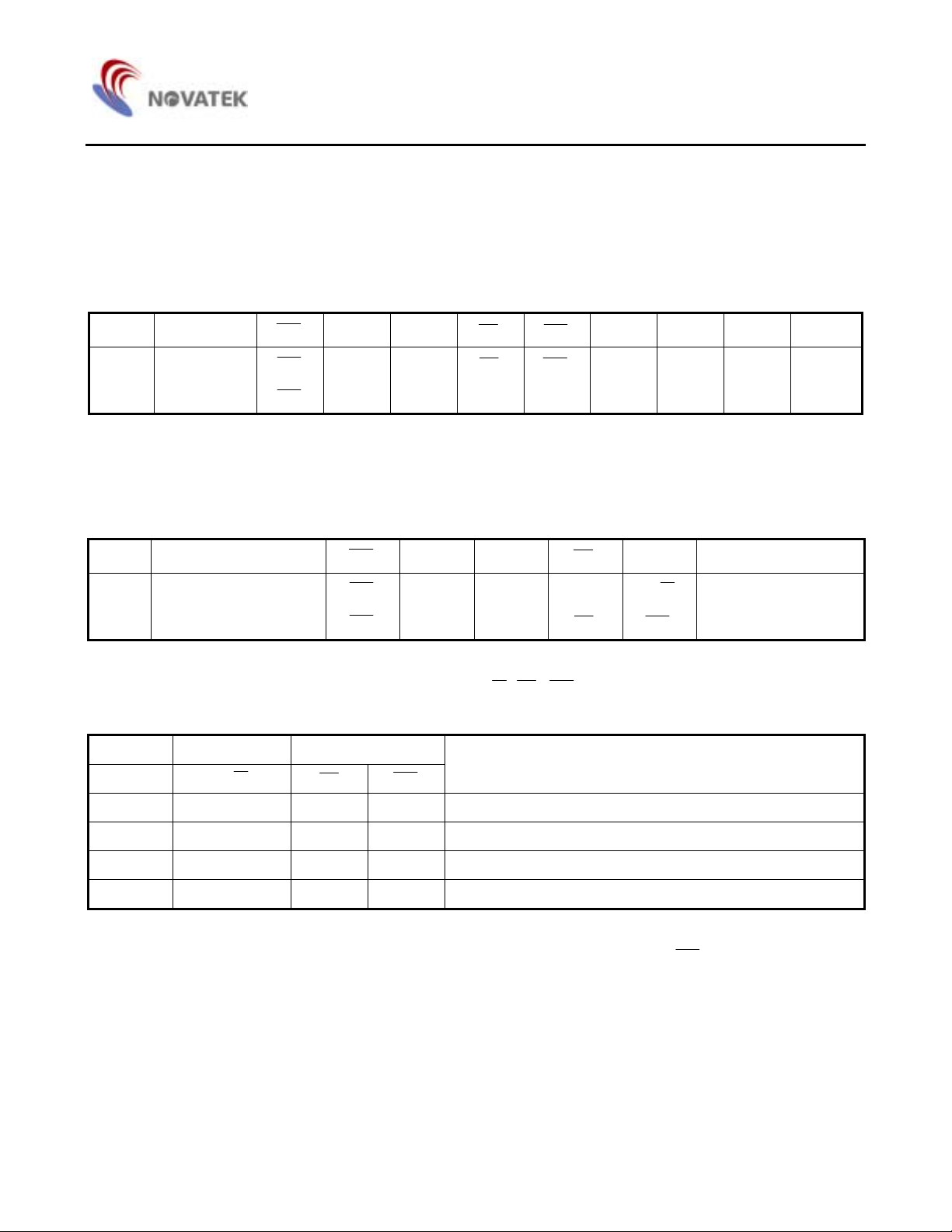
NT7502
y
Liquid Crystal Drive Pads
Pad No. Symbol I/O Description
134 - 265 SEG0 - 131 O Segment signal output for LCD display
101 - 132
266 - 297
133, 298 COMS O
Configuration Pads
Pad No. Symbol I/O Description
27, 28 DUTY0, DUTY1 I
Test Pads
Pad No. Symbol I/O Description
90 TEST3 I Test pads, and must be connected to VDD
1, 6, 84 - 89
92 - 100
COM31 - 0
COM32 - 63
NC NC pads, no connection for user
Common signal output for LCD display
O
When in master/slave mode, the same signal is output by both master and slave
These are the COM output terminals for the indicator. Both terminals output the
same signal
No connect these terminals if they are not used
When in master/slave mode, the same signal is output by both master and slave
Select the LCD driver duty
DUTY1 DUTY0 LCD driver dut
0 0 1/33
0 1 1/49
1 0 1/55
1 1 1/65
8
NT7502
Functional Description
Microprocessor Interface
Interface type selection
The NT7502 can transfer data via 8-bit bi-directional data bus (D7 to D0) or via serial data input (SI). When high or lo w is
selected for the parity of P/S pad, either 8-bit parallel data input or serial data input can be selected as shown in Table 1. When
serial data input is selected, the RAM data cannot be read out.
Table. 1
P/S Type
H Parallel Input
L Serial Input
Parallel Input
When the NT7502 selects parallel input (P/S = high), the 8080 series microprocess or or 6800 series microprocessor can be
selected by causing the c86 pad to go high or low as shown in Table 2.
C86 Type
H 6800 microprocessor bus
L 8080 microprocessor bus
Data Bus Signals
The NT7502 identifies the data bus signal according to A0, E,
Common 6800 processor 8080 processor
A0
1 1 0 1 Reads display data
W/R )
(
1CS
1CS
1CS
CS2 A0
CS2 A0
CS2 A0 - - - SI SCL (HZ)
1CS
1CS
1CS
RD WR
CS2 A0
CS2 A0 E
CS2 A0
RD WR
RD WR
Table. 2
WR/ (RD , WR ) signals.
Table. 3
C86 D7 D6 D0 to D5
C86 D7 D6 D0 to D5
“-” Must always be high or low
RD
RD WR
WR D0 to D7
WR/
Function
D0 to D7
D0 to D7
1 0 1 0 Writes display data
0 1 0 1 Reads status
0 0 1 0 Writes control data in internal register. (Command)
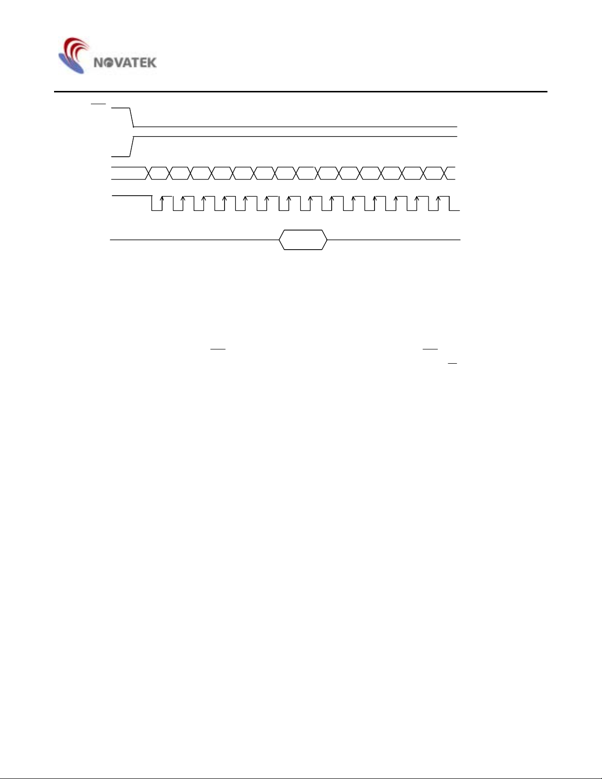
Serial Interface (P/S is low)
When the serial interface has been selected (P/S = “L”), then when the chip is in active state (
serial data input (SI) and the serial clock input (SCL) can be received. The serial data is read from the serial data input pin in the
rising edge of the serial clocks D7, D6 through D0, in this order. This data is converted to 8 bits of parallel data in the rising edge
of eighth serial clock for processing.
The A0 input is used to determine whether or the serial data input is display data, and when A0 = “L” then the data is command
data. The A0 input is read and used for detection every 8th rising edge of the serial clock after the chip becomes active.
Figure 1 is the serial interface signal chart.
9
1CS = “L” and CS2 = “H”), the
NT7502
1CS
CS2
SI
SCL
A0
D7 D6 D5 D4 D3 D2 D1 D0 D7 D6 D5 D4 D3 D2
123456 789101112 13 14
Figure. 1
# When the chip is not active, the shift registers and the counter are reset to their initial states.
# Reading is not possible while in serial interface mode.
# Caution is required on the SCL signal when it comes to line-end reflections and external noise. We recommend the
operation be rechecked on the actual equipment.
Chip Select Inputs
The NT7502 has two chip select pads.
When these pads are set to any other combination, D0 to D7 are high impedance and A0, E and
1CS and CS2 can interface to a microprocessor when 1CS is low and CS2 is high.
WR/ inputs are disabled.
When serial input interface is selected. the shift register and counter are reset.
Access to Display Data RAM and Internal Registers
The NT7502 can perform a series of pipeline processing between LSI’s using the bus holder of the internal data bus in order to
match the operating frequency of display RAM and internal registers with the microprocessor. For example, the microprocessor
reads data from display RAM in the first read (dummy) cycle, stores it in the bus holder, and outputs it onto system bus in the
next data read cycle.
Also, the microprocessor temporarily stores display data in the bus holder, and stores it in display RAM until the next data write
cycle starts.
When viewed from the microprocessor, the NT7502 access speed greatly depends on the cycle time rather than access time to
the display RAM (t
ACC). This view shows the data transfer speed to / from the microprocessor can increase. If the cycle time is
inappropriate, the microprocessor can insert the NOP instruction that is equivalent to the wait cycle setup. However, there is a
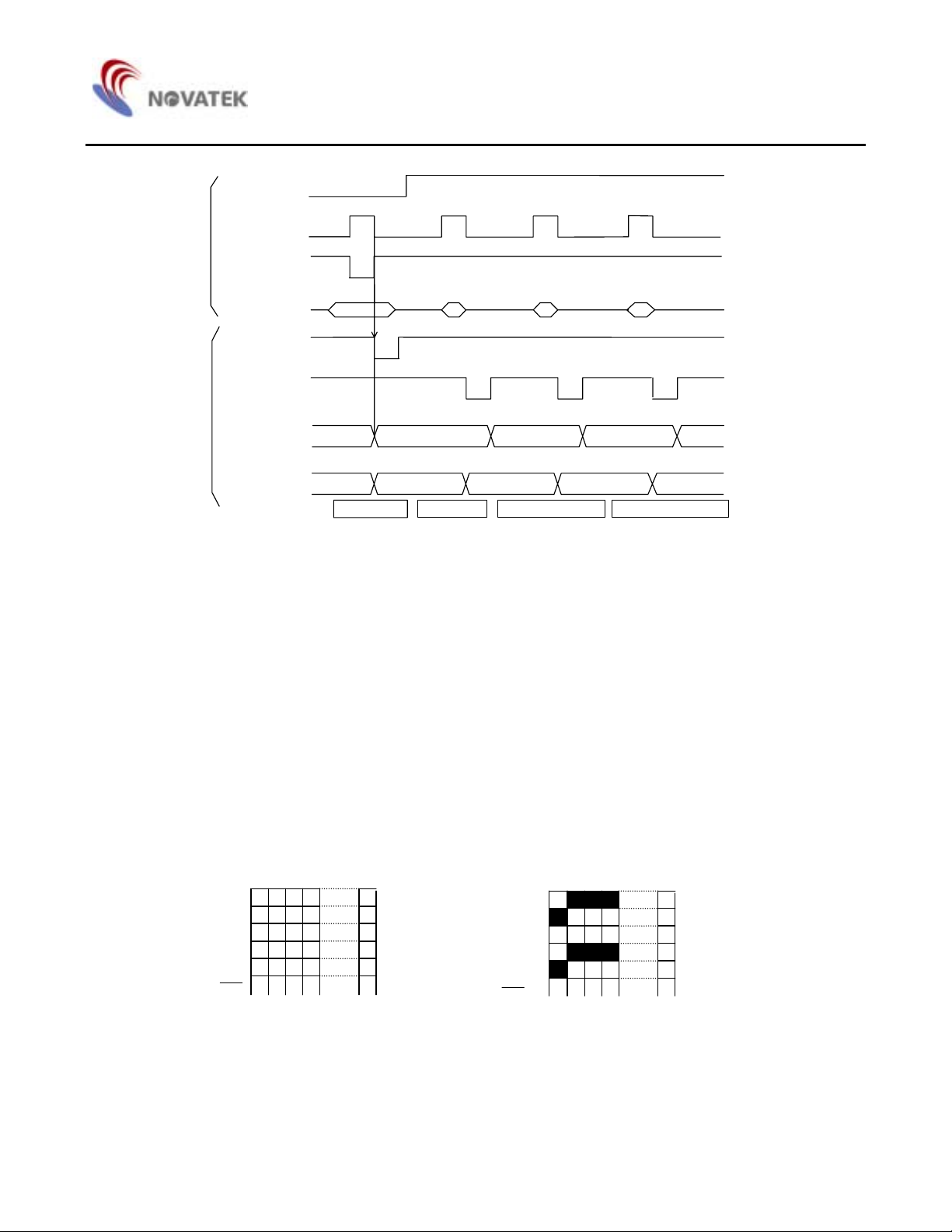
restriction in the display RAM read sequence. When an address is set, the specified address data is NOT output at the
immediately following read instruction. The address data is output during the second data read. A single dummy read must be
inserted after address setup and after the write cycle (refer to Figure2).
10
NT7502
A0
MPU
Internal
timing
E
R/W
DATA
Address preset
Read signal
Column address
BUS holder
N
Preset
Set address n Dummy read Data Read address n Data Read address n+1
N
N N+1 N+2
N n n+1
n n+1
Incremented
n+2
Figure. 2
Busy Flag
When the busy flag is “1”, it indicates that the NT7502 chip is running internal processes, and at this tim e no command asi de
from a status read will be received. The busy flag is outputted to D7 pad with the read instruction. If the cycle time (t
maintained,
it is not necessary to check for this flag before each command. This makes vast improvements in MPU processing
CYC) is
capabilities possible.
Display Data RAM
Display Data RAM
The display data RAM is RAM that stores the dot data for the display. It has a 65 (8 page * 8 bit+1)*132 bit structure. It is
possible to access the desired bit by specifying the page address and the column ad dress. Because, as is sho wn in Figure3,
the D7 to D0 display data from the MPU corresponds to the liquid crystal display common direction, there are few constraints at
the time of display common direction, and there are few constraints at the time of displa y data transfer when multiple NT7502
chips are used, thus display structures with a high degree of freedom can be created easily .
Moreover, reading from and writing to the display RAM from the MPU side is performed through the I/O buffer, which is an
independent operation from signal reading for the liquid crystal driver. Consequently, even if the display data RAM is accessed
asynchronously during liquid crystal display, it will not cause adverse effects on the displ ay (such as flickering).
D0
D1
D2
D3
D4
111
0
000
1
0000
111
0
000
1
0
0
0
0
0
COM0
COM1
COM2
COM3
COM4
Display data RAM Display on LCD
Figure. 3
11

NT7502
The Page Address Circuit
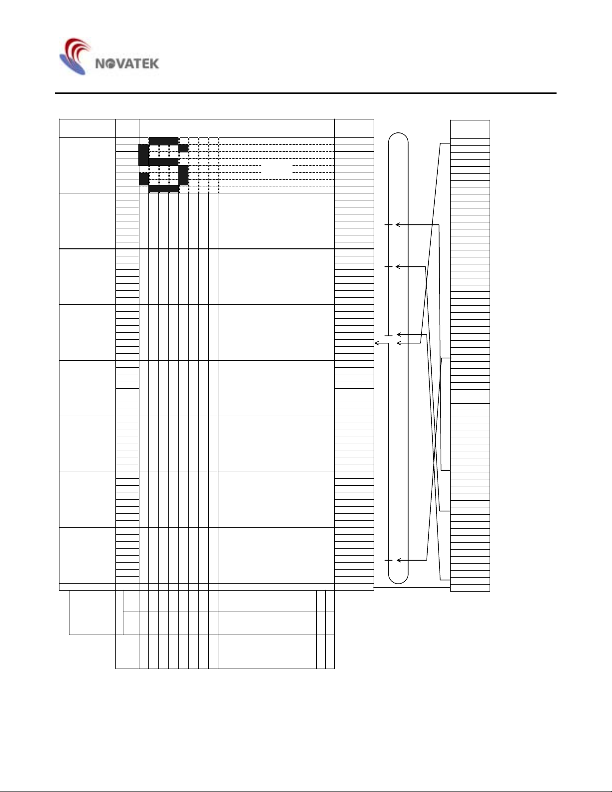
As shown in Figure 4, page address of the display data RAM is specified through the Page Address Set Command. The page
address must be specified again when changing pages to perform access.
Page address8 (D3, D2, D1, D0 = 1, 0, 0, 0,) is the page for the RAM region used; only display data D0 is used.
The Column Address
As shown in Figure 4, the display data RAM column address is specified by the Column Address Set command. The specified
column address is incremented (+1) with each display data read / write command. This allows the MPU display data to be
accessed continuously. Moreover, the incrimination of column addresses stops with 83H, because the column address is
independent of the page address. Thus, when moving, for exam ple, from page0 column 83H to page 1 column 00H, it is
necessary to respecify both the page address and the column address.
Furthermore, as is shown in Table 4, the ADC command (segment driver direction select command) can be used to reverse the
relationship between the display data RAM column address and the segment output. Because of this, the constraints on the IC
layout can be minimized when the LCD module is assembled.
Table. 4
SEG Output SEG0 SEG131
ADC “0” 0 (H)$ Column Address $83 (H)
(ADC) “1” 83 (H)% Column Address %0 (H)
The Line Address Circuit
The line address circuit, as shown in Table 4, specifies the line address relating to the COM output when the conten ts of the
display data RAM are displayed. Using the display start line address set command, what is normally the top line of the display
can be specified. This is the COM0 output when the common output mode is normal, and the COM63 output for NT7502, when
the common output mode is reversed. The display area is a 65-line area for the NT7502 from the display start line address.
If the line addresses are changed dynamically using the display start line address set command, screen scrolling, page
swapping, etc. can be performed.
12
NT7502
Relationship between display data RAM and address. (if initial display line is 1DH)
Page Address Data
D0 00
D1 01
D3, D2,
D1, D0
0, 0, 0, 0
0, 0, 0, 1
0, 0, 1, 0
0, 0, 1, 1
0, 1, 0, 0
0, 1, 0, 1
0, 1, 1, 0
0, 1, 1, 1
1, 0, 0, 0 D0 Page8
Column
D2 02
D3 03
D4 04
D5 05
D6 06
D7 07
D0 08
D1 09
D2 0A
D3 0B
D4 0C
D5 0D
D6 0E
D7
D0 10
D1 11
D2 12
D3 13
D4 14
D5 15
D6 16
D7
D0 18
D1 19
D2 1A
D3 1B
D4 1C
D5 1D
D6 1E
D7
D0 20
D1 21
D2 22
D3 23
D4 24
D5 25
D6 26
D7
D0 28
D1 29
D2 2A
D3 2B
D4 2C
D5 2D
D6 2E
D7
D0 30
D1 31
D2 32
D3 33
D4 34
D5 35
D6 36
D7
D0 38
D1 39
D2 3A
D3 3B
D4 3C
D5 3D
D6 3E
D7
000102
“0”
D0=
ADC
address
D0=
”1”
838281
Page0
Page1
Page2
Page3
Page4
Page5
Page6
Page7
818283
020100
Line
Address
0F
17
1F
27
2F
37
3F
Start
COM
output
COM0
COM1
COM2
COM3
COM4
COM5
COM6
COM7
COM8
COM9
COM10
COM11
COM12
COM13
COM14
COM15
COM16
COM17
COM18
COM19
COM20
COM21
COM22
COM23
COM24
COM25
COM26
COM27
COM28
COM29
COM30
COM31
COM32
COM33
COM34
COM35
COM36
COM37
COM38
COM39
COM40
COM41
COM42
COM43
COM44
COM45
COM46
COM47
COM48
COM49
COM50
COM51
COM52
COM53
COM54
COM55
COM56
COM57
COM58
COM59
COM60
COM61
COM62
COM63
COMS
LCD
OUT
SEG0
SEG1
SEG2
SEG129
SEG130
SEG131
Figure. 4
13
NT7502
The Display Data Latch Circuit
The display data latch circuit is a latch that temporarily stores the display data output to the liquid crystal driver circuit from the
display data RAM.
Because the display normal/reverse status, display ON/OFF status, and display all points ON/OFF commands control only the
data within the latch, they do not change the data within the display data RAM itself.
The Oscillator Circuit
This is a CR-type oscillator that produces the display clock. The oscillator circuit is only enabled when M/S = “H” and CLS = “H”.
When CLS = “L” the oscillation stops, and the display clock is input through the CL terminal.
Display Timing Generator Circuit
The display timing generator circuit generates the timing signal to the line address circuit and the display data latch circuit using
the display clock. The display data is latched into the display data latch circuit synchronized with the display clock, and is output
to the data driver output terminal. Reading to the display data liquid crystal driver circuits is completely independent of access to
the display data RAM by the MPU. Consequently, even if the display data RAM is accessed as ynchronously during liquid
crystal display, there is absolutely no adverse effect (such as flickering) on the display.
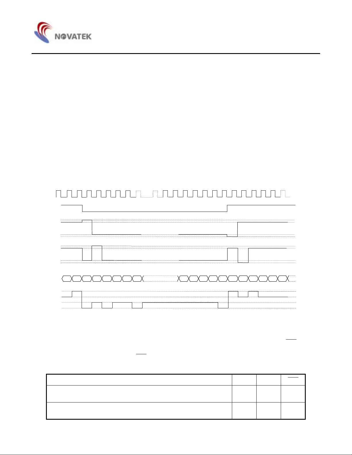
Moreover, the display timing generator circuit generates the common timing and the liquid crystal alternating current signal (FR)
from the display clock. It generates a drive waveform using a 2 frame alternating current drive method, as is shown in Figure 5,
for the liquid crystal drive circuit.
23451 6
CL
FR
61 62 63 64 65
23451
66564
60
V
0
V
V4
V
V
V
V4
V
V
V
V3
V
1
SS
0
1
SS
0
2
SS
COM0
COM1
RAM
data
SEGn
Figure. 5
When multiple NT7502 chips are used, the slave chips must be supplied with the display timing signals (FR, CL, DOF ) from the
master chip[s].
Table 5 shows the status of the FR, CL, and
DOF signals.
Table. 5
Operating Mode FR CL
Master (M/S = “H”) The internal oscillator circuit is enabled (CLS = “H”)
The internal oscillator circuit is disabled (CLS = “L”)
Slave (M/S = “L”) The internal oscillator circuit is disabled (CLS = “H”)
The internal oscillator circuit is disabled (CLS = “L”)
Output
Output
Input
Input
Output
Input
Input
Input
DOF
Output
Output
Input
Input
14
NT7502
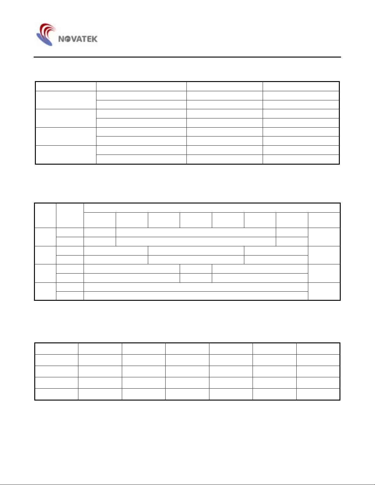
Table 6 shows the relationship between oscillation frequency and frame frequency
Table. 6
Duty Item f
1/65
1/55
1/49
1/33
On-chip oscillator is used fOSC/6 fCL/(2 X 65)
On-chip oscillator is not used External input f
On-chip oscillator is used fOSC/8 fCL/(2 X 55)
On-chip oscillator is not used External input f
On-chip oscillator is used fOSC/8 fCL/(2 X 49)
On-chip oscillator is not used External input f
On-chip oscillator is used fOSC/12 fCL/(2 X 33)
On-chip oscillator is not used External input f
CL fFR
CL fCL/(2 X 65)
CL fCL/(2 X 55)
CL fCL/(2 X 49)
CL fCL/(2 X 33)
Common Output Control Circuit
This circuit controls the relationship between the number of common output and specified duty ratio. Common output mode
select instruction specifies the scanning direction of the common output pads.
Table. 7
Common output pads
Duty Status
1/33
1/49
1/55
1/65
Normal COM[0-15] NC COM[16-31]
Reverse COM[31-16] NC COM[15-0]
Normal COM[0-23] NC COM[24-47]
Reverse COM[47-24] NC COM[23-0]
Normal COM[0-26] NC COM[27-53]
Reverse COM[53-27] NC COM[26-0]
Normal COM[0-63]
Reverse
COM
[0-15]
COM
[16-23]
COM
[24-26]
COM
[27-36]
COM[63-0]
COM
[37-39]
COM
[40-47]
COM
[48-63]
COMS
COMS
COMS
COMS
COMS
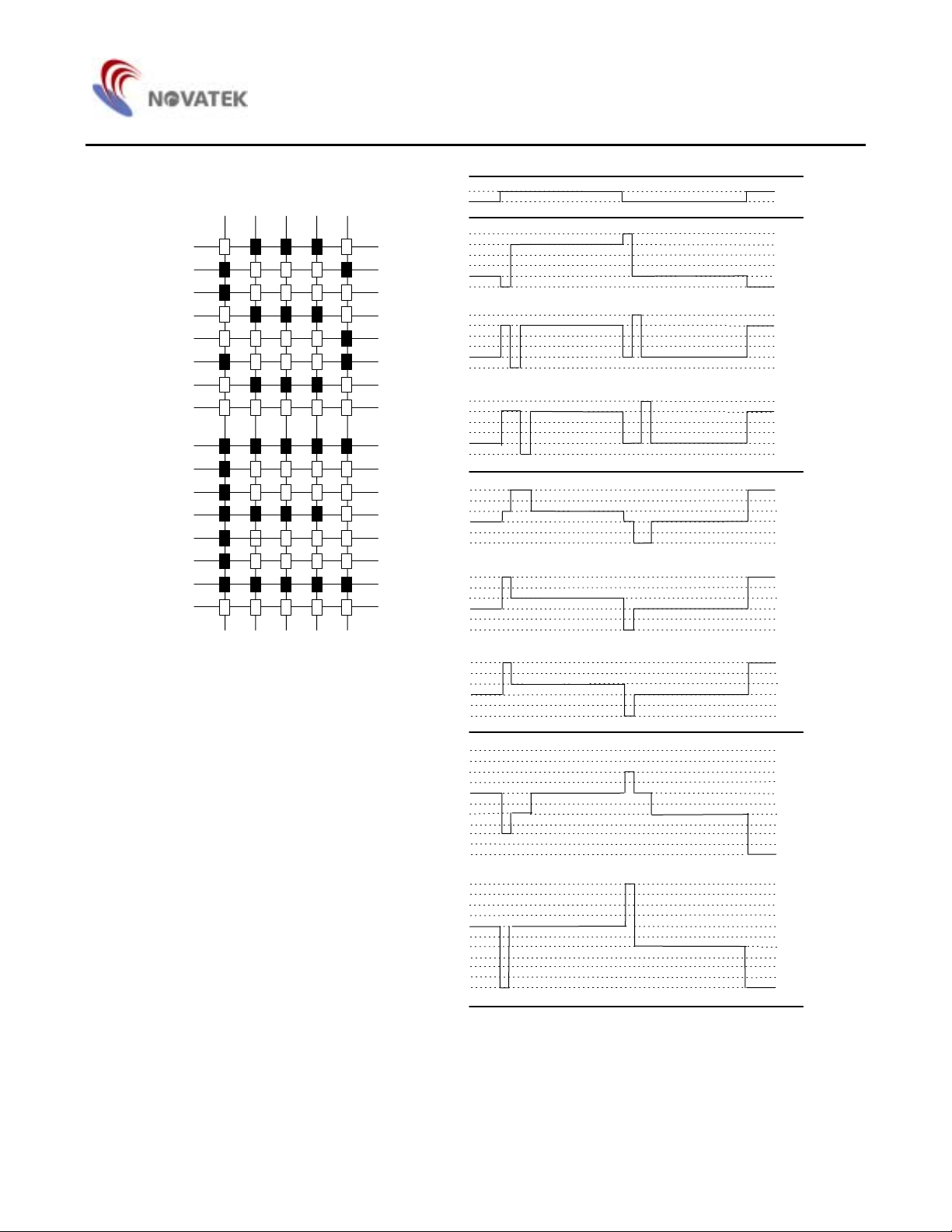
This is a 197-channel multiplexes that generate voltage levels for driving the liquid crystal. The combination of the display data,
the COM scan signal, and the FR signal produces the liquid crystal drive voltage output.
Figure 6 shows example of the SEG and COM output wave form.
Configuration Setting
The NT7502 has two optional configurations, configured b y DUTY0, DUTY1
DUTY1, DUTY0 Common Segment V1 V2 V3 V4
1, 1 65 132 8/9V0, 6/7V0 7/9V0, 5/7V0 2/9V0, 2/7 V0 1/9V0, 1/7V0
1, 0 55 132 7/8V0, 5/6V0 6/8V0, 4/6V0 2/8V0, 2/6 V0 1/8V0, 1/6V0
0, 1 49 132 7/8V0, 5/6V0 6/8V0, 4/6V0 2/8V0, 2/6 V0 1/8V0, 1/6V0
0, 0 33 132 5/6V0, 4/5V0 4/6V0, 3/5V0 2/6 V0, 2/5V0 1/6V0, 1/5V0
15
NT7502
COM0
COM1
COM2
COM3
COM4
COM5
V
FR
COM0
COM1
DD
V
SS
V
0
V
1
V
2
V
3
V
4
V
SS
V
0
V
1
V
2
V
3
V
4
V
SS
COM6
V
COM7
COM8
COM2
0
V
1
V
2
V
3
V
4
V
SS
COM9
V
COM10
COM11
COM12
SEG0
0
V
1
V
2
V
3
V
4
V
SS
COM13
V
COM14
COM15
SEG1
0
V
1
V
2
V
3
V
4
V
SS
SEG2
COM0 - SEG0
COM0 - SEG1
Figure. 6
V
0
V
1
V
2
V
3
V
4
V
SS
V
0
V
1
V
2
V
3
V
4
V
SS
-V
4
-V
3
-V
2
-V
1
-V
0
V
0
V
1
V
2
V
3
V
4
V
SS
-V
4
-V
3
-V
2
-V
1
-V
0
16
NT7502
The Power Supply Circuit
The power supply circuits are low-power consumption power supply circuits that generate the voltage le vels required for the
liquid crystal drivers. They comprise Booster circuits, voltage regulator circuits, and voltage follower circuits. They are only
enabled in master operation.
The power supply circuits can turn the Booster circuits, the voltage regulator circuits, and the vo ltage follower circuits ON or
OFF independently through the use of the Power Control Set command. Consequently, it is possible to make an external power
supply and the internal power supply function somewhat in parallel. Table 7 shows the Power Control Set Command 3-bit data
control function, and Table 8 shows reference combinations.
Table. 8 The Control Details of Each Bit of the Power Control Set Command
Item
Status
“1” “0”
D2 Booster circuit control bit ON OFF
D1 Voltage regulator circuit (V regulator circuit) control bit ON OFF
D0 Voltage follower circuit (V/F circuit) control bit ON OFF
Table. 9
Step-up
voltage
system
terminal
Use Settings D2 D1 D0
1. Only the internal power supply
is used
2. Only the V regulator circuit and
the V/F circuit are used
Step-up
circuit
Voltage
regulator
circuit
V/F circuit
External
voltage input
1 1 1 O O O V
0 1 1 X O O V
OUT, VDD2 Open
DD2 Used
3. Only the V/F circuit is used 0 0 1 X X O V0, VDD2 Open
4. Only the external power supply
is used
0 0 0 X X X V
0 to V4 Open
*The “step-up system terminals” refer CAP1+, CAP1-, CAP2+, CAP2-and CAP3+.
*While other combinations, not shown above, are also possible, these combinations are not recommended because they have
no practical use.
The Step-up Voltage Circuits
Using the step-up voltage circuits within the NT7502 chips it is possible to product 4X, 3X, 2X step-ups of the V
DD2-VSS voltage
levels
17
 Loading...