NOVATEK NT7501H-BDT Datasheet

33 X 100 RAM-Map LCD Controller/Driver
Features
Direct RAM data display using the display RAM. When
!
RAM data bit is 0, it is not displayed. When RAM data bit
is 1, it is displayed. (In normal display mode)
RAM capacity: 65 X 132 = 8580 bits
!
Many command functions: Read/Write Display Data,
!
Display ON/OFF, Normal/Reverse Display, Page
Address Set, Set Display Start Line, Set LCD Bias,
Electronic contrast Controls, Read Modify Write, Select
Segment Driver Direction and Power Save
General Description
The NT7501 is a single-chip LCD driver for dot-matrix liquid
crystal displays, which is directly connectable to a
microcomputer bus. It accepts 8-bit serial or parallel display
data directly sent from a microcomputer and stores it in an
on-chip display RAM. It generates a LCD drive signal
independent of the microprocessor clock.
The set of the on-chip display RAM of 65 X 132 bits, and a
one-to-one correspondence between the LCD panel pixel
dots and the on-chip RAM bits, permits implementation of
displays with a high degree of freedom.
NT7501
High-speed 8-bit microprocesso r int erface a llowing dire ct
!
connection to both the 8080 and 6800
Serial interface
!
Single supply operation, 2.4 - 3.5V
!
Maximum 9V LCD driving output voltage
!
2X / 3X / 4X on chip DC-DC converter
!
Voltage regulator
!
Voltage follower (LCD bias: 1/5 or 1/6)
!
On chip oscillator
!
As a total of 133 circuits of common and segment outputs
are incorporated, a single chip of NT7501 can make 33 X
100 dots displays.
No external operation clock is required for RAM read/write
operations. Accordingly, this driver can be operated with
minimum current consumption and its on-board low-currentconsumption liquid crystal power supply can implement a
high-performance handy display syst em with minima l current
consumption and a minute LSI configuratio n.
1V2.0
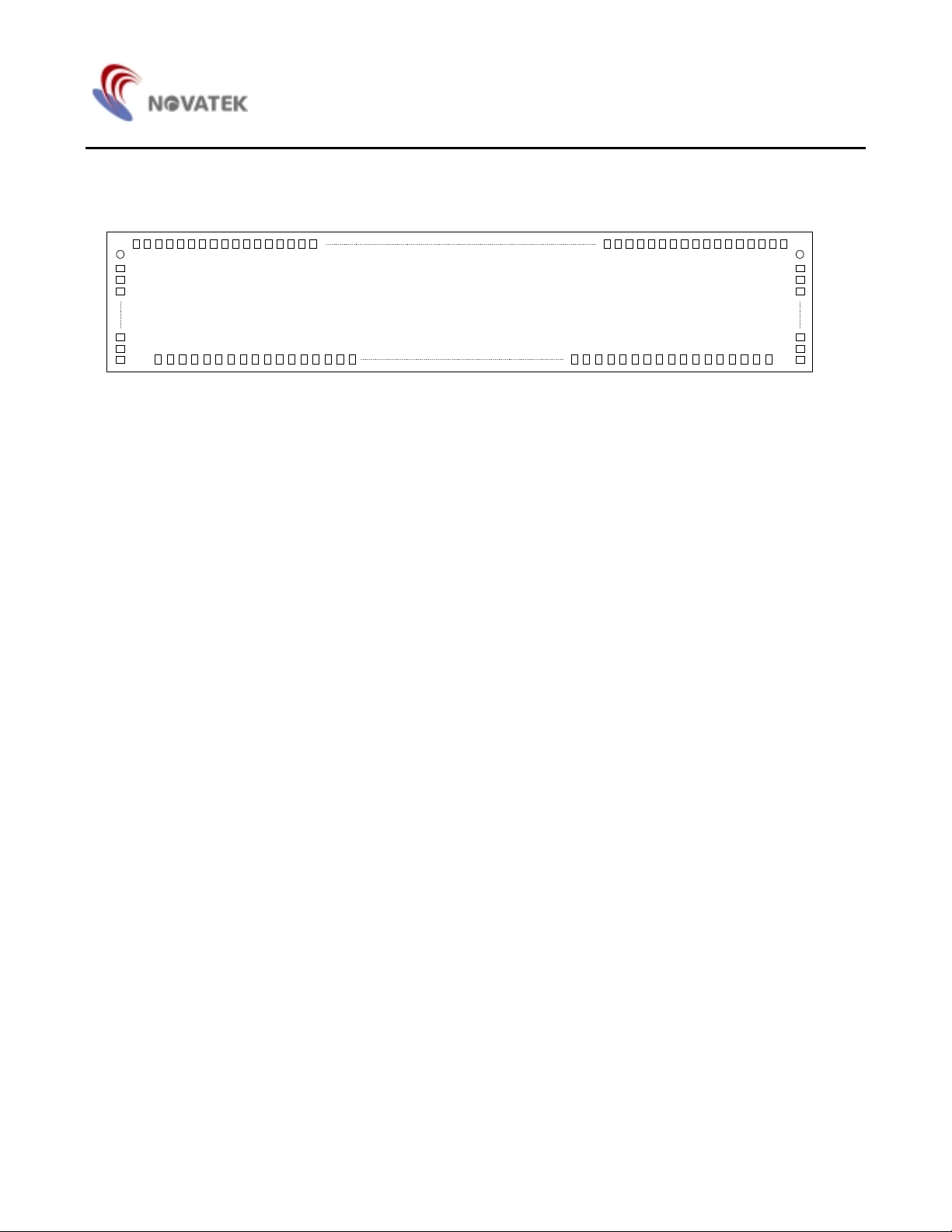
Pad Configuration
198
200
211~199
212
214
180~113
NT7501
18~63
NT7501
98114197 181
97
95
94~82
83
81
64 80117
2
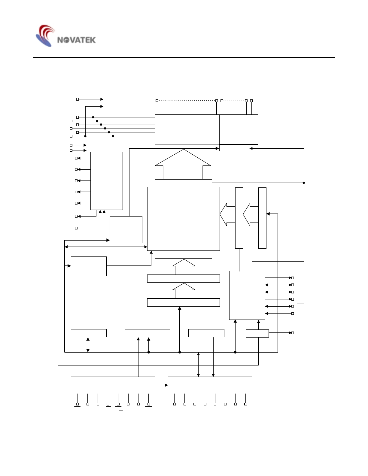
Block Diagram
NT7501
V1
V3
Vss
TPS0
TPS1
CAP1+
CAP1-
CAP2+
CAP2-
CAP3+
V
V
V
DD
0
V
V2
V4
OUT
R
Page address
Power Supply
register
Circuit
Output
status
selector
circuit
SEG0
Segment driver
Display data latch
132*65-dot
display data RAM
I/O buffer circuit
Column address decoder
8-bit column address counter
8-bit column address counter
COM0 COM31 COMS
SEG99
Common
driver
Shift register
line address decoder
Display timing
Line counter
generator
circuit
COM S
Initial display line register
FRS
FR
CL
DYO
DOF
M/S
Bus holder Command decoder Bus holder
Microprocessor interface I/O buffer
CS2 A0
RD
(E)
WR
C86 P/S
)W/R(
RES1CS
(SI)
D7
D5 D4 D3 D2 D1 D0
D6
(SCL)
3
Oscillator
VS1
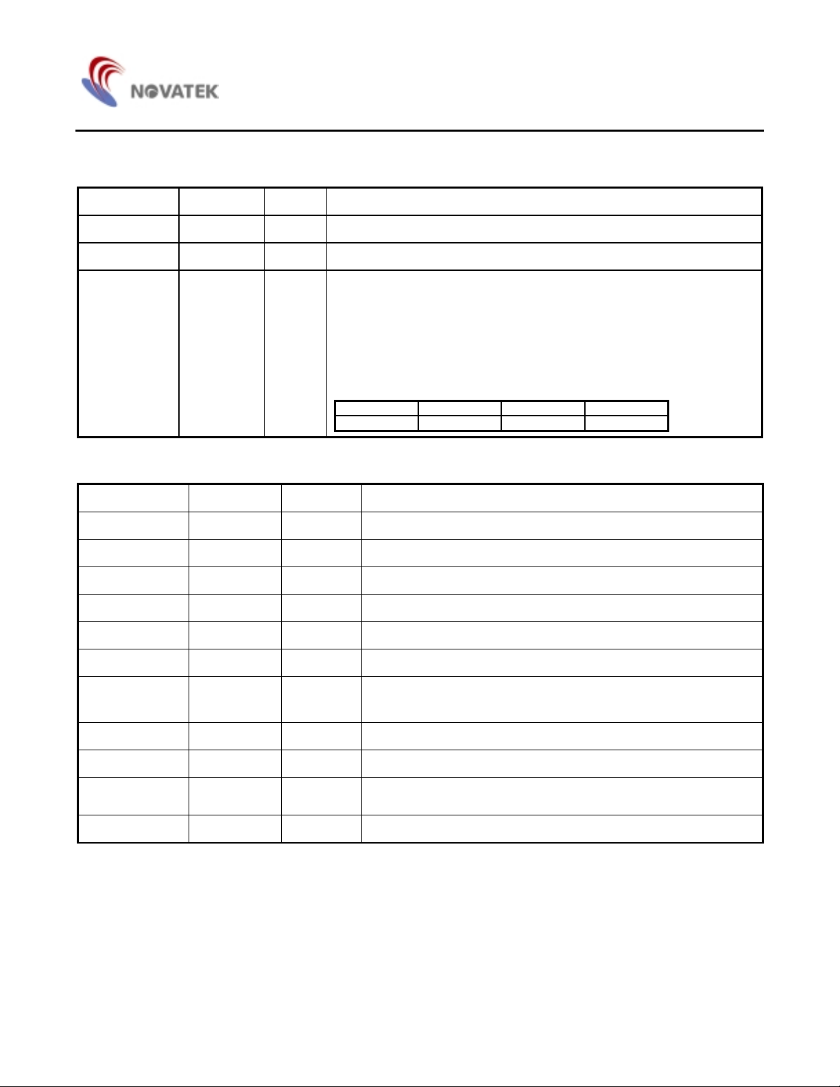
Pad Description
Power Supply
Pad No. Symbol I/O Description
NT7501
20 - 26 V
35 - 42 V
DD
SS
Supply 2.4 - 3.5V power supply input. These pads must be connected to each other
Supply Ground input. These pads must be connected to each other
LCD driver supply voltages. The voltage determined by the LCD cell is
impedance-converted by a resistive driver or an operation amplifier for
63 - 64
65 - 66
67 - 68
69 - 70
71 - 72
V
0
V
1
V
2
V
3
V
4
Supply
application. Voltages should have the following relationship:
V
≥ V2 ≥ V3 ≥ V4 ≥ V
V
≥
0
1
SS
When the on-chip operating power circuit is on, the following voltages are
given to V
to V4 by the on-chip power circuit. Voltage selection is performed
1
by the Set LCD Bias command
V1 V2 V3 V4
4/5V0, 5/6V0 3/5V0, 4/6V0 2/5V0, 2/6V0 1/5V0, 1/6V0
LCD Driver Supplies
Pad No. Symbol I/O Description
47 - 48 CAP1- O Capacitor 1- pad for internal DC/DC voltage converter
49 - 50 CAP1+ O Capacitor 1+ pad for internal DC/DC voltage converter
51 - 52 CAP2- O Capacitor 2- pad for internal DC/DC voltage converter
53 - 54 CAP2+ O Capacitor 2+ pad for internal DC/DC voltage converter
45 - 46 CAP3+ O Capacitor 3+ pad for internal DC/DC voltage converter
12, 61 - 62, 77 V
DD
Supply Used for pad option or to connect to power filter capacitor
9, 15, 59 - 60,
V
SS
Supply Used for pad option or to connect to power filter capacitor
73 - 74
43 - 44 V
55 - 56 V
57 - 58 V
OUT
0
R
O DC/DC voltage converter output
O Connect to Rb
I
Voltage adjustment pad. Applies voltage between V
resistive divider
75 - 76 TPS0, TPS1 I Selects the temperature coefficient of the reference voltage
and VSS using a
0
4
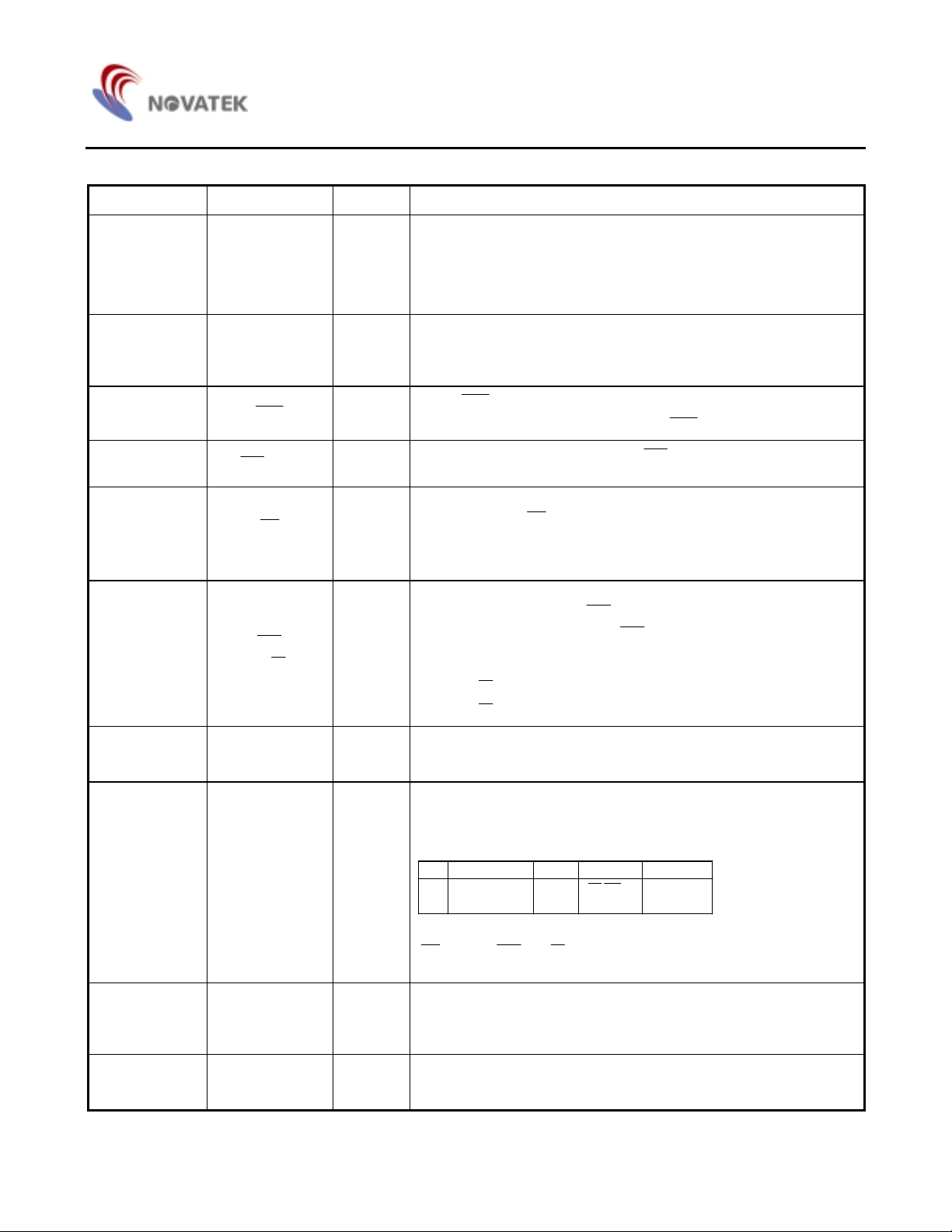
System Bus Connection Terminals
p
Pad No. Symbol I/O Description
This is an 8-bit bi-directio nal dat a bu s that c onn ects to an 8-bit or 16-bit
standard MPU data bus.
When the serial interface is selected (P/S = “L”), then D7 serves as the
serial data input terminal (SI) and D6 serves as the serial clock input
terminal (SCL). At this time, D0 to D5 are set to high impedance.
When the chi
select is inactive, D0 to D7 are set to high impedance.
27 - 34
D0 - D7
(SI)
(SCL)
I/O
This is connected to the l eas t s ign ifi cant bit of the normal MPU addres s
16 A0 I
bus, and it determines whether the data bits are data or a command.
A0 = “H”: Indicate that D0 to D7 are display data.
A0 = “L”: Indicates that D0 to D7 are control data.
When
8
RES
I
RES is set to “L”, the settings are initialized.
The reset operation is performed by the
NT7501
RES signal level.
11 - 13
18
17
1CS CS2
RD
(E)
WR
( WR)
14 C86 I
10 P/S I
I
This is the chip select signal. When
chip select becomes active and data/command I/O are enabled
1CS = “L” and CS2 = “H”, then the
When connected to an 8080 MPU, it is active LOW. This pad is
I
is in an output statue when this signal is “L”.
connected to the
RD signal of the 8080MPU, and the NT7501 data bus
When connected to a 6800 Series MPU, this is active HIGH. This is
used as an enable clock input of the 6800 series MPU.
When connected to an 8080 MPU, this is active LOW. This terminal
connects to the 8080 M PU
latched at the rising edge of the
I
When connected to a 6800 Series MPU: This is the read/write control
WR signal . The signals on the data bus are
WR signal.
signal input terminal.
When
When
WR = “H”: Read.
WR = “L”: Write.
This is the MPU interface switch terminal.
C86 = “H”: 6800 Series MPU interface.
C86 = “L”: 8080 Series MPU interface.
This is the parallel data input/serial data input switch terminal.
P/S = “H”: Parallel data input.
P/S = “L”: Serial data input.
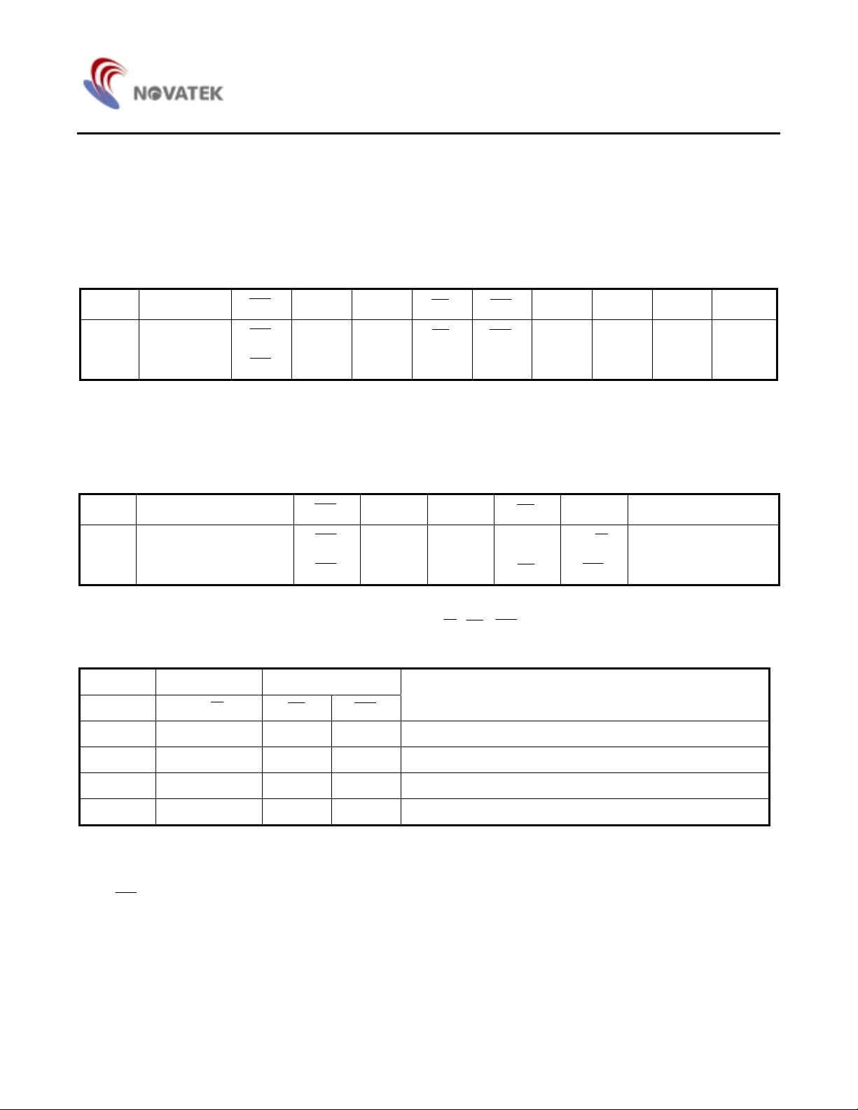
The following applies depending on the P/S status:
P/S Data/Command Data Read/Write Serial Clock
"H" A0 D0 to D 7
"L" A0 SI (D7) Write only SCL (D6)
RDWR
When P/S = “L”, D0 to D5 are HZ. D0 to D5 may be “H”, “L” or Open.
RD(E) and WR ( W/R ) are fixed to either “H” or “L”. With serial data
input, RAM display data reading is not supported.
This terminal selects the master/slave operation for the NT7501 chips.
7M/SI
Master operation outputs the timing signals that are required for the
LCD display, while slav e operatio n input s th e ti ming s ignals require d for
the liquid crystal di splay, synchr onizing the l iquid crystal display sy stem.
This is the display clock input terminal. When the NT7501 chips are
4 CL I/O
used in master/slave mode, the various CL terminals must be
connected.
5

System Bus Connection Terminals (continue)
Pad No. Symbol I/O Description
This is the liquid crystal alternating current signal I/O terminal.
M/S = “H”: Output
2 FR I/O
3DYOO
6 VS1 O Internal power supply voltage monitor output.
5
1FRSO
DOF
I/O
M/S = “L”: Input
When the NT7501 chip is used in master/slave mode, the various FR
terminals must be connected.
Common drive signal output. This output is enabled for only in master
operation and connects to the common driver DIO pad. It becomes HZ
in slave operation.
This is the liquid crystal display blanking control terminal.
M/S = “H”: Output
M/S = “L”: Input
When the NT7501 chip i s used in ma ster/slav e mo de, t he vario us
terminals must be connected
This is the output terminal for the static drive.
This terminal is only enabled when the static indicator is ON when in
master operation mode, a nd is u sed in co njunct ion with th e FR t erminal.
NT7501
DOF
Liquid Crystal Drive Pads
Pad No. Symbol I/O Description
98 - 197 SEG0 - 99 O Segment signal output for LCD display
81 - 96,
198 - 213
97, 214 COMS O
Option Pads
Pad No. Symbol I/O Description
78 - 80 OP1 - OP3 I Internal pull high, no connection for user
COM15 - 0
COM16 - 31
O Common signal output for LCD display
These are the COM output terminals for the indicator. Both terminals
output the same signal.
Do not connect these terminals if they are not used.
When in master/slave mode, the same signa l is output by both master
and slave.
6
NT7501
Functional Description
Microprocessor Interface
Interface type selection
The NT7501 can transfer data via 8-bit bi-directional data bus (D7 to D0) or via serial data input (SI). When high or low is
selected for the parity of the P/S pad, either 8-bit parallel data input or serial data input can be selected as shown in Table 1.
When serial data input is selected, the RAM data cannot be read out.
Table 1.
P/S Type
H Parallel Input
L Serial Input
1CS
1CS
1CS
CS2 A0
CS2 A0
CS2 A0 - - - SI SCL (HZ)
RD WR
RD WR
C86 D7 D6 D0 to D5
C86 D7 D6 D0 to D5
“-” must always be high or low
Parallel Input
When the NT7501 selects parallel input (P/S = high), the 8080 series microprocessor or 6800 series microprocessor can be
selected by causing the C86 pad to go high or low as shown in Table 2.
Table 2.
C86 Type
H 6800 microprocessor bus
L 8080 microprocessor bus
Data Bus Signals
The NT7501 identifies the data bus signal according to A0, E,
Table 3.
Common 6800 processor 8080 processor
A0
1 1 0 1 Reads display data
(
WR)
RD WR
1CS
1CS
1CS
CS2 A0
CS2 A0 E
CS2 A0
WR(RD , W R ) signals.
RD
RD RW
WR D0 to D7
WR
Function
D0 to D7
D0 to D7
1 0 1 0 Writes display data
0 1 0 1 Reads status
0 0 1 0 Writes control data in internal register. (Command)
Serial Interface (P/S is low)
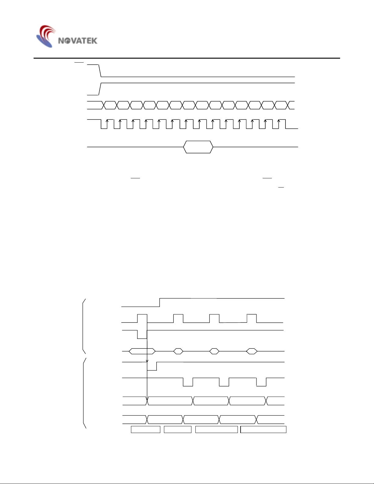
The serial interface consists of an 8-bit shift register a nd a 3-bit co unter. T he serial data input and ser ial cloc k input are enabled
when
The serial data of D7, D6, D0 are read at D7 in this sequenc e when the ser ial clock (SCL) goes high. They are converted into
8-bit parallel data and processed on rising edge of every eighth serial clock signal.
The serial data input (SI) is determined to be the display da ta when A0 is high, and the c ontro l data when A0 is low. A0 is rea d
on the rising edge of every eighth clock signal.
Figure1 shows a timing chart of serial interface signals. The serial clock sign must be terminated correctly against termination
reflection and ambient noise. Operation checkout on the actual machine is recommended.
1CS is low and CS2 is high (in chip select status). When the ch ip is not selecte d, the s hift register and counter are reset.
7
CS
CS2
SI
SCL
A0
Chip Select Inputs
NT7501
1
D7 D6 D5 D4 D3 D2 D1 D0 D7 D6 D5 D4 D3 D2 D1
123456789101112 13 14
Figure 1.
The NT7501 has two chip select pads,
When these pads are set to any other combination, D0 to D7 are high impedance and A0, E and
1CS and CS2 can interface to a microprocessor when 1CS is low and CS2 is high.
WR inputs are disabled.
When the serial input interface is selected. the shift register and counter are reset.
Access to Display Data RAM and Internal Registers
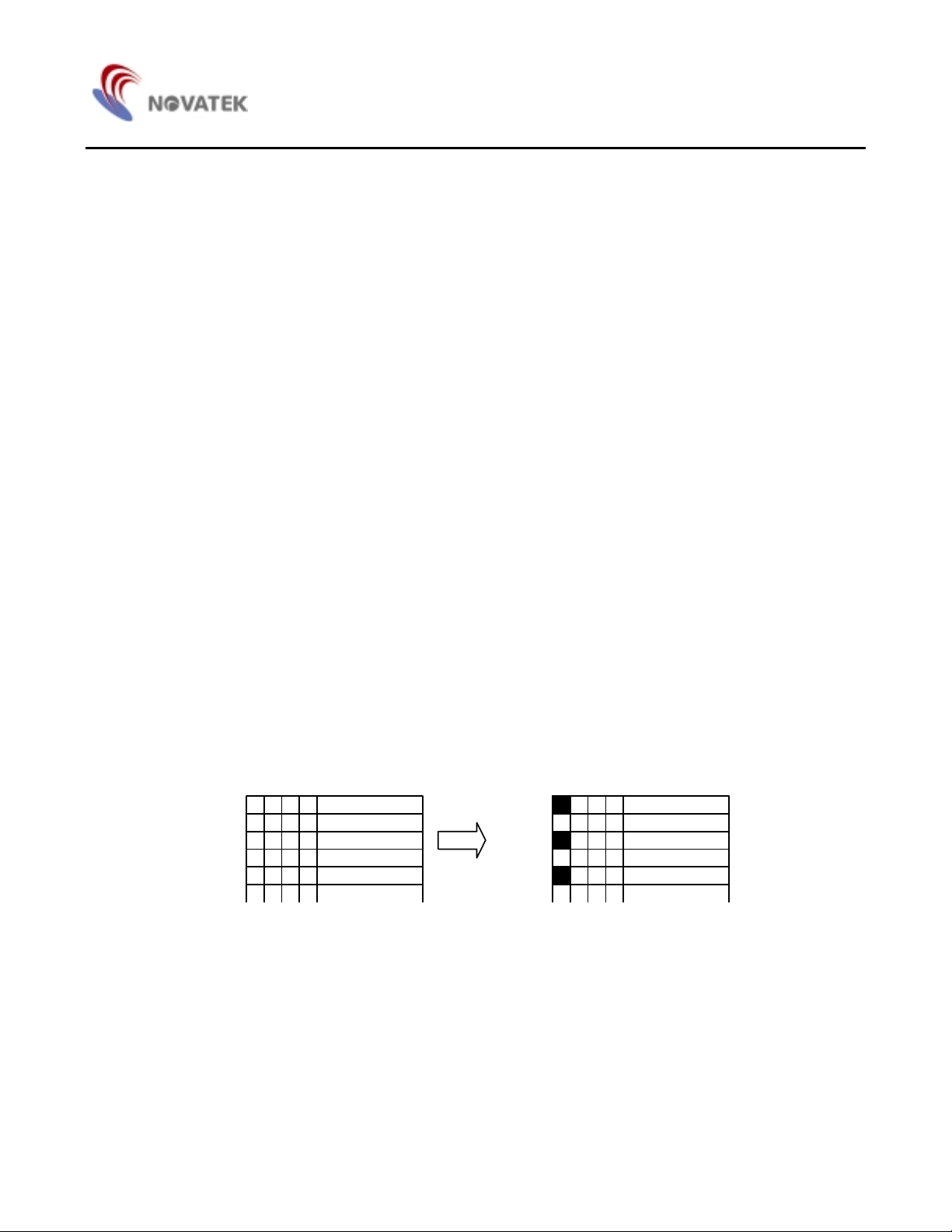
The NT7501 can perform a s eries of pip eline proces ses between t he LSI’s u sing the b us holder of the internal da ta bus in or der
to match the operating fre quency of the display RA M and the inter nal registers w ith that of the microproc essor. For ex ample, the
microprocessor reads data fr om the di splay RA M in the first read (dummy) cycle, stor es it i n the bu s holder and outputs it onto
the system bus in the next data read cycle.
Also, the microprocessor temporarily stores display data in the bus holder, and stores it in the display RAM until the next data
write cycle starts.
When viewed from the microprocessor, the NT7501 access speed greatly depends on the cycle time rather than the access
time to the display RAM (t
). It shows the data transfer speed to/from the microprocessor can increase. If the cycle time is
ACC
inappropriate, the microprocess or can ins ert th e NOP instru ction that is equivalent to the wait cycl e s etup. How ev er, there is a
restriction in the display RAM read sequence. When an address is set, the specified address data is NOT output at the read
instruction immediately follow ing. Inste ad, the a ddress data is output only d uring seco nd data read. A singl e dummy re ad must
be inserted after the address setup and after write cycle (refer to Figure2).
A0
MPU
E
R/W
DATA
N
N
n n+1
Internal
timing
Address preset
Read signal
Column address
BUS holder
Preset
N N+1 N+2
N n n+1
Set address n Dummy read Data Read address n Data Read address n+1
Incremented
n+2
Figure 2.
8
NT7501
Busy Flag
The Busy flag is set when the NT750 1 starts to operate. During oper ation, it ac cepts Read Status instru ction only. The bu sy flag
signal is output at pad D7 w hen Read Status i s issued. If the cy cle time (t
flag before issuing a command. This can greatly improve the microprocessor performance.
Initial Display Line Register
When the display RAM data is read, the display line, according to COM0 (usually, the top line of screen), is determined using
register data. The register is also used for screen scroll ing and pag e sw itch ing.
The set Display Start Line command sets the 6-bit display start address in this register. The register data is preset on the line
counter each time the FR signal stat us change s. The line counter is incremented by C L signal and it gener ates a line addres s to
allow 132 bit.
Column Address Counter
This is a 8 bit presettable cou nter that provid es the colu mn addres s to the display RAM (refer to Figur e4). It is incre mented by 1
when a Read/Write command is entered. However, the counter is not incremented but locked if a non-existing address above
84H is specified. It is unlocked when a column address is set again. The Column Address counter is independent of the Page
Address register.
When the ADC Select command is issued to display an inverse display, the column address decoder inverts the relationship
between the RAM column address and the display segment output.
Page Address Register
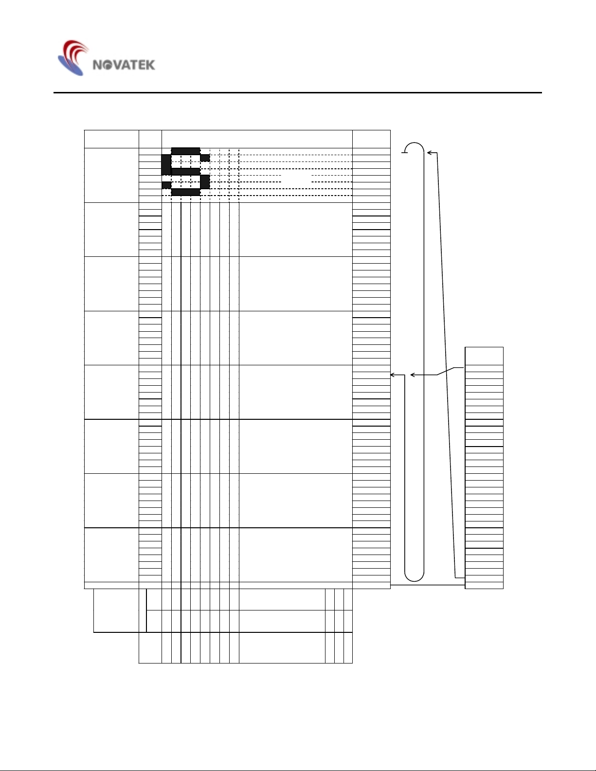
This is a 4-bit page address register that provides a page address to the display RAM (refer to Figure 4). The microprocessor
issues Set Page Address command to change the page and access to another page. Page address 8 (D3 is high, but D2,D1
and D0 are low) is RAM area dedicated to the indicator, and only display data D0 is valid.
) is correct, the micropro cessor nee d not check the
CYC
Display Data RAM
The display data RAM stores pix el data for the LCD . It is a 65-co lumn by 132-row (8-page by 8 bit + 1) addressable array . Each
pixel can be selected when the page and column addresses are specified.
The time required to transfer data i s very short beca use the microproc essor enters D0 to D 7 correspondin g to the LCD common
lines as shown in Figure 3. Therefore, multiple NT7501’s can easily configure a large display having high flexibility with very
little data transmission restriction.
The microprocessor writes and reads data to/from the RAM through the I/O buffer. As the LCD controller operates
independently, data can be written into the RAM at the same time as the data is being displayed, without causing the LCD to
flicker.
D0
D1
D2
D3
D4
1
0
1
0
1
COM0
COM1
COM2
COM3
COM4
Display data RAM Display on LCD
Figure 3.
9
Relationship between display data RAM and address (if initial display line is 21H)
g
NT7501
Page Address Data
D0 00
D1 01
D3,D2,
D1,D0
0,0,0,0
0,0,0,1
0,0,1,0
0,0,1,1
0,1,0,0
0,1,0,1
0,1,1,0
0,1,1,1
1,0,0,0D0 Pa
Column
D2 02
D3 03
D4 04
D5 05
D6 06
D7 07
D0 08
D1 09
D2 0A
D3 0B
D4 0C
D5 0D
D6 0E
D7
D0 10
D1 11
D2 12
D3 13
D4 14
D5 15
D6 16
D7
D0 18
D1 19
D2 1A
D3 1B
D4 1C
D5 1D
D6 1E
D7
D0 20
D1 21
D2 22
D3 23
D4 24
D5 25
D6 26
D7
D0 28
D1 29
D2 2A
D3 2B
D4 2C
D5 2D
D6 2E
D7
D0 30
D1 31
D2 32
D3 33
D4 34
D5 35
D6 36
D7
D0 38
D1 39
D2 3A
D3 3B
D4 3C
D5 3D
D6 3E
D7
101112
“0”
D0=
ADC
address
D0=
737271
”1”
Page0
Page1
Page2
Page3
Page4
Page5
Page6
Page7
e8
717273
121110
Line
Address
0F
17
1F
27
2F
37
3F
Start
COM
output
COM0
COM1
COM2
COM3
COM4
COM5
COM6
COM7
COM8
COM9
COM10
COM11
COM12
COM13
COM14
COM15
COM16
COM17
COM18
COM19
COM20
COM21
COM22
COM23
COM24
COM25
COM26
COM27
COM28
COM29
COM30
COM31
COMS
LCD
OUT
SEG0
SEG1
SEG2
SEG97
SEG98
SEG99
Figure 4.
10
NT7501
Display Timing Generator
This section explains how the display timing generator circuit operates.
Signal Generation to Line Counter and Display Data Latch Circuit
The display clock (CL) generates a clock to the line counter and a latch signal to the display data latch circuit.
The line address of the dis play RAM is generated in sy nchronizatio n with the display clock. 100-bit displ ay data is lat ched by the
display data latch circuit in synchronization with the display clock and output to the segment LCD drive output pad.
The display data is read to the LCD drive circuit completely independent of access to the display data RAM from the
microprocessor.
LCD AC Signal (FR) Generation
The display clock generates an LCD AC signal (FR). The FR causes the LCD drive circuit to generate a AC drive waveform.
It generates a 2-frame AC drive waveform.
When the NT7501 is operated in slave mode on the assumption of multi-chip, the FR pad and CL pad become input pads.
Common Timing Signal Generation
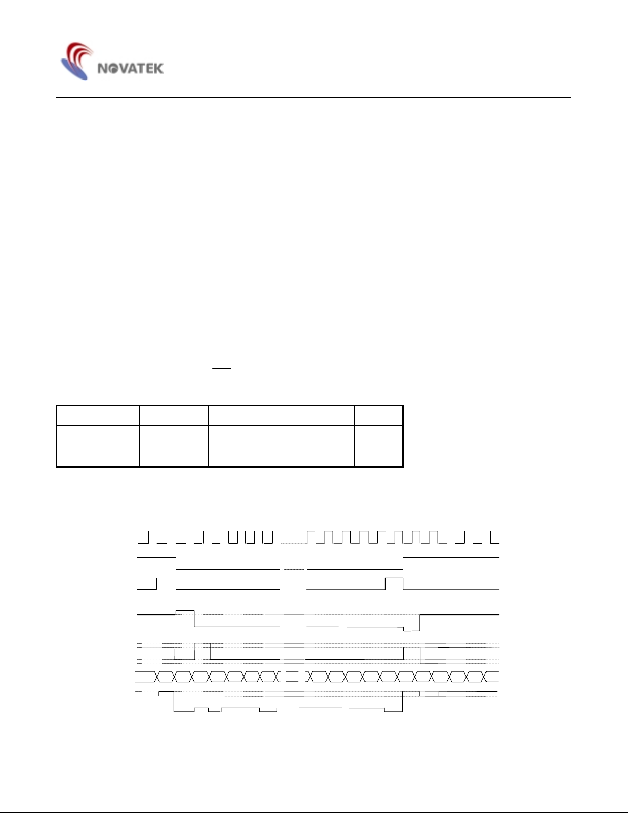
The display clock generates an internal common timing signal and a start signal (DYO) to the common driver. A display clock
resulting from frequency division of an oscillation clock is output from the CL pad.
When an AC signal (FR) is switched, a high pulse is output as a DYO output at the turning edge of the previous display clock.
Refer to Figure 5. The DYO output is output only in master mode.
When the NT7501 is used for multi-chip, the slave requires to receive the FR, CL,
Table 4 shows the FR, CL, DYO and DOFstatus.
DOFsignals from the master.
Table 4.
Model Operation mode FR CL DYO
Master Output Output Output Output
NT7501
Slave Input Input HZ Input
HZ denotes a high-impedance status
Example of NT7501 1/33 duty (Dual-frame AC driver waveforms)
2863332 29 30 31 32 3323451
CL
FR
DYO
COM0
COM1
RAM
data
SEGn
DOF
23451
0
V
V
1
V4
SS
V
0
V
1
V
4
V
SS
V
0
V
2
V
3
V
V
SS
Figure 5.
11

NT7501
Display Data Latch Circuit
This circuit temporarily stores (or latches) display data (during a single common signal period) when it is output from display
RAM to LCD panel driver circuit. This latch is controlled by Display in normal/reverse Display ON/OFF and Entire display on
commands. These commands do not alter the data.
LCD Driver
This is a multiplexer circuit consisting of 100 segment outputs to generate four-level LCD panel drive signals. The LCD panel
drive voltage is generated by a specific combination of display data, a COM scan signal, and a FR signal. Figure 5 gives an
example of SEG and COM output waveform.
Oscillator Circuit
This is an oscillator having a com plete built-i n type CR, and its output is us ed as the display timing signa l source or as the clock
for the voltage booster circuit of the LCD power supply.
The oscillator circuit is available in master mo de only .
The oscillator signal is divided and output as a display clock at the CL pad.
Power Supply Circuit
The power supply circuit generates voltage to drive the LCD panel at low power consumption, and is available in NT7501
master mode only. The power supply circuit cons ists of a volta ge booster, a volt age regulator and a LCD driv e voltage foll ower.
The power supply circuit built in to the NT 7501 is set for a s mall-scale LC D p anel and i s inappropri ate for a large-pix el panel and
a large-display-capacity LCD panel using multipl e chips. A s the lar ge LCD p anel has t he dr opped disp lay qu ality d ue to a large
load capacity, it must use an external power source.
The power circuit is controlled by the Set Power Control command. This command sets a three-bit data in the Power Control
register to select one of ei ght p ower circuit functio ns. T he external power supply a nd p art of the internal pow er circuit functions
can be used simultaneously. The following explains how the Set Power Control command works.
[Control by Set Power Control command]
D2 turns on when the voltage booster control bit goes high, and D2 turns off when this bit goes low.
D1 turns on when the voltage regulator control bit goes high, and D1 turns off when this bit goes low.
D0 turns on when the voltage follower control bit goes high, and D0 turns off when this bit goes low.
[Practical combination examples]
Status 1: To use only the internal power supply
Status 2: To use only the voltage regulator and voltage follower
Status 3: To use only the voltage follower, input the external voltage V
Status 4: To use only an external power supply because the internal power supply does not operate
D2 D1 D0
1 1 1 1 ON ON ON - Used Used
2 0 1 1 OFF ON ON VOUT OPEN Used
3 0 0 1 OFF OFF ON V0 OPEN OPEN
4 0 0 0 OFF OFF OFF V0 to V4 OPEN OPEN
* The voltage booster terminals are CAP1+, CAP1-, CAP2+, CAP2- and CAP3+
* Combinations other than those shown in the above table are possible but impractical.
Voltage
booster
Voltage
regulator
Voltage
follower
0
External
voltage
input
Voltage
booster
terminal
Voltage
regulator
terminal
12
 Loading...