NOVATEK NT7181F, NT7181FQ Datasheet

V 2.1 LVDS Transmitter 24 Bit Color Host-LCD Display Panel Interface
NT7181
NT7181 Specification
V 2.1
NOVATEK MICROELECTRONICS CORP.
1

1 FEATURES .......................................................................................................................................................................3
2 GENERAL DESCRIPTION ............................................................................................................................................ 3
2.1 B
LOCK DIAGRAMS ....................................................................................................................................................... 3
3 PIN CONFIGURATION..................................................................................................................................................4
4 ABSOLUTE MAXIMUM RATINGS .............................................................................................................................5
4.1 R
4.2 T
ECOMMENDED OPERATING CONDITIONS....................................................................................................................5
IMING REQUIREMENTS ...............................................................................................................................................5
5 ELECTRICAL CHARACTERISTICS OVER RECOMMENDED OPERATING CONDITIONS.........................6
6 SWING CHARACTERISTICS OVER RECOMMENDED OPERATING CONDITIONS ....................................7
7 PARAMETER MEASUREMENT INFORMATION....................................................................................................8
8 APPLICATION INFORMATION ...............................................................................................................................12
9 ORDERING INFORMATION .....................................................................................................................................14
10 PACKAGE INFORMATION .......................................................................................................................................15
2

1 Features
! 28:4 Data Channel Compression at up to 297 Megabytes
per Second Throughput
! Suited for VGA, SVGA, XGA and Dual pixel SXGA,
UXGA Display Data Transmission From Controller to
Display With Very Low EMI
! 28 Data Channels and Clock-In Low-Voltage TTL and 4
Data Channels and Clock-Out Low-Voltage Differential
! Operates From a Single 3.3V Supply With 250mW (Typ)
! Low profile 56 Lead TSSOP Package
! Clock edge Programmable for Transmitter
! Wide Phase-Lock Input Frequency Range: 25 MHz To
85 MHz
! Supports Spread Spectrum Clock Generator
! Suggests to use for LCD monitor only
! No External Components Required for PLL
2 General Description
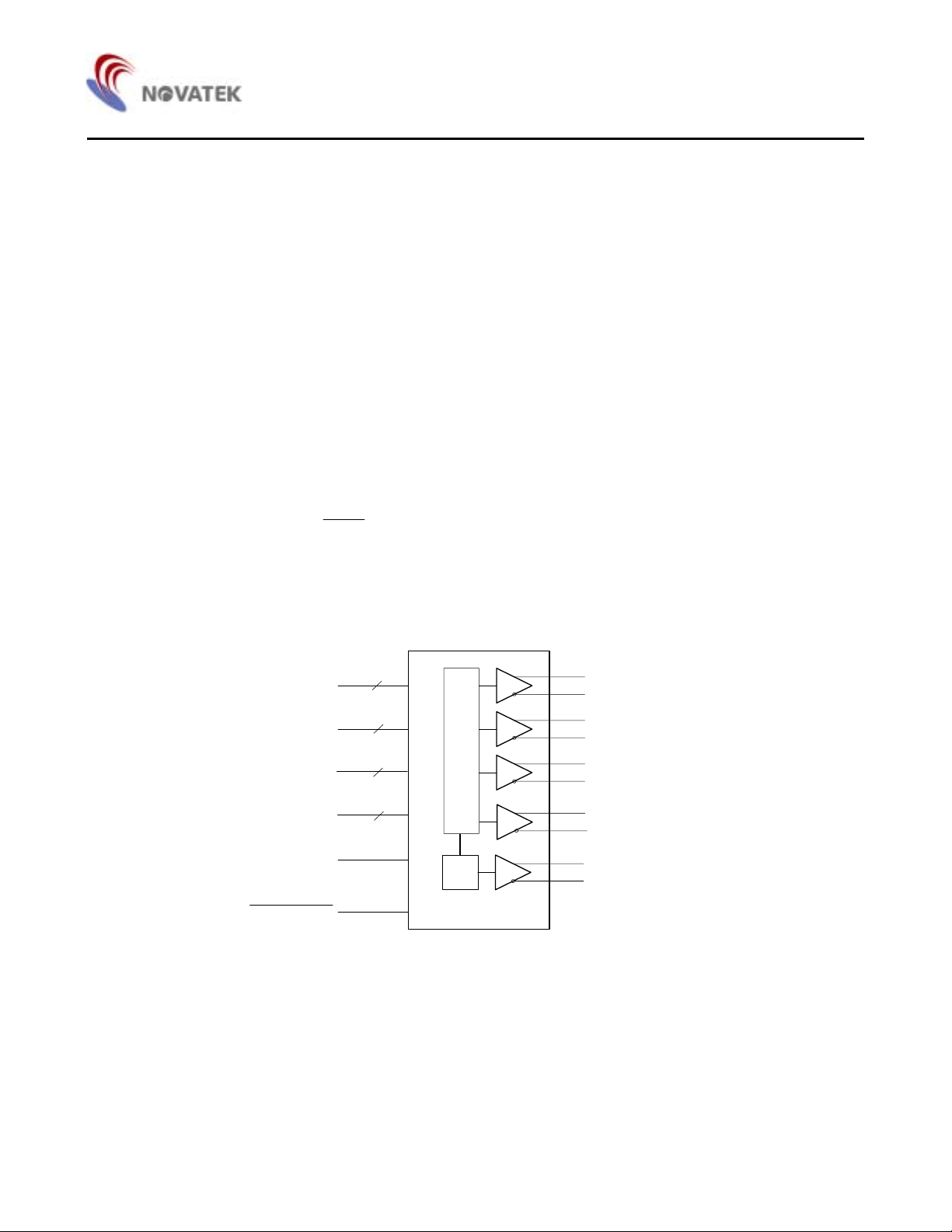
The NT7181 transmitter contains four 7-bit parallel-load serial-out registers, a 7x clock synthesizer, and five low-voltage
differential (LVDS) line in a single integrated circuit. These functions allow 28 bits of single-ended low-voltage TTL (LVTTL)
data to be synchronously transmitted over four balanced-pair conductors for receipt by a compatible receiver, such as the
DS90CF386 or THC63LVDF84A.The NT7181 transmitter is offered with programmable edge data strobes for convenient
interface with a variety of graphic controllers. The NT7181 transmitter can be programmed for rising edge strobe(RFB=1) or
falling edge strobe(RFB=0) through the RFB pin. When transmitting, data bits D0 - D27 are each loaded into registers of the
NT7181 on the rising edge or falling edge of the input clock signal (CLKIN). The frequency of CLKIN is multiplied seven times
and then used to unload the data registers in 7-bit slices and serially. The four serial streams and a phase-locked clock
(TCLK) are then output to LVDS output drivers. The frequency of TCLK is the same as the input clock, CLKIN.
The NT7181 requires no external components and little or no control. The data bus appears the same at the input to the
transmitting and output of the receiver with the data transmission transparent to the user. The only user intervention is the
possible use of the shutdown/clear (
PWDN ) active-low input to inhibit the clock and shut off the LVDS output drivers for
lower power consumption. A low level on this signal clears all internal registers to a low level.
The NT7181 are characterized for operation over free-air temperature ranges of 0°C to 70°C.
2.1 Block Diagrams
NT7181
CMOS / TTL INPUTS
TD0-6
TD7-13
TD14-20
TD21-27
7
7
7
7
T
T
L
P
A
R
A
L
L
E
L
|
T
O
|
L
V
D
S
T0P
T0M
T1P
T1M
T2P
T2M
T3P
T3M
DATA (LVDS)
(175 Mbit/s To 595 Mbit/s On
Each LVDS
Cnannel)
(TRANSMIT CLOCK IN)
(25 MHz To 85 MHz)
POWER DOWN
PLL
TCLKP
TCLKM
CLOCK (LVDS)
(25 MHz To 85 MHz)
3

3 Pin Configuration
NT7181
VCC
TD5
TD6
TD7
GND
TD8
TD9
TD10
VCC
TD11
TD12
TD13
GND
TD14
TD15
TD16
RFB
TD17
TD18
TD19
GND
TD20
TD21
TD22
TD23
VCC
TD24
TD25
1
2
3
4
5
6
7
8
9
10
11
12
13
14
15
16
17
18
19
20
21
22
23
24
25
26
27
28
56
TD4
55
TD3
54
TD2
53
GND
52
TD1
51
TD0
50
TD27
49
LVDSGND
48
T0M
T0P
47
T1M
46
T1P
45
LVDSVCC
44
LVDSGND
43
42
T2M
T2P
41
40
TCLKM
TCLKP
39
T3M
38
T3P
37
LVDSGND
36
35
PLLGND
PLLVCC
34
PLLGND
33
32
PWDN
CLKIN
31
30
TD26
29
GND
4

4 Absolute Maximum Ratings
Supply voltage range, V
Output voltage range, V
Input voltage range, V
Storage temperature range, Tstg……………………………………………………………-65°C to 150°C
Lead temperature 1, 6 mm (1/16 inch) from case for 10 seconds………………………260°C
Junction Temperature…………………………………………………………………………150°C
# Stresses above those listed under "Absolute Maximum Ratings" may cause permanent damage to this device. These are stress
ratings only. Functional operation of this device at these or any other conditions above those indicated in the operational sections of
this specification is not implied or intended. Exposure to the absolute maximum rating conditions for extended periods may affect
device reliability.
CC
(see Note1)……………………………………………………..-0.3V to 4V
O…..……………….…………………………………………………-0.3V to VCC
I……………………………….……………………….…………………………-0.3V to Vcc +0.3V
+0.3V
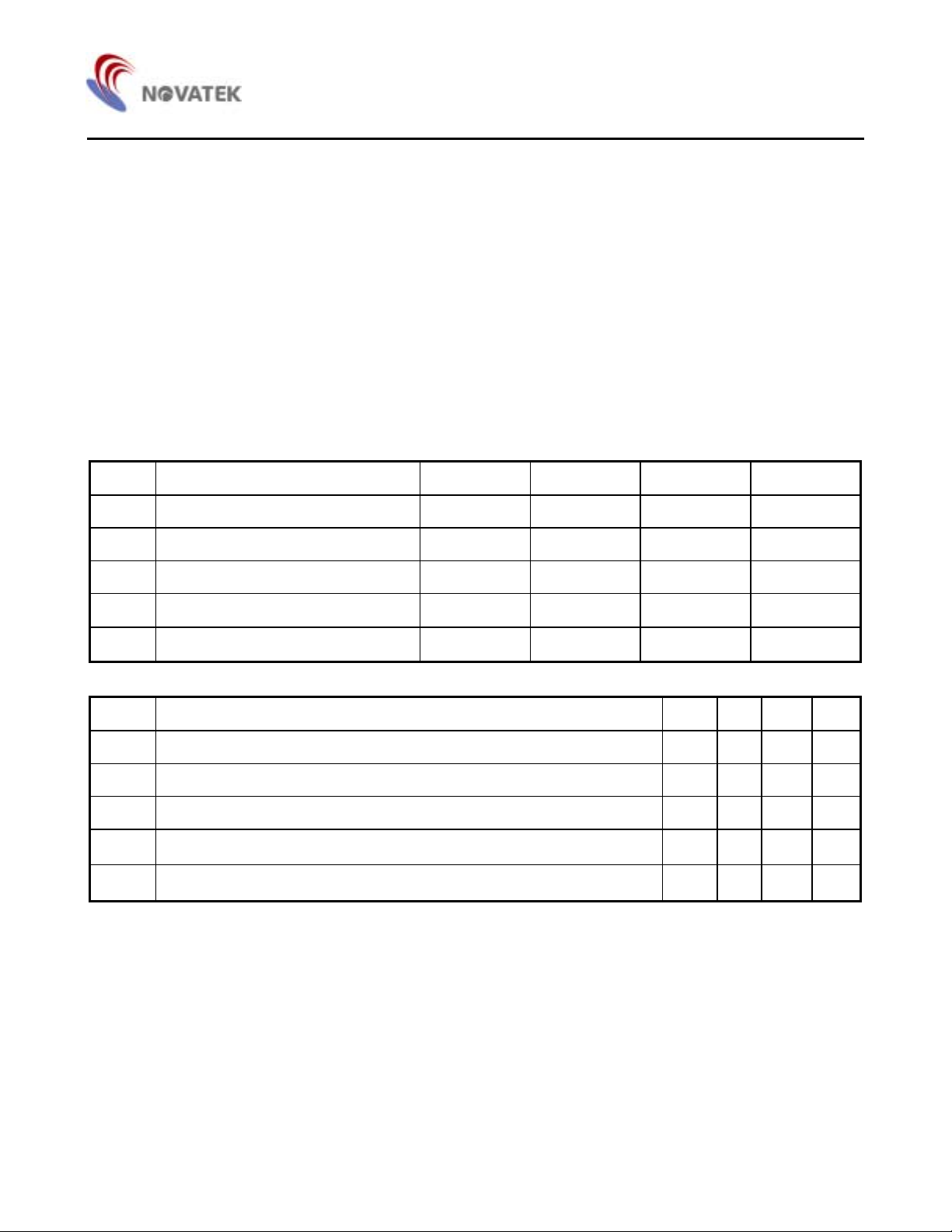
4.1 Recommended Operating Conditions
Symbol Parameter Min. Nom. Max. Unit
VCC Supply voltage 3.0 3.3 3.6 V
VIH High-level input voltage 2 V
VIL Low-level input voltage 0.8 V
ZL Differential load impedance 90 100 110
TA Operating free-air temperature 0 70
Ω
°C
4.2 Timing requirements
Symbol Parameter Min. Nom. Max. Unit
TC Cycle time, input clock 11.8 40 ns
tW Pulse duration, high-level input clock 0.4tc 0.6tc ns
tT Transition, 5 ns
tsu
th
Setup time, data, TD0 - TD27 valid before CLKIN↑or CLKIN ↓ (See Figure 1)
Hold time, data, , TD0 - TD27 valid after CLKIN↑or CLKIN ↓ (See Figure 1)
5 ns
2.5 ns
Note: th is measured under the conditions of input clock jitter of 1.9ns at 65MHz.
5
 Loading...