NOVATEK NT68P81, NT68P81H Datasheet

NT68P81
USB Keyboard Micro-Controller
Features
n Built-in 6502C 8-bit CPU
n 3 MHz CPU operation frequency when oscillator is
running at 6 MHz
n 6K bytes of OTP (one time programming) ROM
n 256 bytes of SRAM
n One 8-bit programmable base timer with pre-divider
circuit
n 29 programmable bi-directional I/O pins including two
external interrupts
n 3 LED direct sink pins with internal serial resistors
n On-chip oscillator (Crystal or Ceramic Resonator)
n Watch-dog timer reset
n Built-in power-on reset
n USB interface
n 3 supported endpoints
n Remote wakeup provided
n CMOS technology for low power consumption
n 40-pin DIP package, 42-pad Dice form and COB
General Description
The NT68P81 is a single chip micro-controller for USB
keyboard applications. It incorporates a 6502C 8-bit
CPU core, 6K bytes of OTP ROM, and 256 bytes of RAM
used as working RAM and stack area. It also includes 29
programmable bi-directional I/O pins with built-in
resistors, and one 8-bit pre-loadable base timer.
Additionally, it includes a built-in power-on reset, a builtin low voltage reset, an oscillator that requires crystal or
ceramic resonator applied, and a watch-dog timer that
prevents system standstill.
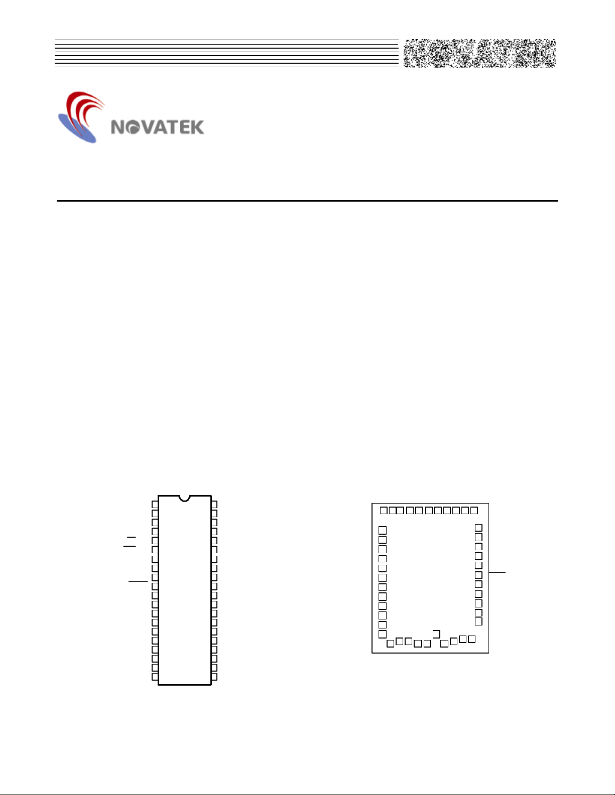
Pin Configuration Pad Configuration
P
1
GND
VCP
VDP
VDM
[OE] P30
[PGM] P31
INT0/P32
INT1/P33
P34
[VPP] RESET
[A0] P00
[A1] P01
[A2] P02
[A3] P03
[A5] P05
[A6] P06
[A7] P07
[A8] P10
[A9] P11
1
2
3
4
5
6
7
8
9
10
11
12
13
14
15
16
17
18
19
20
40
39
38
37
36
35
34
33
NT68P81
32
31
30
29
28
27
26
25
24
23
22
21
OSCI
OSCO
V
DD
LED2 [MODE2]
LED1 [MODE1]
LED0 [MODE0]
P27 [DB7]
P26 [DB6]
P25 [DB5]
P24 [DB4]
P23 [DB3]
P22 [DB2]
P21 [DB1]
P20 [DB0]
P17[A4] P04
P16
P15 [CE]
P14 [A12]
P13 [A11]
P12 [A10]
LED0
LED1
5
25
282726
P16
P17
28
28
P20
29
P21
30
P22
31
P23
32
P24
33
P25
34
34
P26
35
P27
36
37
38
L
E
D
2
P
P
P
P
P
P
1
1
1
4
3
2
24 23 22 21 20 19 18 17
P
1
1
0
0
1
0
7
6
NT68P81
1
4039
O
V
V
S
C
C
C
C
C
O
3
241
42
G
V
O
S
C
I
V
G
N
C
D
N
D
P
P
D
P
0
5
16
P04
15
P03
14
P02
13
P01
12
P00
11
RESET
10
P34
9
P33
8
P32
7
P31
6
P30
5 4
V
D
M
1 V2.0

NT68P81
Block Diagra m
OSCI
OSCO
VDD
GND
RESET
Timing Generator
6502
CPU
Interrupt
Controller
Power-On
Reset
Power Down/Up
6K Bytes
OTP ROM
256 Bytes
SRAM
Watch Dog
Timer
Base Timer
Transceiver
SIE
Serial Bus
Manager
FIFOs
I/O PORTs
VCP
VDP
VDM
LED0
LED1
LED2
P00~P07
P10~P17
P20~P27
P30~P34
2

NT68P81
Pin and Pad Descriptions
Pin No. Pad No. Designation I/O Shared with OTP[I/O]
1 1,2 GND P Ground
2 3 VCP O USB 3.3V driver
3 4 VDP I/O USB data plus
4 5 VDM I/O USB data minus
Bi-directional I/O pin
5 6 P30 I/O
OE [I]
I/O Bi-directional I/O pin
6 7 P31
7 8 P32/INT0 I/O Bi-directional I/O shared with INT0
8 9 P33/INT1 I/O Bi-directional I/O shared with INT1
9 10 P34 I/O Bi-directional I/O pin
PGM [I]
Program output enable
Program control
Description
10 11
11 ~ 18 12 ~ 19
19 ~ 23 20 ~ 24
24 25
25 26
26 27 P17 I/O Bi-directional I/O pin
27 ~ 34 28 ~ 35
35 36
36 37
RESET
VPP [P] Program supply voltage
P00 ~ P07 I/O Bi-directional I/O pin
A0 ~ A7 [I] Program address buffer
P10 ~ P14 I/O Bi-directional I/O pin
A8 ~ A12 Program address buffer
P15 I/O Bi-directional I/O pin
CE [I] Program chip enable
P16 I/O Bi-directional I/O pin
VPIH[I] OTP Program Input Voltage High
P20 ~ P27 I/O Bi-directional I/O pin
DB0 ~ DB7 [I/O] Program data buffer
LED0 O LED direct sink
MODE0 [I] Mode selection
LED1 O LED direct sink
MODE1 [I] Mode selection
I Internally pulled down resistor
37 38
38 39,40 VDD P Power supply (+5V)
39 41
3
LED2 O LED direct sink
MODE2 [I] Mode selection
OSCO O Crystal oscillator output
CLK[I] Program Clock

NT68P81
40 42
* [ ]: OTP Mode
OSCI I Crystal oscillator input
VPIL[I] OTP Program Input Voltage Low
4

NT68P81
Functional De scription
1. 6502C CPU
The 6502C is an 8-bit CPU that provides 56 instructions, decimal and binary arithmetic, thirteen addressing modes, true
indexing capability, programmable stack pointer and variable length stack, a wide selection of addressable memory
range, and an interrupt input. Other features are also included.
The CPU clock cycle is 3MHz (6MHz system clock divided by 2). Please refer to 6502 data sheet for more detailed
information.
07
Accumulator A
7
Index Register Y
7 0
Index Register X
Program Counter PCH
PCL
7 0
7
Stack Pointer SP
N Status Register P
V B D I Z C
0
815
0
07
Carry
Zero
IRQ Disable
Decimal Mode
BRK Command
Overflow
Negative
1 = TRUE
1 = Result ZERO
1 = DISABLE
1 = TRUE
1 = BRK
1 = TRUE
1 = NEG
Figure 1. 6502 CPU Registers and Status Flags
5

NT68P81
2.Instruction Set List
Instruction Code
Meaning Operation
ADC Add with carry A + M + C → A,C
AND Logical AND A•M → A
ASL Shift left one bit C ← M7•••M0 ← 0
BCC Branch if carry clear Branch on C=0
BCS Branch if carry set Branch on C=1
BEQ Branch if equal to zero Branch on Z=1
BIT Bit test A•M,M7 → N,M6 → V
BMI Branch if minus Branch on N=1
BNE Branch if not equal to zero Branch on Z=0
BPL Branch if plus Branch on N=0
BRK Break Forced interrupt PC + 2↓ PC↓
BVC Branch if overflow clear Branch on V=0
BVS Branch if overflow set Branch on V=1
CLC Clear carry 0 → C
CLD Clear decimal mode 0 → D
CLI Clear interrupt disable bit 0 → I
CLV Clear overflow 0 → V
CMP Compare accumulator to memory A - M
CPX Compare with index register X X - M
CPY Compare with index register Y Y - M
DEC Decrement memory by one M - 1 → M
DEX Decrement index X by one X - 1 → X
DEY Decrement index Y by one Y - 1 → Y
EOR Logical exclusive -OR A ⊕ M→A
INC Increment memory by one M + 1 → M
INX Increment index X by one X + 1 → X
INY Increment index Y by one Y + 1 → Y
JMP Jump to new location (PC + 1) → PCL,(PC + 2) → PCH
JSR Jump to subroutine PC + 2↓,(PC + 1) → PCL,(PC + 2) → PCH
6

NT68P81
Instruction Set List (contiuned)
Instruction Code
Meaning Operation
LDA Load accumulator with memory M → A
LDX Load index register X with memory M → X
LDY Load index register Y with memory M → Y
LSR Shift right one bit 0 → M7•••M0 → C
NOP No operation No operation (2 cycles)
ORA Logical OR A + M → A
PHA Push accumulator on stack A ↓
PHP Push status register on stack P ↓
PLA Pull accumulator from stack A ↑
PLP Pull status register from stack P ↑
ROL Rotate left through carry C ← M7•••M0 ← C
ROR Rotate right through carry C → M7•••M0 → C
RTI Return from interrupt P ↑,PC ↑
RTS Return from subroutine PC ↑,PC+1 → PC
SBC Subtract with borrow A - M - C → A,C
SEC Set carry 1 → C
SED Set decimal mode 1 → D
SEI Set interrupt disable status 1 → I
STA Store accumulator in memory A → M
STX Store index register X in memory X → M
STY Store index register Y in memory Y → M
TAX Transfer accumulator to index X A → X
TAY Transfer accumulator to index Y A → Y
TSX Transfer stack pointer to index X S → X
TXA Transfer index X to accumulator X → A
TXS Transfer index X to stack pointer X → S
TYA Transfer index Y to accumulator Y → A
*For more detailed specifications, please refer to 6502 programming data book.
7

NT68P81
3. OTP ROM: 6K X 8 bits
The built-in OTP ROM program code, executed by the 6502 CPU, has a capacity of 6K x 8-bit and is addressed from
E800H to FFFFH. It can be programmed by the universal EPROM writer through a conversion adapter and programming
configuration such as INTEL - 27C64. In the OPERATING mode, the OTP ROM is integrated with the system and it cannot
be directly accessed. When the user wants to work with the OTP ROM alone, the user must first enter the
PROGRAMMING mode by setting: PIN < RESET = VPP>. At this time, through multiplex pins, we can use familiar
procedures to program and verify the OTP ROM block with the universal programmer.
OTP ROM Mega Cell D.C. Electrical Characteristics (READ Mode)
(VDD = 5V, TA = 25℃, unless otherwise specified)
Symbol Parameter Min. Typ. Max. Unit Test Conditions Note
VIH Input Voltage VDD - 0.3 VDD + 0.3
VIL -0.3 0.3 V 1
IIL Input Current +/-10 µA
IOH Output Voltage -400 µA V
IOL 1 mA V
IDD Operating Current 1 mA F = 3MHz 2
I
Standby Current 100 µA 3
STB1
Note: 1. All inputs and outputs are CMOS compatible
2. F = 3MHz, l
= 0mA, CE = VIH. VDD = 5V
out
3. CE = VIH, OE = VIL, VDD = 5V
V 1
= 5V, V OH = 4.5V
DD
= 5V, V OL = 0.5V
DD
OTP ROM Meg a Cell A.C. Electrical Characteristics (READ Mode)
(VDD = 5V, TA = 25℃, unless otherwise specified)
Symbol Parameter Min. Max. Unit Conditions
T
Cycle Time 250 ns
cyc
T12 Non-overlap Time to PH1 & PH2 5 65 ns
T
Address Access Time 145 ns
acc
4.5V < VDD < 5.5V
Tce OTPCE to Output Valid 145 ns
Tst Output Data Setup Time 20 ns
Toh Output Data Hold Time 0 ns
OTP ROM Mega Cell A.C. Test Conditions
Output Load 1 CMOS Gate and CL = 10pF
Input Pulse Rise and Fall Times 10ns Max.
Input Pulse Levels 0V to 5V
Timing Measurement Reference Level Inputs 0V and 5V Outputs 0.3V and 4.7V
8

NT68P81
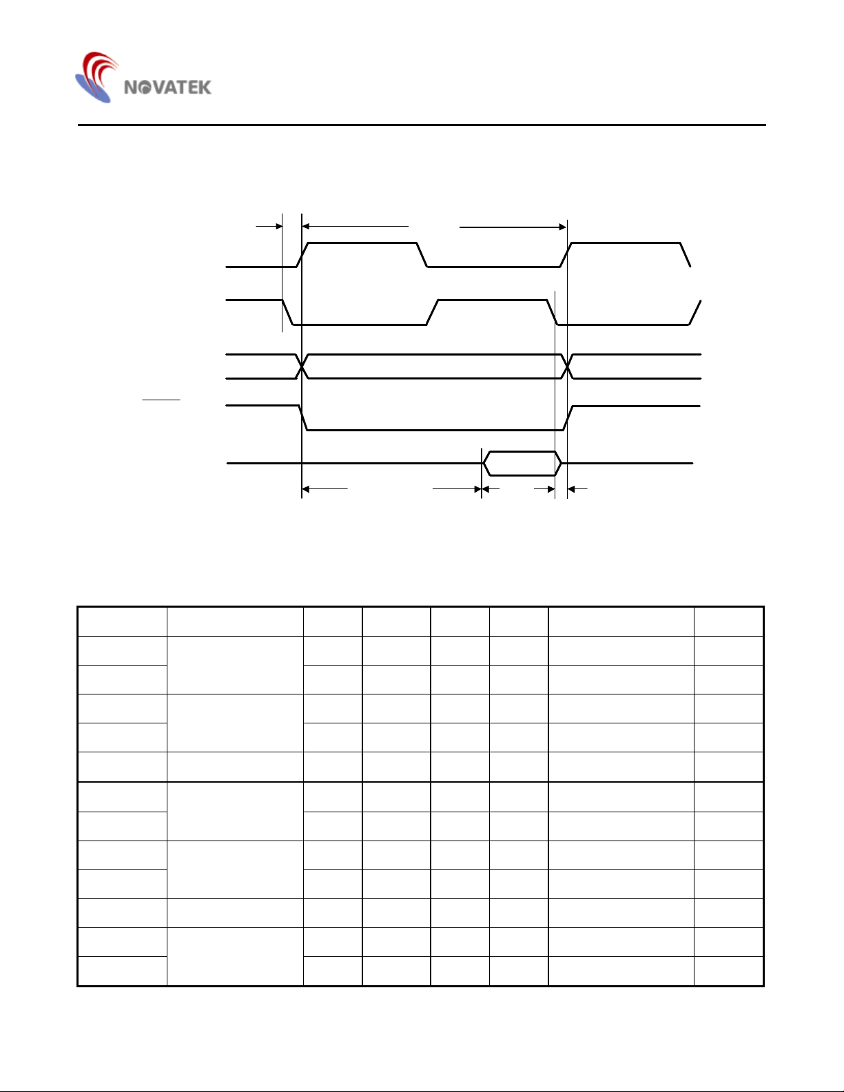
OTP ROM Mega Cell Timing Waveforms (READ mode)
T12
Tcyc
PH1
PH2
A0 - A14
OTPCE
DB0 - DB7
Tacc & Tce Tst
Toh
OTP ROM Mega Cell D.C. Electrical Characteristics (PROGRAMMING Mode)
(VDD = 5V, TA = 25℃, unless otherwise specified)
Symbol Parameter Min. Typ. Max. Unit Test Conditions Note
VDD Supply Voltage 6 6.5 V 4
VPP 10.5 12.75 V
VIH Input Voltage 2 VDD + 0.3
V
VIL -0.3 0.6 V
IIL Output Current +/-10 μA
IOH Output Current -400 μA VDD = 5V, V
IOL 1 mA V
= 5V, V
DD
= 4.5V
OH
= 0.5V
OL
IDD Operating Current 30 mA
IPP 20 mA VPP = 12.75V
CLK Input Clock 53.203424
VPIH Input Voltage 2 VDD + 0.3
MHz
V
VPIL -0.3 0.6 V
9
 Loading...