NOVATEK NT68P61AU, NT68P61A Datasheet
NT68P61A
8-Bit Microcontroller for Monitor (24K OTP ROM Type)
1V1.0
Features
40 pin DIP & 42 pin SDIP package
Operating Voltage Range: 4.5V to 5.5V
CMOS technology for low power consumption
Crystal oscillator or ceramic resonator* available
6502 8-bit CMOS CPU core
8MHz operation of frequency
24K bytes of OTP (one time programming) ROM
256 bytes of RAM (which st ores EDID for DDC1/2B)
One 8-bit pre-loadable base tim er
14 channels of 8 bit PWM outputs:
6 channel with 5V open drain and 8 channel with 12V
open drain
2 channel A/D converters with 6-bit resolution
24 bi-directional I/O port pins and 1 I/P pin
Hsync/Vsync signal processor
Hardware sync signals polarity & fr eq. evaluator
Built-In I
2
C bus interface
Supporting VESA DDC1/2B function
Six-interrupt sources
- INTV (Vsync INT)
- INTE (External INT with ri sing edge trigger)
- INTMR(Ti mer INT )
- INTA (Slave Address Matched INT)
- INTD (Shift Register INT)
- INTS (SCL GO-LOW INT)
Hardware watch-dog timer funct ion
Built-In Low Volt age reset circuit ( LVRC)
General Description
NT68P61A is a moni t or component µC for auto-sync and
digital controlled applications. It contains a 6502
8-bit CPU core, 256 bytes of RAM used as working RAM
and stack area, 24K bytes of OTP ROM**, 14-channel 8bit PWM D/A converters, 2-channel A/D converters for
key detection saving I/O pins, one 8 bit pre-loadable
base timer, internal Hsync and Vsync signal s processor
providing mode detection, watch-dog timer preventing
system from abnormal operation, and an I
2
C bus
interface. The LVRC enables NT68P61A operate
properly.
Users can store EDID data in the 128 bytes of RAM for
DDC1/2B, so th at users can save the cost of dedi cated
EEPROM for EDID. Half frequency output function can
save external one-shot circui t. All of these designs create
savings in component costs.
* The frequency deviation of ceramic resonator has
+/- 6% maximum.
** The NT6861 (MASK ROM type) will provide
4/8/12/16/24K bytes program ROM.
NT68P61A
2
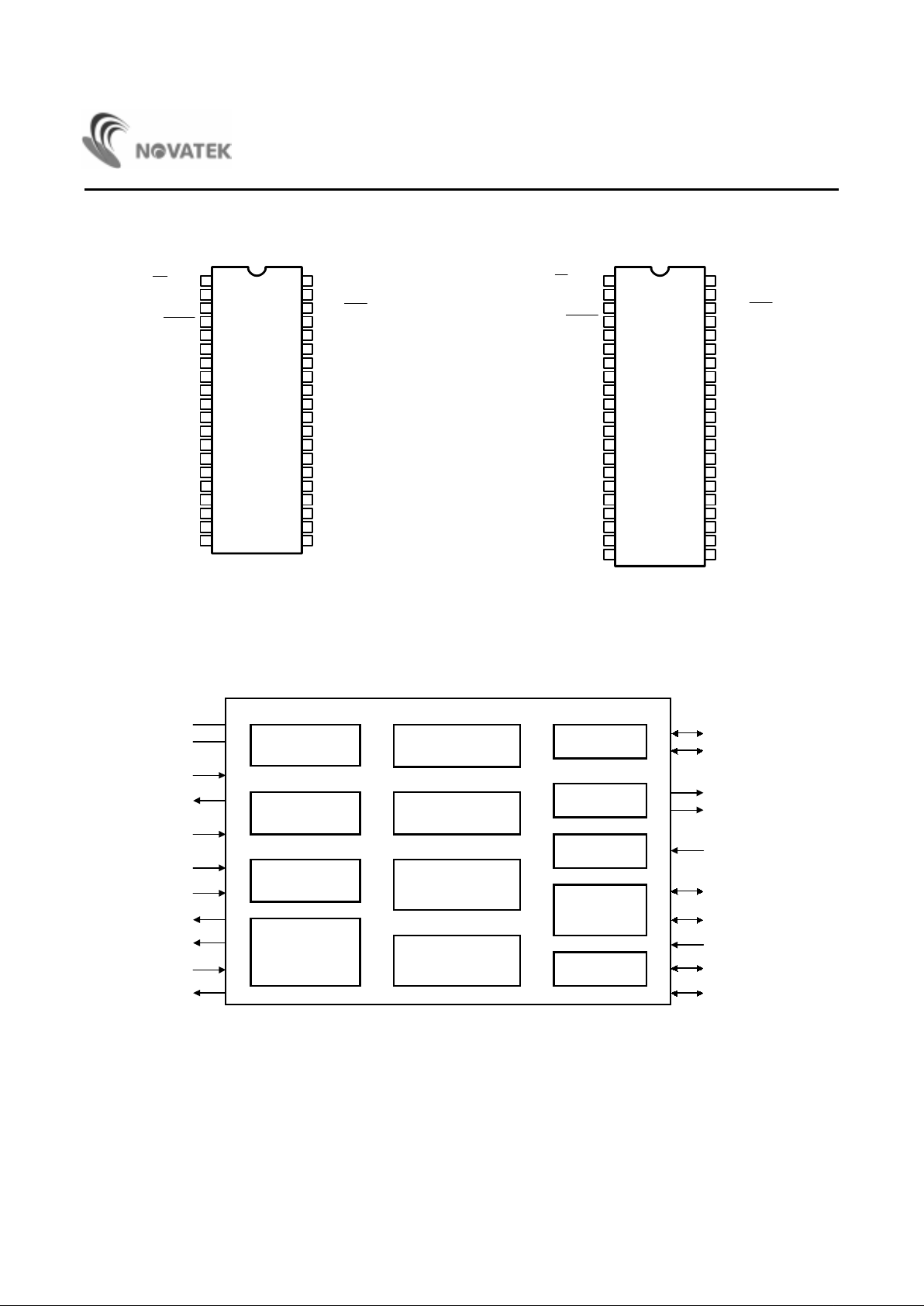
Pin Configuration
[OE] DAC2
DAC1
DAC0
[DB7] P27
[VPP] RESET
V
DD
GND
OSCO
OSCI
[CE] P14
[A10] P12/HALFHO
[A9] P11/AD1
[A8] P10/AD0
P20 [DB0]
P07/HSYNCO [A7]
P31/SCL [A13]
DAC4 [MODE0]
DAC3 [PGM]
HSYNCI
VSYNCI/INTV/ [A14]
NT68P61A
1
2
3
4
5
6
7
8
9
10
11
12
13
14
15
16 25
26
27
28
29
30
31
32
33
34
35
36
37
38
39
40
P15
[A11] P13/HALFHI
P16/INTE
17
18
19
20
24
23
22
21
DAC5 [MODE1]
DAC6 [MODE2]
DAC7
P21 [DB1]
P22 [DB2]
P06/VSYNCO [A6]
P05/DAC13 [A5]
P04/DAC12 [A4]
P03/DAC11 [A3]
P02/DAC10 [A2]
P01/DAC9 [A1]
P00/DAC8 [A0]
P30/SDA [A12]
[DB6] P26
[DB5] P25
[DB4] P24
[DB3] P23
* [ ]: OTP Mode
[OE] DAC2
DAC1
DAC0
[VPP] RESET
V
DD
NC
GND
OSCO
OSCI
P15
[A11] P13/HALFHI
[A9] P11/AD1
[A8] P10/AD0
P00/DAC8 [A0]P16/INTE
P01/DAC9 [A1]
P02/DAC10 [A2]
P03/DAC11 [A3]
P04/DAC12 [A4]
P06/VSYNCO [A6]
P07/HSYNCO [A7]
DAC6 [MODE2]
NC
DAC5 [MODE1]
DAC4 [MODE0]
DAC3 [PGM]
HSYNCI
VSYNCI/INTV
DAC7 [A14]
NT68P61AU
1
2
3
4
5
6
7
8
9
10
11
12
13
14
15
16 27
28
29
30
31
32
33
34
35
36
37
38
39
40
41
42
[CE] P14
[A10] P12/HALFHO
[DB7] P27
[DB6]P26
[DB5] P25
[DB4] P24
[DB3] P23
17
18
19
20
21
P05/DAC13 [A5]
P31/SCL [A13]
P30/SDA [A12]
P20 [DB0]
P21 [DB1]
P22 [DB2]
26
25
24
23
22
* [ ]: OTP Mode
Block Diagram
Timing Generator
CPU core
6502
Interrupt
Controller
H/V Sync Signals
Processor
SRAM + STACK
256 Bytes
Watch Dog Timer
PWM DACs
I/O Ports
OSCI
OSCO
V
DD
GND
HSYNCI
INTE
SCL
SDA
DAC0 - DAC7
P00 - P07
P10 - P15
P20 - P27
VSYNCO
A/D Converter
AD0 - AD1
8 Bit Base Timer
P30 - P31
IIC BUS
P16
HSYNCO
HALFHI
HALFHO
DAC8 - DAC13
VSYNCI/INTV
OTP Program ROM
24K Bytes
LVRC
NT68P61A
3
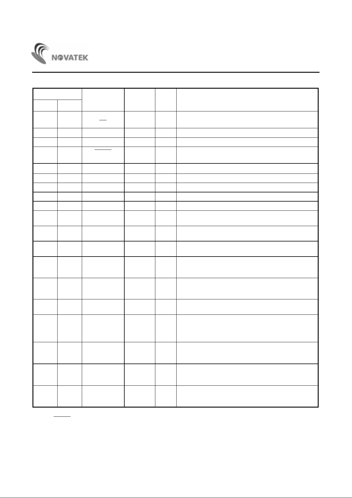
Pin Descrip t ions
Pin No.
Designation Reset Init. I/O Description
40 Pin 42 Pin
1 1 DAC2
[
OE
]
O
[ I ]
Open drain 12V, D/A converter output 2
[OTP ROM program out put enable]
2
2 DAC1 O Open drain 12V, D/A converter output 1
3 3 DAC0 O Open drain 12V, D/A converter output 0
44
RESET
[ VPP ]
I
[ P ]
Schmitt t r igger input pin, low acti ve reset**
[OPT ROM program suppl y voltage]
55
V
DD
PPower
6 7 GND P Ground
7 8 OSCO O Crystal OSC output
8 9 OSCI I Crystal OSC input
9 10 P15 I/O Bi- directional I/O pin
10 11 P14
[ CE ]
I/O
[ I ]
Bi- directional I/O pin
[OTP ROM program chip enable]
11 12 P13/HALFHI
[ A11 ]
P13 I/O
[ I ]
Bi- directional I/O pin, shared with half hsync input
[OTP ROM program addr ess buffer]
12 13 P12/HALFHO
[ A10 ]
P12 I/O
[ I ]
Bi- directional I/O pin, shared with half hsync output
[OTP ROM program addr ess buffer]
13 14 P11/AD1
[ A9 ]
P11 I/O
[ I ]
Bi- directional I/O pin, shared with A/D converter channel
1 input
[OTP ROM program addr ess buffer]
14 15 P10/AD0
[ A8 ]
P10 I/O
[ I ]
Bi- directional I/O pin, shared with A/D converter
channel 0 input
[OTP ROM program addr ess buffer]
15 16 P16/INTE P16 I Schmitt trigger input pin with internal pul l high, shared
with external Rising-edge trigger interrupt
16 - 23 17 - 24 P27 - P20
[ DB7 ] -
[ DB0 ]
I/O
[ I/O ]
Bi- directional I/O pin, push-pull structure with high current
drive/sink capability
[OTP ROM program dat a buf fer]
24 25 P30/SDA
[ A12 ]
P30 I/O
[ I ]
Open drain 5V Bi-direction I/O pin P30, shared with SDA
pin of I
2
C bus schmitt trigger buffer
[OTP ROM program addr ess buffer]
25 26 P31/SCL
[ A13 ]
P31 I/O
[ I ]
Open drain 5V Bi-direction I/O pin P31, shared with SCL
pin of I
2
C bus schmitt trigger buffer
[OTP ROM program addr ess buffer]
26 27 P00/DAC8
[ A0 ]
P00 I/O
[ I ]
Bi- directional I/O pin, shared with open drain 5V D/A
converter output 8
[OTP ROM program addr ess buffer]
* [ ]: OTP Mode
** This
RESET
pin must be pull ed high by external pulled-up resistor ( 5KΩ suggestion), or it will stay low
voltage to reset system all the tim e.

NT68P61A
4
Pin Descrip t ions (con t inued)
Pin No.
Designation Reset Init. I/O Description
40 Pin 42 Pin
27 28 P01/DAC9
[ A1 ]
P01 I/O
[ I ]
Bi- directional I/O pin, shared with open drain 5V D/A
converter output 9
[OTP ROM program addr ess buffer]
28 29 P02/DAC10
[ A2 ]
P02 I/O
[ I ]
Bi- directional I/O pin, shared with open drain 5V D/A
converter output 10
[OTP ROM program addr ess buffer]
29 30 P03/DAC11
[ A3 ]
P03 I/O
[ I ]
Bi- directional I/O pin, shared with open drain 5V D/A
converter output 11
[OTP ROM program addr ess buffer]
30 31 P04/DAC12
[ A4 ]
P04 I/O
[ I ]
Bi- directional I/O pin, shared with open drain 5V D/A
converter output 12
[OTP ROM program addr ess buffer]
31 32 P05/DAC13
[ A5 ]
P05 I/O
[ I ]
Bi- directional I/O pin, shared with open drain 5V D/A
converter output 13
[OTP ROM program addr ess buffer]
32 33 P06/VSYNCO
[ A6 ]
P06 I/O
[ I ]
Bi- directional I/O pin, shared with vsync out
[OTP ROM program addr ess buffer]
33 34 P07/HSYNCO
[ A7 ]
P07 I/O
[ I ]
Bi-directional I/O pin, shared with hsync out
[OTP ROM program addr ess buffer]
34 35 DAC7
[ A14 ]
O Open drain 12V, D/A converter output
[OTP ROM program addr ess buffer]
35 36 DAC6
[ MODE2 ]
O
[ I ]
Open drain 12V, D/A converter output
[OTP ROM mode select]
36 38 DAC5
[ MODE1 ]
O
[ I ]
Open drain 12V, D/A converter output
[OTP ROM mode select]
37 39 DAC4
[ MODE0 ]
O
[ I ]
Open drain 12V, D/A converter output
[OTP ROM mode select]
38 40 DAC3
[
PGM
]
O
[ I ]
Open drain 12V, D/A converter output
[OTP ROM program control]
39 41 HSYNCI I Debouncing & schmitt t r i gger input pin for video horizontal
sync signal, int ernal pul l high, shared with composi te sync
input
40 42 VSYNCI/INTV
[A14]
VSYNCI I
[ I ]
Debouncing & schmitt tr igger input pin for video vertical
sync signal, int ernal pull high, shared with external
interrupt source
- 6 NC I/O
Bi-directional I/O pin, with internal pulled up 22K
Ω
resister, only 42 pin SDIP available
- 37 NC I/O
Bi-directional I/O pin, with internal pulled up 22K
Ω
resister, only 42 pin SDIP available
* [ ]: OTP Mode
NT68P61A
5
Functional Descriptions
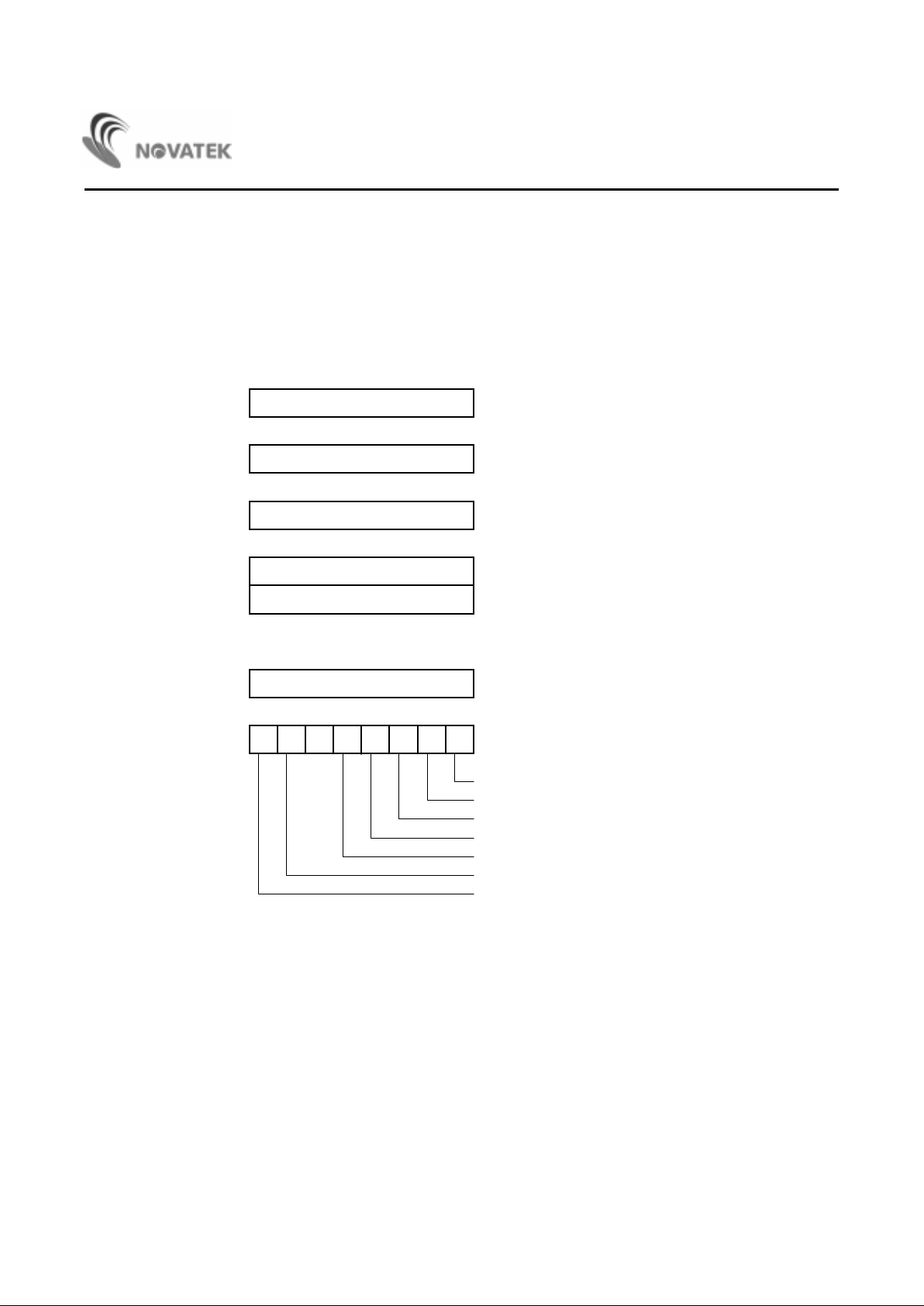
1. 6502 CPU
The 6502 is an 8-bit CPU that provides 56 instructions, decimal and binar y arithmetic, thir teen addressing modes, true
indexing capability, programmable stack pointer with variable length stack, a wide selection of addressable memory, and
interrupt input opt i ons.
The CPU clock cycle is 4MHz (8MHz system clock divided by 2). Refer to 6502 data sheet for more details.
Accumulator A
Index Register Y
07
7
Index Register X
70
0
Stack Pointer SP
0
N Status Register P
07
Carry
Zero
IRQ Disable
Decimal Mode
BRK Command
Overflow
Negative
7
Program Counter PCH
8
15
70
PCL
1 = TRUE
1 = Result ZERO
1 = DISABLE
1 = TRUE
1 = NEG
1 = TRUE
1 = BRK
VBDIZ
C
Figure 1. 6502 CPU Registers and Stat us Fl ags
NT68P61A
6
2. Instruction Set List
Instruction Code Meaning Operation
ADC Add with carry A + M + C → A, C
AND Logical AND A • M → A
ASL Shift left one bit C ← M7
• •
•
M0 ← 0
BCC Branch if carry clears Branch on C = 0
BCS Branch if carry sets Branch on C = 1
BEQ Branch if equal to zero Branch on Z = 1
BIT Bit test A • M, M7
→
N, M6
→
V
BMI Branch if m i nus Branch on N = 1
BNE Branch if not equal to zero Branch on Z = 0
BPL Branch if plus Branch on N = 0
BRK Break Forced Interrupt PC+2 ↓ PC
↓
BVC Branch if overflow clears Branch on V = 0
BVS Branch if overflow sets Branch on V = 1
CLC Clear carry 0 → C
CLD Clear decimal mode 0 → D
CLI Clear interrupt disable bit
0 →
J
CLV Cl ear overflow 0 → V
CMP Compare accumulat or t o memory A − M
CPX Compare with index register X X − M
CPY Compare with index register Y Y − M
DEC Decrement m emor y by one M − 1 → M
DEX Decrement index X by one X − 1 → X
DEY Decrement index Y by one Y − 1
→
Y
EOR Logical exclusive-OR A ⊕ M
→
A
INC Increment memory by one M + 1 → M
INX Incr em ent i ndex X by one X + 1 → X
INY Incr em ent i ndex Y by one Y + 1 → Y
NT68P61A
7
Instruction Set List (continued)
Instruction Code Meaning Operation
JMP Jump to new location (PC+1)
→
PCL, (PC+2)
→
PCH
JSR Jump t o subr out ine PC + 2 ↓, (P+1)
→
PCL, (PC+2)
→
PCH
LDA Load accumulator with memory M → A
LDX Load Index register X with memory M → X
LDY Load Index register Y with memory M → Y
LSR Shift right one bit 0 → M7
• • •
M0
→
C
NOP No operation No operation (2 cycles)
ORA Logical OR A + M
→
A
PHA Push accumul at or on st ack A
↓
PHP Push status register on stack P
↓
PLA Pull accum ulator from st ack A
↑
PLP Pull status r egist er from stack P
↑
ROL Rotat e left t hr ough car r y C ← M7
• • •
M0 ← C
ROR Rotate right through carry C → M7
• • •
M0 → C
RTI Return from i nt errupt P ↑, PC
↑
RTS Return fr om subroutine PC ↑, PC+1 → PC
SBC Subtract wit h bor r ow A − M − C → A, C
SEC Set car ry 1 → C
SED Set decimal mode 1
→
D
SEI Set interrupt disable status
1 →
J
STA Store accumulator in memory A → M
STX Store index register X in memory X → M
STY Store index register Y in memory Y → M
TAX Transfer accumulator to index X A
→
X
TAY Transfer accumulator to index Y A → Y
TSX Transfer stack pointer to index X S → X
TXA Transfer index X to accumulator X → A
TXS Transfer index X to stack Pointer X
→
S
TYA Transfer index Y to accumulator Y → A
* Refer to 6502 programming data book for more details.
NT68P61A
8
3. OT P ROM: 24K X 8 bits
The OTP ROM storing applic ation program code, executed by 6502 CPU, has a capacity of 24K X 8 bits, addressed from
$A000 to $FFFF. It i s pr ogr ammed by the universal EPROM writ er thr ough a conversion adapter.
In PROGRAMMING mode, OTP ROM is i ntegrated with system and cannot be directly accessed. When using the OTP
ROM alone, first enter the PROGRAMMING mode by setting:
RESET
= VPP.
At this tim e, through m ultiplex pins, normal procedures are used to program and verify the OTP ROM block with the
universal program mer.
OTP ROM Mega Cell D.C. Electri cal Characteristics (READ M ode)
(VDD = 5V , TA = 25°C, unless otherwise specified)
Symbol Parameter Min. Typ. Max. Uni t Test Conditions Note
V
IH
VDD-0.3 VDD+0.3
V1
V
IL
Input Voltage
-0.3 0.3 V 1
I
IL
Input Current +/-10
µ
A
I
OH
-400
µ
A
V
DD
=5V, VOH = 4.5V
I
OL
Output Voltage
1
µ
A
V
DD
=5V, VOL = 0.5V
I
DD
Operating Current 1
µ
A
f = 4MHz 2
ISTB1 Standby Curr ent 100
µ
A
3
Notes: 1. All inputs and outputs are CMOS compatible
2. f = 4MHz, Iout = 0mA, CE = V
IH
, VDD = 5V
3. CE = V
IH
, OE = VIL, VDD = 5V
OTP ROM Mega Cell l A.C. Electr ical Characteristics ( READ M ode)
(V
DD
= 5V, TA = 25°C, unless otherwise specified)
Symbol Parameter Min. Max. Unit Conditions
Tcyc Cycle Time 250 ns
T12 Nonoverlap Time to PH1 & PH2 5 65 ns
Tacc
Address Access Time
145 ns
Tce
OTPCE to Output Valid
145 ns
4.5V < V
DD
< 5.5V
Tst
Output Data Setup Time
20 ns
Toh Output Data Hol d Time 0 ns
OTP ROM MEGA CELL A.C. Test Condit i ons
Output Load 1 CMOS Gate and CL = 10pF
Input Pulse Rise and Fall Times 10ns Max.
Input Pulse Levels 0V to 5V
Timing Measurement Reference Level Input s 0V and 5V out put s 0. 3V and 4. 7V
NT68P61A
9
OTP ROM Mega Cell Timing Waveforms (READ Mode)
Tcyc
T12
Tacc & Tce Tst
Toh
PH1
PH2
A0 - A14
OTPCE
DB0 - DB7
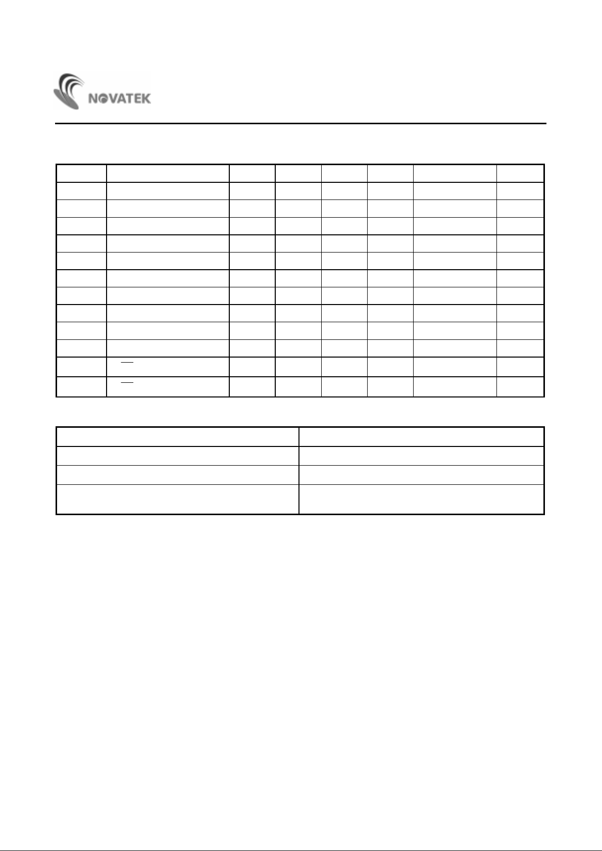
OTP ROM Mega Cell A.C. Electri cal Characteristics (PRO G RAMMING Mode)
(T
A
= 25°C, unless otherwise specified)
Symbol Parameter Min. Typ. M ax. Unit Test Conditions Note
V
DD
Supply Voltage 6 6. 5 V 4
VPP 10.5 12. 75 V
V
IH
Input Voltage 2
V
DD
+0.3
V
V
IL
-0.3 0.8 V
IIL Input Current +/-10
µ
A
I
OH
Output Current - 400
µ
A
V
DD
= 5V, VOH = 4.5V
I
OL
1mA
V
DD
= 5V, VOL = 0.5V
I
DD
Programming 30 mA
IPP Current 20 m A VPP = 12.75V
Note: 4. For reliability concern, we suggested VDD = 6V & VPP = 12.75V for test OTP ROM AC characterist ics in
PROGRAMMING mode, using the same conditi on f or t he universal pr ogr ammer supply volt age.
NT68P61A
10
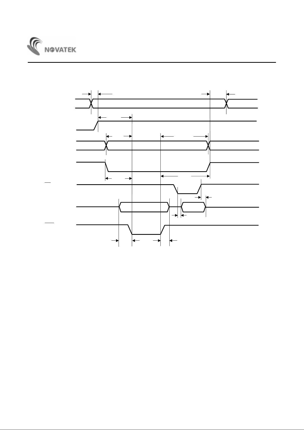
OTP ROM Mega Cell D.C. Electri cal Characteristics (PROGRAMMING Mode)
(T
A
= 25°C, unless otherwise specified)
Symbol Paramet e r Min. Typ. Max. Unit Test Condit ions Note
Tms Mode Decode Setup Time 2
m
s
Tmh Mode Decode Hold Time 2
m
s
Tas Address Setup Time 2
m
s
Tah Address Hold Time 2
m
s
Tces CE Setup Time 2
m
s
Tceh CE Hold Tim e 2
m
s
Tds Data Setup Time 2
m
s
Tdh Data Hold Time 2
m
s
Tvs VPP Setup Time 2
m
s
Tpw Program Pul se Width 100
m
s
Tdv
OE
to Output Valid
150
n
s
Tdf
OE
to Output in High-Z
90
n
s
CE = V
IL
OTP ROM Mega Cell A.C. Test Condi tions
Output Load 1 TTL Gate and CL = 100pF
Input Pulse Rise and Fall Times 10ns Max.
Input Pulse Levels 0.45V to 2.4V
Timing Measurement Reference Level Inputs 0.8V and 2.2V
Outputs 0.8V and 2.4V
Note: 5. VDD must be applied simultaneously or before VPP and cut of f simultaneously or af t er VPP.
6. Removing the device from power or setting the device with V
PP
= 12.75V may cause permanent damage
to the device.
NT68P61A
11
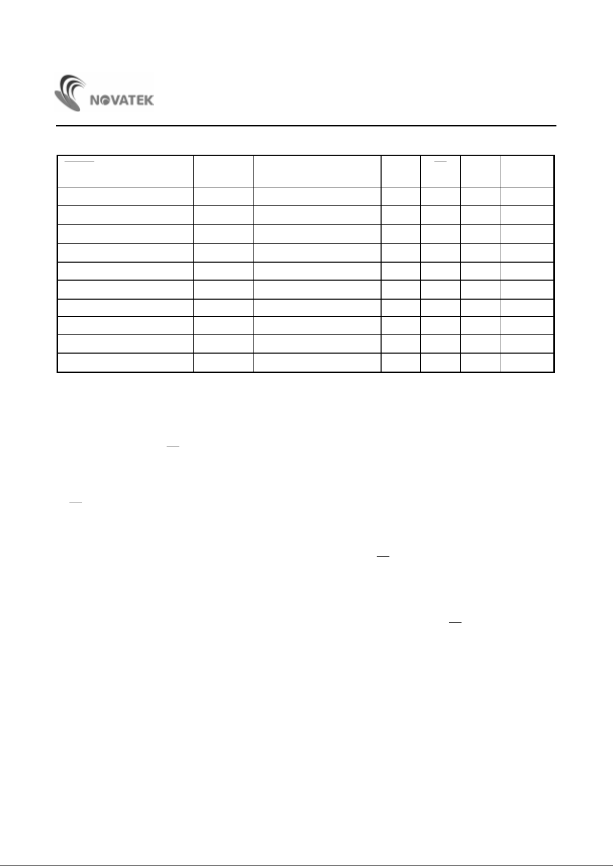
OTP ROM Mega Cell Timing Waveforms (PRO G RAM Mode)
A0 - A14
DB0 - DB7
CE
OE
PGM
VPP
MODE DEC.
TEST = VPP, MODE [0..2] = 000;
D IN
DOUT
Tms
Tmh
Tds
Tpw Tdh
Tdv
Tdf
Tvs
Tas
Tces
Tceh
Tah
NT68P61A
12
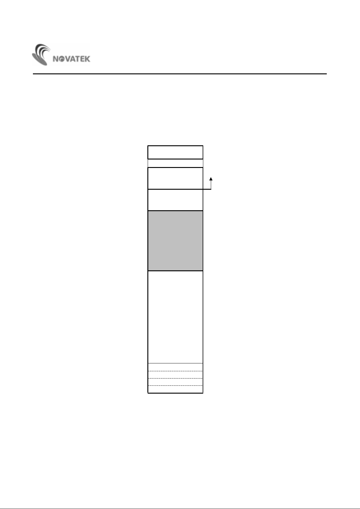
OTP ROM Mega cell Mode Selection
RESET
= 12.75V, OSCI = VIL,
P16 = V
IH
, DAC0 = V
IL
Mode [0..2] Mode CE
OE
VPP DB0 -
DB7
not VPP - - - Normal Operating - - - -
VPP 000 Output Disable -
V
IH
- high-Z
VPP 000 Program
V
IH
V
IH
VPP dat a i n
VPP 000 Program Verify
V
IH
V
IL
VPP data out
VPP 000 Program Inhibi t ( St andby)
V
IL
- VPP high-Z
VPP 001 Security (Program)
V
IH
- VPP data i n
VPP 010 Wo r d -line Stress - - VPP VPP 011 Bit- line Stress - - VPP "0"
VPP 100 OTP Row (after pkg)
V
IH
V
IH
VPP dat a i n
VPP 101 OTP Column (after pkg)
V
IH
V
IH
VPP dat a i n
* The security byte is at address $0000.
READ
NT68P61A's OTP ROM mega cell has 2 control pins. CE
(Chip Enable) controls the operation power and is used
for device selection. The
OE
(Output Enable) controls
the output buffers.
OUTPUT DISABLE
If
OE
= VIH, the outputs will be in a high impedance
state. Two or more ROMs can be connected together on
a comm on bus.
STANDBY
By applying a low power level to the CE input , the chip
enters STANDBY reducing the operating current to
100µA.
PROGRAM
Initially, all bits are in "1" state which is the erased state.
The program operation is to introduce "0" data int o the
desired bit locations by electrical programming. When
the VPP input is at 12.75V and CE is at V
IH
, the chip
enters the PROGRAMMING mode.
PROGRAM VERIFY
The VERIFY mode is to check if the desired data is
correctly programmed on the programmed bit. The
VERIFY is accomplished with CE at V
IH
, VPP input is at
12.75V, and
OE
= VIL.
PROGRAM INHIBIT
Using this mode, programming of two or more OTP
ROMs in parallel with dif ferent data is accomplished. All
inputs except for CE and
OE
may be commonly
connected, and a TTL high level program pulse is
applied to the CE of the desired device only and TTL
high level signal is appli ed to the other devices.
NT68P61A
13
4. RAM: 256 X 8 bits
256 X 8-bit SRAM is used f or dat a memory and stack. The RAM addressing range is f r om $0080 to $017F. From $0100 t o
$017F is used as the EDID data buffer when activating DDC1/2B mode transmission. The contents of RAM are
undetermined at power-up and are not affected by system reset. Software program mers can allocate stack area in t he
RAM by setting stack point er register S. Because the 6502 default stack pointer is $01FF, progr amm ers must set register
S to FFH when starting the program, so the stack area will map $01FF - $0180 to $00FF - $0080.
as; LDX #$FF
TXS
RAM
Unused
$0000
$0080
$0100
$00FF
$A000
$FFFF
stack pointer
$FFFE
$FFFD
$FFFC RST-L
RST-H
IRQ-L
IRQ-H
RESET vector
IRQ vector
$017F
EDID
$0180
(24K Bytes)
OTP
ROM
$0025
System Registers
Unused
$BFFF
NT68P61A
14
5. System Regist ers
Addr. Register INIT Bit7 Bit6 Bit5 Bit4 Bit3 Bit2 Bit1 Bit0
$0000 PT0 FFH P07 P06 P05 P04 P03 P02 P01 P00 RW
$0001 PT1 7FH - P16 P15 P14 P13 P12 P11 P10 RW
$0002 PT2DIR FFH
P27OE P26OE P25OE P24OE P23OE P22OE P21OE P20OE
W
$0003 PT2 FFH P27 P26 P25 P24 P23 P22 P21 P20 RW
$0004 PT3 03H - - - - - - P31 P30 RW
$0005 MD CON 07H
-
-
-
-
-
-
-
-
-
INSEN
-
HSEL
S/
C
S/
C
MD1/
2
MD1/
2
R
W
$0006 HV CON 2FH HCNTOV VCNTOV HSYNCI VSYNCI HPOLI VPOLI
HPOLO VPOLORW
$0007 HCNT L 00H HCL7 HCL6 HCL5 HCL4 HCL3 HCL2 HCL1 HCL0 R
$0008 HCNT H 00H - - - - HCH3 HCH2 HCH1 HCH0 R
$0009 VCNT L 00H VCL7 VCL6 VCL5 VCL4 VCL3 VCL2 VCL1 VCL0 R
$000A VCNT H 00H - - - - VCH3 VCH2 VCH1 VCH0 R
$000B SYNCON FFH
NOHALF
ENHALF
-
FRUN FRFREQ
HALFPOL
ENH ENV
W
$000C ENDAC FFH
ENAD1 ENAD0 ENDK13 ENDK12 ENDK11 ENDK10 ENDK9 ENDK8
W
$000D AD0 REG C0H
CEND
CSTA
AD05 AD04 AD03 AD02 AD01 AD00
R
W
$000E AD1 REG 00H - - AD15 AD14 AD13 AD12 AD11 AD10 R
$000F IEX 00H - - IEINTS IEINTD IEINTA IEINTR IEINTE IEINTV W
NT68P61A
15
System Registers (continu ed)
Addr. Register INIT Bit7 Bit6 Bit5 Bit4 Bit3 Bit2 Bit1 Bit0
$0010 IRQX 00H - - IRQINTS IRQINTD IRQINTA IRQINTR IRQINTE IRQINTV R
$0011 CLR FLG 00H CLRHOV CLRVOV CLRINTS CLRINTD CLRINTA CLRINTR CLRINTE CLRINTV W
$0012 CLR WDT - 01010101W
$0013 II ADR FFH AR7 AR6 AR5 AR4 AR3 AR2 AR1 - W
$0014 II DAT 00H SR7 SR6 SR5 SR4 SR3 SR2 SR1 SR0 RW
$0015 II STS 08H - - START
START
STOP
STOP
ENDDC
TRX
RXAK - R
W
$0016 BT 00H BT7 BT6 BT5 BT4 BT3 BT2 BT1 BT0 W
$0017 BT CON 03H ------TBS
ENBT
W
$0018 DACH0 80H DKVL7 DKVL6 DKVL5 DKVL4 DKVL3 DKVL2 DKVL1 DKVL0 RW
$0019 DACH1 80H DKVL7 DKVL6 DKVL5 DKVL4 DKVL3 DKVL2 DKVL1 DKVL0 RW
$001A DACH2 80H DKVL7 DKVL6 DKVL5 DKVL4 DKVL3 DKVL2 DKVL1 DKVL0 RW
$001B DACH3 80H DKVL7 DKVL6 DKVL5 DKVL4 DKVL3 DKVL2 DKVL1 DKVL0 RW
$001C DACH4 80H DKVL7 DKVL6 DKVL5 DKVL4 DKVL3 DKVL2 DKVL1 DKVL0 RW
$001D DACH5 80H DKVL7 DKVL6 DKVL5 DKVL4 DKVL3 DKVL2 DKVL1 DKVL0 RW
$001E DACH6 80H DKVL7 DKVL6 DKVL5 DKVL4 DKVL3 DKVL2 DKVL1 DKVL0 RW
$001F DACH7 80H DKVL7 DKVL6 DKVL5 DKVL4 DKVL3 DKVL2 DKVL1 DKVL0 RW
$0020 DACH8 80H DKVL7 DKVL6 DKVL5 DKVL4 DKVL3 DKVL2 DKVL1 DKVL0 RW
$0021 DACH9 80H DKVL7 DKVL6 DKVL5 DKVL4 DKVL3 DKVL2 DKVL1 DKVL0 RW
$0022 DACH10 80H DKVL7 DKVL6 DKVL5 DKVL4 DKVL3 DKVL2 DKVL1 DKVL0 RW
$0023 DACH11 80H DKVL7 DKVL6 DKVL5 DKVL4 DKVL3 DKVL2 DKVL1 DKVL0 RW
$0024 DACH12 80H DKVL7 DKVL6 DKVL5 DKVL4 DKVL3 DKVL2 DKVL1 DKVL0 RW
$0025 DACH13 80H DKVL7 DKVL6 DKVL5 DKVL4 DKVL3 DKVL2 DKVL1 DKVL0 RW
Note: The line above a writable signal name indicate an active low signal
The dash line in these control register indicate an undefined bit
The address of control register from $0026 t o $007F ar e not used.
 Loading...