

Page 1

PAMS Technical Documentation
RAE–2 Series PDA Phone
Chapter 4
UIF Module BS2
Original 02/99 Copyright 1999 Nokia Mobile Phones. All rights reserved.
Page 2
RAE–2
PAMS
UIF Module BS2
Amendment
Number
AMENDMENT RECORD SHEET
Date Inserted By Comments
02/99
Original
Technical Documentation
Page 4 – 2
Original 02/99
Page 3

PAMS
RAE–2
Technical Documentation
CONTENTS – User Interface
Introduction 4 – 4. . . . . . . . . . . . . . . . . . . . . . . . . . . . . . . . . . . . . . . . . . . .
Technical Summary 4 – 4. . . . . . . . . . . . . . . . . . . . . . . . . . . . . . . . . . . . .
Technical Specifications 4 – 5. . . . . . . . . . . . . . . . . . . . . . . . . . . . . . .
DC Characteristics 4 – 5. . . . . . . . . . . . . . . . . . . . . . . . . . . . . . . . .
AC Characteristics 4 – 6. . . . . . . . . . . . . . . . . . . . . . . . . . . . . . . . . . . .
Interface to BS1 PDA Module 4 – 6. . . . . . . . . . . . . . . . . . . . . . . . . .
Interface to BS8 CMT Module 4 – 10. . . . . . . . . . . . . . . . . . . . . . . . . .
Interface to BC2 LCD Module 4 – 10. . . . . . . . . . . . . . . . . . . . . . . . . .
Interface to PDA LCD Display 4 – 11. . . . . . . . . . . . . . . . . . . . . . . . .
Interconnection Diagram 4 – 14. . . . . . . . . . . . . . . . . . . . . . . . . . . . . .
Functional Description 4 – 14. . . . . . . . . . . . . . . . . . . . . . . . . . . . . . . . . . .
Power Distribution Diagram 4 – 14. . . . . . . . . . . . . . . . . . . . . . . . . . . .
CMT LCD Display Circuit 4 – 15. . . . . . . . . . . . . . . . . . . . . . . . . . . . . .
PDA LCD Display Circuit 4 – 16. . . . . . . . . . . . . . . . . . . . . . . . . .
Backlighting Circuit of CMT LCD And Keyboard 4 – 17. . . . . .
PDA LCD Backlighting Circuit 4 – 18. . . . . . . . . . . . . . . . . . . . .
PDA Function Keyboard And CMT Keyboard Circuit 4 – 19. .
UIF Module BS2
Page No
Original 02/99
Page 4 – 3
Page 4

RAE–2
PAMS
UIF Module BS2
Introduction
This document describes the RAE–2 UI module BS2. The module comprises PDA LCD display and function keys and all CMT UI electronics except the audio components.
Technical Summary
The following sections of circuitry are included in the BS2 UI module:
– External components of BC2 CMT LCD module
– External components of PDA LCD display
– Backlighting circuit of CMT LCD display and keyboard
– PDA display backlighting circuit
– PDA function keyboard and CMT keyboard switch matrices including
key dome sheets (3 pcs)
Technical Documentation
– RF coaxial cable connector and antenna clip
Other parts covered in this document:
– BC2 CMT LCD module
– PDA LCD display
– PDA LCD display EL backlighting panel
– CMT LCD display and keyboard EL backlighting panel
Page 4 – 4
Original 02/99
Page 5
PAMS
RAE–2
Technical Documentation
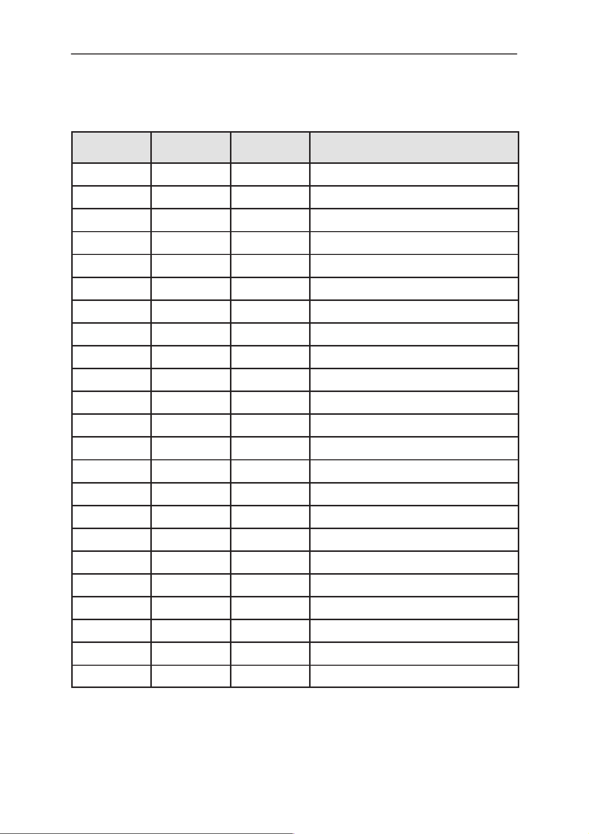
Technical Specifications
DC Characteristics
Pin /
Conn.
1/X700 VPDA Filtered
3/X700 VBB Regu-
Line Sym-
bol
Parame-
ter
battery
voltage
from PDA
lated
baseband
voltage
Minimum
3.0 3.6 4.1 V
13 30 mA PDA LCD back-
7 15 mA CMT LCD
2.7 2.8 2.85 V
UIF Module BS2
Typical /
Nominal
0 mA PDA and CMT
Maxi-
mum
300 A
Unit Notes
LCD backlights
OFF
light ON
backlight ON
42/X700 V17_i4 PDA LCD
intermediate
bias voltage
43/X700 V17_i3 PDA LCD
intermediate
bias voltage
44/X700 V17_i2 PDA LCD
intermediate
bias voltage
45/X700 V17_i1 PDA LCD
intermediate
bias voltage
47/X700 V17_OUT PDA LCD
bias voltage
1.3 1.5 1.7 V 1/13xV17_OUT
Throughout the
whole temperature range
1.4 1.5 1.6 V At +20°C
2.6 3.0 3.3 V 2/13xV17_OUT
Throughout the
whole temperature range
2.9 3.0 3.2 V At +20°C
13.5 16.4 18.6 V 11/13xV17_OU
T Throughout
the whole temperature range
15.4 16.4 17.4 V At +20°C
14.7 17.9 20.3 V 12/13xV17_OU
T Throughout
the whole temperature range
16.8 17.9 19.0 V At +20°C
16.0 19.4 22.0 V Throughout the
whole temperature range
Original 02/99
18.2 19.4 20.6 V At +20°C
Page 4 – 5
Page 6
RAE–2
g
tween in and
tween in and
baseband volt
PAMS
UIF Module BS2
Pin /
Conn.
49/X700 V28_1 PDA LCD
5,7,9,31,
34,36,38,
41,46,51/
X700
Line Sym-
bol
GND 0 V
Parame-
ter
logic supply voltage
AC Characteristics
Pin /
Conn.
6,7/
N700
Parameter Minimum Typical /
Frequency 152 158 165 Hz
Peak–to–peak volt-
age
RMS voltage 58 63 70 V
155 164 175 V
Technical Documentation
Minimum
2.7 2.8 2.85 V
Typical /
Nominal
0.3 2.0 mA
Nominal
mum
Maximum Unit Notes
NotesUnitMaxi-
Differential measurement between
the pins, NOT be-
p
ground
6,7/
N730
X790,
X791
Frequency 148 156 168 Hz
Peak–to–peak volt-
age
RMS voltage 61 65 70 V
Transmitter fre-
quency
Receiver frequency 935 960 MHz
160 164 170 V
890 915 MHz
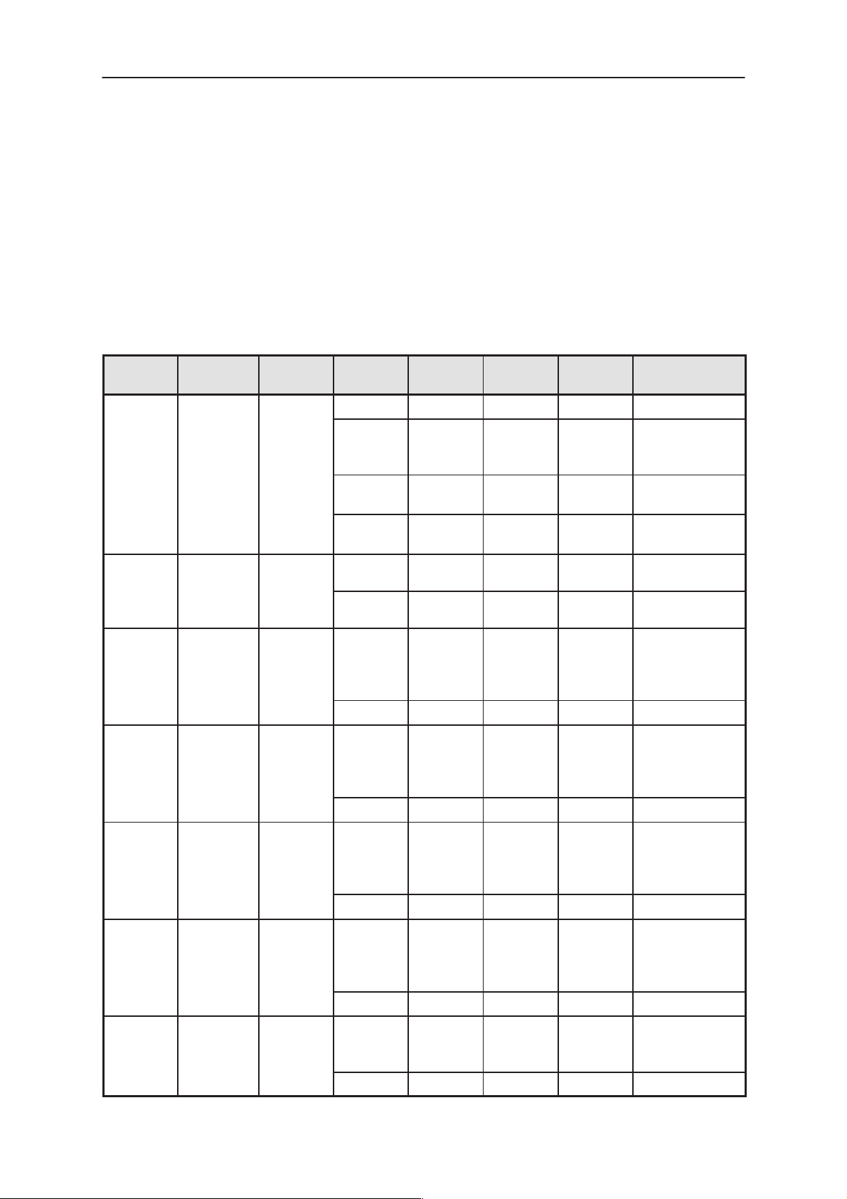
Interface to BS1 PDA Module
Pin I/O Line Symbol Parameter Mini-
mum
1 VPDA Filtered bat-
tery voltage
from PDA
2 O PWRKEYx Power on key 0
3 VBB Regulated
age
3.0 3.6 4.1 V
13 30 mA PDA LCD
7 15 mA CMT LCD
0.7xVBB
2.7 2.8 2.85 V
-
Differential measurement between
the pins, NOT be-
p
ground
Typical /
Nominal
0 mA PDA and CMT
Maxi-
mum
0.3xVBB
VBB
300 A
Unit Notes
V Low, Power
backlights
OFF
backlight ON
backlight ON
key pressed
High
Page 4 – 6
Original 02/99
Page 7

PAMS
RAE–2
Technical Documentation
ParameterLine SymbolI/OPin
4 I LCDRSTx CMT LCD
driver reset
5 GND 0 V
6 I GENSDIO CMT LCD
driver serial
data
7 GND 0 V
8 I GENSCLK CMT LCD
driver bus
clock
9 GND 0 V
10 I LCDSCx CMT LCD
driver chip select
Minimum
0
0.7xVBB
0
0.7xVBB
0 4.0 MHz
0
0.7xVBB
0 3.2 4.0 MHz
0
0.7xVBB
Typical /
Nominal
mum
0.3xVBB
VBB
0.3xVBB
VBB
0.3xVBB
VBB
0.3xVBB
VBB
UIF Module BS2
NotesUnitMaxi-
V Low, Reset
active
High, Reset inactive
V Low
High
V Low
High
V Low, Chip se-
lected
High, Chip unselected
11 I LCDCD CMT LCD
driver command/data
selection
12 I APP_COL0 PDA function
keyboard column 0
13 I APP_COL1 PDA function
keyboard column 1
14 I APP_COL2 PDA function
keyboard column 2
15 I APP_COL3 PDA function
keyboard column 3
16 O APP_ROW0 PDA function
keyboard row
0
17 O APP_ROW1 PDA function
keyboard row
1
0
0.7xVBB
0
0.7xVSY
S
0
0.7xVSY
S
0
0.7xVSY
S
0
0.7xVSY
S
0
0.7xVSY
S
0
0.7xVSY
S
0.3xVBB
VBB
0.3xVSY
S
VSYS
0.3xVSY
S
VSYS
0.3xVSY
S
VSYS
0.3xVSY
S
VSYS
0.3xVSY
S
VSYS
0.3xVSY
S
VSYS
V Low, Com-
mand
High, Data
V Low
High
V Low
High
V Low
High
V Low
High
V Low
High
V Low
High
18 I COL0 CMT Key-
board column
0
19 I COL1 CMT Key-
board column
1
Original 02/99
0
0.7xVBB
0
0.7xVBB
0.3xVBB
VBB
0.3xVBB
VBB
V Low
High
V Low
High
Page 4 – 7
Page 8

RAE–2
PAMS
UIF Module BS2
ParameterLine SymbolI/OPin
20 I COL2 CMT Key-
board column
2
21 I COL3 CMT Key-
board column
3
22 I COL4 CMT keyboard
column 4
23 O ROW0 CMT keyboard
row 0
24 O ROW1 CMT keyboard
row 1
25 O ROW2 CMT keyboard
row 2
26 O ROW3 CMT keyboard
row 3
27 I CMT_BL_ON CMT LCD and
keyboard
backlight enable
Minimum
0
0.7xVBB
0
0.7xVBB
0
0.7xVBB
0
0.7xVBB
0
0.7xVBB
0
0.7xVBB
0
0.7xVBB
0
0.7xVBB
Typical /
Nominal
Technical Documentation
NotesUnitMaxi-
mum
0.3xVBB
VBB
0.3xVBB
VBB
0.3xVBB
VBB
0.3xVBB
VBB
0.3xVBB
VBB
0.3xVBB
VBB
0.3xVBB
VBB
0.3xVBb
VBB
V Low
High
V Low
High
V Low
High
V Low
High
V Low
High
V Low
High
V Low
High
V Low, backlight
OFF
High, backlight
ON
28 I PDA_BL_ON PDA LCD
backlight enable
29 I LCDD3 PDA LCD
data, leftmost
pixel
30 I LCDD2 PDA LCD data 0
31 GND 0 V
32 I LCDD1 PDA LCD data 0
33 I LCDD0 PDA LCD
data, right-
most pixel
34 GND 0 V
35 I SCK PDA LCD bus
clock
0
0.7xVSY
S
0
0.8xVSY
S
0.8xVSY
S
0.8xVSY
S
0
0.8xVSY
S
0
0.8xVSY
S
0 2.3 3.2 MHz
0.3xVSY
S
VSYS
0.2xVSY
S
VSYS
0.2xVSY
S
VSYS
0.2xVSY
S
VSYS
0.2xVSY
S
VSYS
0.2xVSY
S
VSYS
V Low, backlight
OFF
High, backlight
ON
V Low
High
V Low
High
V Low
High
V Low
High
V Low
High
36 GND GND 0 V
Page 4 – 8
Original 02/99
Page 9

PAMS
RAE–2
Technical Documentation
ParameterLine SymbolI/OPin
37 I LC PDA LCD line
pulse
38 GND 0 V
39 I M PDA LCD AC
modulation
40 I FRM PDA LCD
frame pulse
Minimum
0
0.8xVSY
S
0 13.6 20 kHz
0
0.8xVSY
S
0 1 kHz
0
0.8xVSY
S
0 67 100 Hz
Typical /
Nominal
870 ns Pulse ’high’
mum
0.2xVSY
S
VSYS
0.2xVSY
S
VSYS
0.2xVSY
S
VSYS
UIF Module BS2
NotesUnitMaxi-
V Low
High
time
V Low
High
V Low
High
75 s Pulse ’high’
41 GND 0 V
42 V17_i4 PDA LCD in-
termediate
bias voltage
43 V17_i3 PDA LCD in-
termediate
bias voltage
44 V17_i2 PDA LCD in-
termediate
bias voltage
45 V17_i1 PDA LCD in-
termediate
bias voltage
1.3 1.5 1.7 V 1/13xV17_OU
1.4 1.5 1.6 V At +20°C
2.6 3.0 3.3 V 2/13xV17_OU
2.9 3.0 3.2 V At +20°C
14.4 16.4 18.3 V 11/13xV17_O
16.1 16.8 17.4 V At +20°C
15.8 17.9 19.9 V 12/13xV17_O
time
T Throughout
the whole temperature range
T Throughout
the whole temperature range
UT Throughout the whole
temperature
range
UT Throughout the whole
temperature
range
17.5 18.3 19.0 V At +20°C
46 GND 0 V
47 V17_OUT PDA LCD bias
voltage
17.1 19.8 21.6 V Throughout
19.0 19.8 20.6 V At +20°C
Original 02/99
the whole temperature range
Page 4 – 9
Page 10

RAE–2
ic su ly volt
PAMS
UIF Module BS2
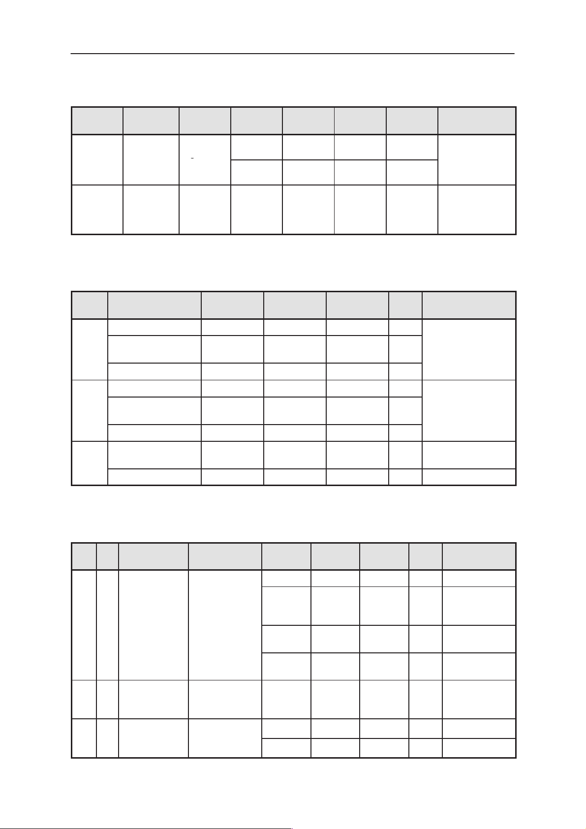
ParameterLine SymbolI/OPin
48 I LCD_ON PDA LCD en-
able
49 V28_1 PDA LCD log-
pp
age
50 O LCD_TEMP PDA LCD
temperature
51 GND 0 V
Note: VSYS is PDA system voltage used in BS1 module, min. 2.75 V, typ. 2.80 V, max. 2.85
V.
Minimum
0
0.8xVSY
S
2.7 2.8 2.85 V
-
0.2 0.9 2.5 V Voltage range
0.88 0.90 0.91 V At +25°C
Typical /
Nominal
0.3 2.0 mA
Technical Documentation
mum
0.2xVSY
S
VSYS
NotesUnitMaxi-
V Low
High
throughout the
whole temperature range
Interface to BS8 CMT Module
Conn. Parameter Mini-
mum
X790,
X791
Impedance 50 W
Transmitter frequency 890 915 MHz
Receiver frequency 935 960 MHz
Max. output power 2W (33 dBm)
Typical / Nomi-
nal
Maxi-
mum
Unit /
Notes
Notes
Interface to BC2 LCD Module
Pin Line Symbol Parameter Mini-
mum
1 VBB Supply voltage 2.7 2.8 2.85 V
2 GENSCLK Serial clock input 0 3.2 4.0 MHz
0 0.3xVBB V Low
0.7xVBB VBB V High
3 GENSDIO Serial data input 0 0.3xVBB Low
T ypical Maxi-
mum
300 mA
Unit Notes
0.7xVBB VBB High
4 LCDCD Control/display data
flag input
5 LCDCSx Chip select input 0 0.3xVBB Low, Chip se-
Page 4 – 10
0 0.3xVBB Low, Control
0.7xVBB VBB High, Data
lected
0.7xVBB VBB High, Chip
unselected
Original 02/99
Page 11

PAMS
RAE–2
Technical Documentation
ParameterLine SymbolPin
mum
6 OSC* External clock for LCD 30.4 32.0 33.6 kHz Connected to
7 GND Ground 0 V
8 VOUT DC/DC voltage con-
verter output
9 LCDRSTx Reset 0 0.3xVBB Low, Reset
0.7xVBB VBB High,Reset
* External oscillator is not used in BS2.
TypicalMini-
mum
6.8 9
UIF Module BS2
NotesUnitMaxi-
VBB on UI
Active
Inactive
Connection layout diagram of interface to BC2 module
9
Display
Driver
1
Viewing through LCD cell
Interface to PDA LCD Display
Table 1. Interface to PDA LCD display, connector X730.
Pin Line Symbol Parameter Minimum Typical /
Nominal
12V17_OUT PDA LCD bias
voltage
16.0 19.4 22.0 V Throughout the
18.2 19.4 20.6 V At +20°C
IC
Maxi-
mum
Unit Notes
whole temperature range
3 V17_i1 PDA LCD inter-
mediate bias
voltage
Original 02/99
14.7 17.9 20.3 V 12/13xV17_OU
T Throughout
the whole temperature range
16.8 17.9 19.0 V At +20°C
Page 4 – 11
Page 12
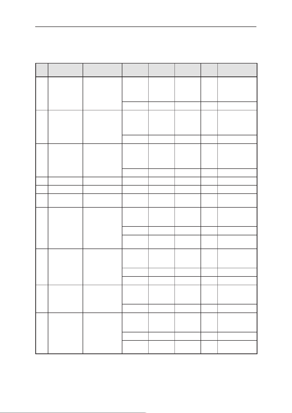
RAE–2
PAMS
UIF Module BS2
Table 1. Interface to PDA LCD display, connector X730. (continued)
4 V17_i2 PDA LCD inter-
mediate bias
voltage
5 V17_i3 PDA LCD inter-
mediate bias
voltage
6 V17_i4 PDA LCD inter-
mediate bias
voltage
Technical Documentation
MinimumParameterLine SymbolPin
13.5 16.4 18.6 V 11/13xV17_OU
15.4 16.4 17.4 V At +20°C
2.6 3.0 3.3 V 2/13xV17_OUT
2.9 3.0 3.2 V At +20°C
1.3 1.5 1.7 V 1/13xV17_OUT
1.4 1.5 1.6 V At +20°C
Typical /
Nominal
mum
NotesUnitMaxi-
T Throughout
the whole temperature range
Throughout the
whole temperature range
Throughout the
whole temperature range
7 GND 0 V
8 GND 0 V
9 V28_1 2.7 2.8 2.85 V PDA LCD logic
supply voltage
10 FRM PDA LCD frame
pulse
11 SCK PDA LCD bus
clock
12 M PDA LCD AC
modulation
13 LC PDA LCD line
pulse
0
0.8xVSY
S
70 100 Hz
75 s Pulse ’high’
0
0.8xVSY
S
0 2.3 3.2 MHz
0
0.8xVSY
S
0 2.5 3.4 kHz
0
0.8xVSY
S
0.2xVSY
S
VSYS
0.2xVSY
S
VSYS
0.2xVSY
S
VSYS
0.2xVSY
S
VSYS
V Low
High
time
V Low
High
V Low
High
V Low
High
Page 4 – 12
0 32 44.5 kHz
870 ns Pulse ’high’
time
Original 02/99
Page 13

PAMS
RAE–2
Technical Documentation
Table 1. Interface to PDA LCD display, connector X730. (continued)
14 LCD_ON PDA LCD en-
able
15 LCDD3 PDA LCD data,
leftmost pixel
16 LCDD2 PDA LCD data 0
17 LCDD1 PDA LCD data 0
18 LCDD0 PDA LCD data,
rightmost pixel00.8xVSY
MinimumParameterLine SymbolPin
0
0.8xVSY
S
0
0.8xVSY
S
0.8xVSY
S
0.8xVSY
S
S
Typical /
Nominal
mum
0.2xVSY
S
VSYS
0.2xVSY
S
VSYS
0.2xVSY
S
VSYS
0.2xVSY
S
VSYS
0.2xVSY
S
VSYS
UIF Module BS2
NotesUnitMaxi-
V Low, Display
OFF
High, Display
ON
V Low
High
V Low
High
V Low
High
V Low
High
Note: VSYS is PDA system voltage used in BS1 module, min. 2.75 V, typ. 2.80 V, max. 2.85
V.
Signal number 1 is marked with a triangle in the connector X730.
Original 02/99
Page 4 – 13
Page 14

RAE–2
PAMS
UIF Module BS2
Interconnection Diagram
BC2 CMT
LCD Module
BS2
Hinge Flex
BS1
CMT Keyboard and
Display Backlight
5106 10
PDA Function
Keyboard
BoBo Connector
Technical Documentation
PDA Display
Backlight
Scotty
DisplayCMT Keyboard
PDA LCD
MAD
BS8
Functional Description
Power Distribution Diagram
V28_1
V17_OUT
V17_i1
V17_i2
V17_i3
V17_i4
VPDA
VBB
CMT LCD CMT LCD
Backlight
Driver
CMT EL
Panel
PDA LCD
Backlight
Driver
PDA EL
Panel
Coaxial Cable
PDA LCD
Page 4 – 14
GND
Original 02/99
Page 15

PAMS
RAE–2
Technical Documentation
CMT LCD Display Circuit
The display circuit includes the LCD module BC2 and two capacitors. The
LCD module uses COG (Chip On Glass) technology. The connection
method for chip on the glass is ACF, Adhesive Conductive Film. The LCD
module is electrically connected to UI board with gold wired elastomer.
Two external capacitors are placed on UI PCB.
The display driver includes hw–reset, voltage tripler or quadrupler which
depends on temperature, temperature compensating circuit and low power control. The driver includes a 84x48 RAM memory which is used for
storing display data. The driver does not include character generator
ROM. One bit in RAM is mapped directly to one pixel on display.
Main characteristics of the CMT LCD display:
– Display resolution: 84 x 48
– Viewing area: 34.96 x 23.50 mm
– Dot size: 0.31 x 0.37 mm
– Dot pitch: 0.345 x 0.405 mm
– Display type: Transflective black and white FSTN
UIF Module BS2
Original 02/99
Page 4 – 15
Page 16

RAE–2
PAMS
UIF Module BS2
PDA LCD Display Circuit
The PDA LCD display circuit consists of the LCD display 4850049, logic
and bias voltage filtering capacitors and an NTC resistor that is used to
measure the temperature of the display. The voltage over the NTC is
read by PDA SW via Phaser power supply ASIC and the information is
used for contrast control of the display.
Main characteristics of the PDA LCD display:
– Display resolution: 640 x 200
– Viewing area: 111.8 x 37.0 mm
– Dot size: 0.16 x 0.16 mm
– Dot pitch: 0.17 x 0.17 mm
– Display type: Transflective black and white FSTN
The PDA LCD interface is a typical black–and–white LCD interface with
four data bits, pixel clock, line and frame pulse signals, AC modulation
signal and enable signal. Logic and bias voltages are supplied by the
Phaser power supply ASIC located in the PDA module.
Technical Documentation
Page 4 – 16
Original 02/99
Page 17

PAMS
RAE–2
Technical Documentation
Backlighting Circuit of CMT LCD And Keyboard
An electroluminescent (EL) panel is used for CMT LCD and keyboard
backlighting. Electrically it can be considered as a capacitor. An inverter
circuit is used to generate the high voltage AC to drive the EL panel. The
inverter can be divided into two sections: power converter section and
lamp driver section.
The power converter section employs a switch–mode converter to generate a voltage of maximum 90V. This voltage is connected to the EL panel
through the lamp driver section, which changes the polarity of the output
pins at a frequency that is set by one external resistor. Since the switch–
mode converter’s output is regulated to 90 volts at maximum, it is possible to achieve almost constant illuminance from the EL panel throughout
the battery voltage range.
Connection between the EL panel and the PCB is a simple pressure contact. The frame of the CMT display module has two springs that press
the EL panel against the pads on the PCB.
UIF Module BS2
NOTE: The EL driver output voltage between pins 6 and 7 is over 150 V
peak–to–peak. When making measurements, be sure that measuring
equipment like oscilloscope, probe etc. have high enough voltage rating.
There is no risk of getting a harmful or fatal electric shock due to low current driving capability of the inverter.
Table 2. CMT display illuminance measured with Tektronics J17 on the surface of the dis-
play lense.
Parameter Minimum Typical /
Display illuminance
1.5 2.1 cd/m2Throughout the
1.6 1.8 2.0 cd/m2VPDA = 3.5 V
Nominal
Maximum Unit Notes
VPDA voltage range
Original 02/99
Page 4 – 17
Page 18

RAE–2
PAMS
UIF Module BS2
Technical Documentation
PDA LCD Backlighting Circuit
Electroluminescent (EL) panel is used for PDA LCD backlighting. The circuit is similar to the CMT keyboard and the display backlighting circuit,
only some component values are different.
PDA display frame presses the EL panel contacts against the pads on
PCB.
NOTE: The EL driver output voltage between pins 6 and 7 is over 150 V
peak–to–peak. When making measurements, be sure that measuring
equipment like oscilloscope, probe etc. have high enough voltage rating.
There is no risk of getting a harmful or fatal electric shock due to low current driving capability of the inverter.
Table 3. PDA display illuminance measured with Tektronics J17 on the surface of the dis-
play.
Parameter Minimum Typical /
Display illuminance
1.0 2.0 cd/m2Throughout the
1.2 1.5 1.8 cd/m2VPDA = 3.5 V
Nominal
Maximum Unit Notes
VPDA voltage range
Page 4 – 18
Original 02/99
Page 19

PAMS
RAE–2
Technical Documentation
PDA Function Keyboard And CMT Keyboard Circuit
There are 5 columns and 4 rows in the CMT keyboard matrix and 2 rows
and 4 columns in the PDA function keyboard matrix. The power key is
connected to the CMT row 0 through a diode, that prevents the POWERKEYx line from being pulled down when the other keys are scanned. A
normal keyboard scanning is used to read both matrices.
UIF Module BS2
Original 02/99
Page 4 – 19
Page 20

RAE–2
PAMS
UIF Module BS2
Technical Documentation
This page intentionally left blank.
Page 4 – 20
Original 02/99
 Loading...