

Page 1

PAMS Technical Documentation
HFU–2
Original 11/97
Page 2

PAMS
HFU–2
Technical Documentation
CONTENTS
Introduction 3. . . . . . . . . . . . . . . . . . . . . . . . . . . . . . . . . . . . . . . . . . . .
Technical Summary 3. . . . . . . . . . . . . . . . . . . . . . . . . . . . . . . . . . .
List of Modules 4. . . . . . . . . . . . . . . . . . . . . . . . . . . . . . . . . . . . . . .
Operation 4. . . . . . . . . . . . . . . . . . . . . . . . . . . . . . . . . . . . . . . . . . .
Supply Voltage and Power Consumption 4. . . . . . . . . . . . . . . .
Charging voltage limits within current specifications fulfilled 5
Audio Specifications, electrical 5. . . . . . . . . . . . . . . . . . . . . . . . .
HFS–12 Audio Specifications, acoustic 6. . . . . . . . . . . . . . . . . .
HFM–8 Audio Specifications, acoustic 6. . . . . . . . . . . . . . . . . . .
Audio signal levels 6. . . . . . . . . . . . . . . . . . . . . . . . . . . . . . . . . . . .
Signals and Connections 6. . . . . . . . . . . . . . . . . . . . . . . . . . . . . .
Block Diagram 7. . . . . . . . . . . . . . . . . . . . . . . . . . . . . . . . . . . . . . .
Exploded View of HFU–2 8. . . . . . . . . . . . . . . . . . . . . . . . . . . . . .
Parts list of ED2 (EDMS Issue )
Code: 0200948 9. . . . . . . . . . . . . . . . . . . . . . . . . . . . . . . . . . . . . . . . .
Page 2
Original 11/97
Page 3
PAMS
Technical Documentation
Introduction
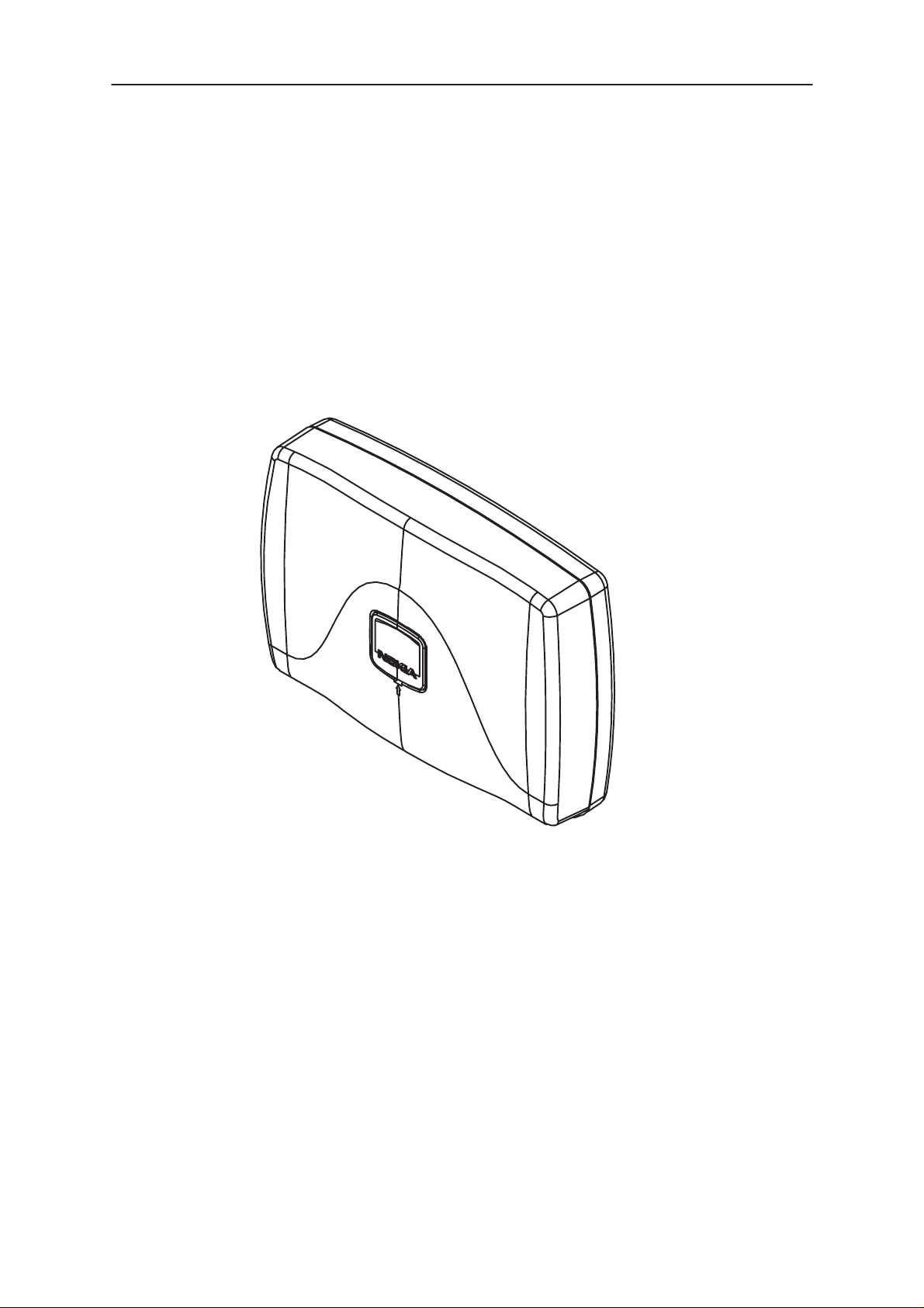
The HFU–2 is a handsfree unit for DCT3 compatible handportable
phones. It provides rapid charging for the phone, a possibility to use HF–
operation and connections to the data–card and handset unit. The HF
box can be connected directly to the Mobile holder MCC–1 via the external cable.
HFU–2
Technical Summary
The HFU–2 has connections to car battery, car ignition sense, car radio
muting, antenna motor control, data–card, handset HSU–1, external
speaker and microphone. The unit has a System–connector that provides an interface to the Mobile holder MCC–1 via the external cable.
The unit consists of a rapid charger, HF–microphone– and speaker amplifiers, interface to handset, – datacard and –phone, voltage regulators and
control circuit (microprocessor).
The HFU–2 is always connected to the car battery. To save the car battery, HFU–2 goes in to the sleep mode if the car is not running and/or the
phone is not connected.
Original 11/97
Page 3
Page 4
PAMS
HFU–2
Technical Documentation
List of Modules
Name of module Type code Material
code
HF unit HFU–2 0694049 Advanced handsfree unit
HF module ED2 0200948 ED2 Advanced hadsfree module
Assembly parts MHFU–2 0261602 Mechanical Parts
Notes
Operation
Phone not connected (sleep mode):
When the phone is not connected the current consumption of
the device has been minimized. The switching mode power
supply (SMPS) and audio circuits has been turned off. HFU–2
is only waiting a phone to be connected.
Phone connected (active mode):
When the phone is connected to the HFU–2 it goes into the active mode. In the active mode the device provides charging
current to the phone. It also can provide hands free call option
using the external speaker and the external microphone or
micspeaker unit. If more private call wants to be made, the
phone itself can be used as a handset without losing the external antenna connection or with handset (option).
The phone controls all functions of HFU–2. In the active mode
the HFU–2 sends all state transitions to phone via mbus.
HFU–2 also provides car radio mute function during call.
HFU–2 can control the mobile antenna motor if it is installed to
the car.
Supply Voltage and Power Consumption
Conn. / pin Line Symbol Minimum Typical /
Nominal
X300 / 6 GND 0 VDC
Maximum Unit / Notes
X300 / 1 VB 8.0 16 VDC (working)
X300 / 1 VB 10.8 13.5 16 VDC (spec. fulfill)
X300 / 1 VB 0.05 1 2 IDC/A (operating)
X300 / 1 VB 0.2 0.8 1 IDC/mA (sleep
mode)
Page 4
Original 11/97
Page 5
PAMS
Technical Documentation
HFU–2
Charging voltage limits within current specifications fulfilled
Conn. / pin Line Symbol Minimum Typical /
Nominal
X200 / 7 GND 0 0 0.1 VDC
X200 / 2 +10VA 9.50 10.0 10.55 VDC
X200 / 2 +10VA 11 200 IDC / mA
Conn. / pin Line Symbol Minimum Typical /
Nominal
X100 /
5,6,11
X100 / 8,9 V_IN 3 8.5 VDC
X100 / 12 VB 8 16 VDC / car battery
X100 / 12 VB 500 IDC / mA
GND 0 0 0.1 VDC
Maximum Unit / Notes
Maximum Unit / Notes
Audio Specifications, electrical
Minimum Typical /
Nominal
Max speaker output power at
distortion=1%, 1 kHz sine
HF–speaker amplifier gain 27 29 31 dB
PSRR, XEAR line –60 –68 dB
CMRR, XEAR–SGND to
speaker
HF–mic amplifier gain 27 30 33 dB
Mic level at XMIC–SGND,
(clipping level)
Mic distortion at XMIC–
SGND, at Vo = 100 mVrms,
1 kHz
Noise voltage, HFMIC 5 uVrms psofometric
PSRR, XMIC –60 –67 dB
Crosstalk XEAR–SGND to
XMIC
3.0 3.1 W / Rload = 8 ohm
–50 –55 dB
2000 2800 mVpp
0.15 0.4 %
– 55 – 45 dB / electrical, 1kHz
Maximum Unit / Notes
Original 11/97
Page 5
Page 6

PAMS
HFU–2
Technical Documentation
HFS–12 Audio Specifications, acoustic
Minimum Typical /
Nominal
Electroacoustic transfer function (RX) dBPa/1V/0.5m
Speaker distortion level at
XEAR–SGND, d=5%
HF–speaker: SPL, approximate over 500 ... 3000 Hz
Equivalent input noise,
XEAR
Total noise, HF speaker 200 400 uVrms psofometric
11 15 19 dBPa / 1V at system
354 mVrms
87
–4
89
–2
Maximum Unit / Notes
connector is theoretical level
91
0
10 uVrms psofometric
dB / 1W / 1m
dBPa / 0.5W at 0,5m
HFM–8 Audio Specifications, acoustic
Minimum Typical /
Nominal
Electroacoustic transfer function (TX) dBV/dBPa/0.5m
Total noise, XMIC–SGND 140 300 uVrms psofometric
–28 –24 –20 dBV/–5dBPa/0.5m
Maximum Unit / Notes
Audio signal levels
Signal name / conn. / pin Minimum Typical /
Nominal
XEAR / X100 / 4 80 354 mVrms
SGND / X100 / 3 0 mVrms
XMIC / X100 / 2 60 990 mVrms
HFMIC / X400 / 2 2.0 mVrms
SPEAKER / X500 / 1 & 2 0.75 5 V rms
Maximum Unit / Notes
Signals and Connections
Connector Name Code Notes Specifications / Ratings
System connector X100 Charge, Mbus, Fbus, audio
lines, VB
Handset / Data connector X200 Mbus, Fbus, Handset au-
dio– lines, Hshook, 10V
Car connector X300 +VB, –VB, ign. sense, car
radio mute, antenna motor
control
HFMIC connector X400 External microphone 2.5 mm jack
EXT. SPEAKER connector X500 External speaker 3.2 mm jack
Modular 15 pin.
Modular 10 pin.
2 X 3 Power conn.
Page 6
Original 11/97
Page 7

PAMS
Technical Documentation
Block Diagram
CHARGE
SMPS
V_IN
CHRG_CTRL
EXTERNAL
I / O
CRM
CHGON
MBUS
IGNS
AMC
CONTROL
CIRCUITS
CRM
AMC
IGNS
protec–
tion
RESET
PWRON
HFU–2
VCC
DC connector
X300
VCC
POWER
SUPPLY
System connector X100
FBUS
HS / Data con–
nector X200
protec–
tion
protec–
tion
AUDIO
AUDIO
AUDIO
INTERFACE
EAR
POWER
AMPLIFIER
MUTE
MUTE
EAR
MUTE
LOGIC
protec–
tion
protec–
tion
MICROPHONE
AMPLIFIER
PASSIVE
MIC
External Microphone
Connector X200
External Speaker
Connector X500
Original 11/97
Page 7
Page 8

PAMS
HFU–2
Exploded View of HFU–2
Technical Documentation
5
4
Page 8
3
2
1
Original 11/97
Page 9

PAMS
Technical Documentation
HFU–2
Parts list of ED2 (EDMS Issue 5.1) Code: 0200948
ITEM CODE DESCRIPTION VALUE TYPE
R200 1415960 Melf resistor 33.2 k 1 % 0.2 W 0204
R201 1412409 Chip resistor 1.5 k 5 % 0.1 W 0805
R202 1430051 Chip resistor 4.7 k 5 % 0.063 W 0603
R203 1413829 Chip resistor 10 5 % 0.1 W 0805
R204 1413829 Chip resistor 10 5 % 0.1 W 0805
R205 1419007 Chip resistor 0.22 2 % 1210
R206 1413635 Chip resistor 100 k 5 % 0.1 W 0805
R207 1416393 Melf resistor 221 k 1 % 0.2 W 0204
R209 1430001 Chip resistor 100 5 % 0.063 W 0603
R210 1415791 Melf resistor 100 1 % 0.2 W 0204
R211 1413716 Chip resistor 220 k 5 % 0.1 W 0805
R212 1416273 Melf resistor 150 k 1 % 0.2 W 0204
R213 1430065 Chip resistor 10 k 5 % 0.063 W 0603
R214 1430089 Chip resistor 120 k 5 % 0.063 W 0603
R215 1430105 Chip resistor 560 k 5 % 0.063 W 0603
R216 1415664 Melf resistor 27.4 k 1 % 0.2 W 0204
R218 1412328 Chip resistor 820 5 % 0.1 W 0805
R219 1416798 Melf resistor 681 1 % 0.2 W 0204
R222 1410003 Chip resistor 33 k 1 % 0.1 W 0805
R223 1410001 Chip resistor 22 k 1 % 0.1 W 0805
R224 1414283 Chip resistor 100 k 1 % 0.1 W 0805
R225 1414283 Chip resistor 100 k 1 % 0.1 W 0805
R226 1413716 Chip resistor 220 k 5 % 0.1 W 0805
R227 1430051 Chip resistor 4.7 k 5 % 0.063 W 0603
R228 1430087 Chip resistor 100 k 5 % 0.063 W 0603
R233 1430015 Chip resistor 470 5 % 0.063 W 0603
R240 1430001 Chip resistor 100 5 % 0.063 W 0603
R245 1415960 Melf resistor 33.2 k 1 % 0.2 W 0204
R246 1414406 Chip resistor 5.6 k 5 % 0.1 W 0805
R270 1430087 Chip resistor 100 k 5 % 0.063 W 0603
R300 1430071 Chip resistor 22 k 5 % 0.063 W 0603
R301 1430087 Chip resistor 100 k 5 % 0.063 W 0603
R302 1430087 Chip resistor 100 k 5 % 0.063 W 0603
R303 1430071 Chip resistor 22 k 5 % 0.063 W 0603
R304 1412409 Chip resistor 1.5 k 5 % 0.1 W 0805
R306 1430071 Chip resistor 22 k 5 % 0.063 W 0603
R307 1430087 Chip resistor 100 k 5 % 0.063 W 0603
R310 1412261 Chip resistor 100 5 % 0.1 W 0805
R311 1430073 Chip resistor 27 k 5 % 0.063 W 0603
R312 1430073 Chip resistor 27 k 5 % 0.063 W 0603
R313 1430065 Chip resistor 10 k 5 % 0.063 W 0603
R315 1430065 Chip resistor 10 k 5 % 0.063 W 0603
R316 1430051 Chip resistor 4.7 k 5 % 0.063 W 0603
Original 11/97
Page 9
Page 10

PAMS
HFU–2
R317 1430087 Chip resistor 100 k 5 % 0.063 W 0603
R319 1430079 Chip resistor 47 k 5 % 0.063 W 0603
R321 1430071 Chip resistor 22 k 5 % 0.063 W 0603
R323 1414536 Chip resistor 200 k 1 % 0.1 W 0805
R324 1410003 Chip resistor 33 k 1 % 0.1 W 0805
R325 1430035 Chip resistor 1.0 k 5 % 0.063 W 0603
R327 1414536 Chip resistor 200 k 1 % 0.1 W 0805
R328 1410003 Chip resistor 33 k 1 % 0.1 W 0805
R331 1430065 Chip resistor 10 k 5 % 0.063 W 0603
R332 1430055 Chip resistor 6.8 k 5 % 0.063 W 0603
R333 1430055 Chip resistor 6.8 k 5 % 0.063 W 0603
R334 1414536 Chip resistor 200 k 1 % 0.1 W 0805
R335 1410003 Chip resistor 33 k 1 % 0.1 W 0805
R336 1430095 Chip resistor 220 k 5 % 0.063 W 0603
R337 1430095 Chip resistor 220 k 5 % 0.063 W 0603
R350 1430035 Chip resistor 1.0 k 5 % 0.063 W 0603
R351 1430065 Chip resistor 10 k 5 % 0.063 W 0603
R352 1430047 Chip resistor 3.3 k 5 % 0.063 W 0603
R353 1430065 Chip resistor 10 k 5 % 0.063 W 0603
R380 1430095 Chip resistor 220 k 5 % 0.063 W 0603
R400 1430043 Chip resistor 2.2 k 5 % 0.063 W 0603
R402 1430073 Chip resistor 27 k 5 % 0.063 W 0603
R403 1415939 Melf resistor 22.1 k 1 % 0.2 W 0204
R404 1430095 Chip resistor 220 k 5 % 0.063 W 0603
R405 1430167 Chip resistor 47 5 % 0.063 W 0603
R406 1430047 Chip resistor 3.3 k 5 % 0.063 W 0603
R407 1430035 Chip resistor 1.0 k 5 % 0.063 W 0603
R408 1415939 Melf resistor 22.1 k 1 % 0.2 W 0204
R409 1430043 Chip resistor 2.2 k 5 % 0.063 W 0603
R410 1430043 Chip resistor 2.2 k 5 % 0.063 W 0603
R411 1415939 Melf resistor 22.1 k 1 % 0.2 W 0204
R412 1415939 Melf resistor 22.1 k 1 % 0.2 W 0204
R415 1415939 Melf resistor 22.1 k 1 % 0.2 W 0204
R416 1415939 Melf resistor 22.1 k 1 % 0.2 W 0204
R417 1430087 Chip resistor 100 k 5 % 0.063 W 0603
R421 1430035 Chip resistor 1.0 k 5 % 0.063 W 0603
R422 1415939 Melf resistor 22.1 k 1 % 0.2 W 0204
R423 1415939 Melf resistor 22.1 k 1 % 0.2 W 0204
R425 1430087 Chip resistor 100 k 5 % 0.063 W 0603
R426 1430142 Chip resistor 4.7 5 % 0.063 W 0603
R427 1430142 Chip resistor 4.7 5 % 0.063 W 0603
R429 1430167 Chip resistor 47 5 % 0.063 W 0603
R430 1430167 Chip resistor 47 5 % 0.063 W 0603
R431 1414533 Chip resistor 56 k 1 % 0.1 W 0805
R432 1415230 Melf resistor 11.0 k 1 % 0.2 W 0204
R433 1414276 Chip resistor 47 k 1 % 0.1 W 0805
R434 1414276 Chip resistor 47 k 1 % 0.1 W 0805
Technical Documentation
Page 10
Original 11/97
Page 11

PAMS
Technical Documentation
R435 1430095 Chip resistor 220 k 5 % 0.063 W 0603
R436 1430159 Chip resistor 22 5 % 0.063 W 0603
R437 1414276 Chip resistor 47 k 1 % 0.1 W 0805
R438 1430043 Chip resistor 2.2 k 5 % 0.063 W 0603
R439 1415230 Melf resistor 11.0 k 1 % 0.2 W 0204
R440 1416266 Melf resistor 140 k 1 % 0.2 W 0204
R441 1415939 Melf resistor 22.1 k 1 % 0.2 W 0204
R442 1415939 Melf resistor 22.1 k 1 % 0.2 W 0204
R443 1430071 Chip resistor 22 k 5 % 0.063 W 0603
R444 1430167 Chip resistor 47 5 % 0.063 W 0603
R446 1430039 Chip resistor 1.5 k 5 % 0.063 W 0603
R447 1430071 Chip resistor 22 k 5 % 0.063 W 0603
R449 1430043 Chip resistor 2.2 k 5 % 0.063 W 0603
R465 1415939 Melf resistor 22.1 k 1 % 0.2 W 0204
R466 1430055 Chip resistor 6.8 k 5 % 0.063 W 0603
R467 1430001 Chip resistor 100 5 % 0.063 W 0603
R468 1430001 Chip resistor 100 5 % 0.063 W 0603
R469 1430001 Chip resistor 100 5 % 0.063 W 0603
R471 1430053 Chip resistor 5.6 k 5 % 0.063 W 0603
R472 1430053 Chip resistor 5.6 k 5 % 0.063 W 0603
R473 1430053 Chip resistor 5.6 k 5 % 0.063 W 0603
C201 2503072 Electrol. cap. 470 u 20 % 16 V 10x16
C202 2320091 Ceramic cap. 2.2 n 5 % 50 V 0603
C203 2320063 Ceramic cap. 150 p 5 % 50 V 0603
C205 2320083 Ceramic cap. 1.0 n 5 % 50 V 0603
C206 2505261 Electrol. cap. 220 u 20 % 25 V 8.5x11.5
C207 2320083 Ceramic cap. 1.0 n 5 % 50 V 0603
C208 2604209 Tantalum cap. 1.0 u 20 % 16 V 3.2x1.6x1.6
C209 2503072 Electrol. cap. 470 u 20 % 16 V 10x16
C210 2503072 Electrol. cap. 470 u 20 % 16 V 10x16
C211 2604093 Tantalum cap. 2.2 u 20 % 35 V 6.0x3.2x2.5
C212 2604209 Tantalum cap. 1.0 u 20 % 16 V 3.2x1.6x1.6
C213 2310784 Ceramic cap. 100 n 10 % 25 V 0805
C214 2604209 Tantalum cap. 1.0 u 20 % 16 V 3.2x1.6x1.6
C218 2604209 Tantalum cap. 1.0 u 20 % 16 V 3.2x1.6x1.6
C219 2310784 Ceramic cap. 100 n 10 % 25 V 0805
C220 2604209 Tantalum cap. 1.0 u 20 % 16 V 3.2x1.6x1.6
C221 2604209 Tantalum cap. 1.0 u 20 % 16 V 3.2x1.6x1.6
C301 2320091 Ceramic cap. 2.2 n 5 % 50 V 0603
C304 2320091 Ceramic cap. 2.2 n 5 % 50 V 0603
C306 2320091 Ceramic cap. 2.2 n 5 % 50 V 0603
C308 2320091 Ceramic cap. 2.2 n 5 % 50 V 0603
C309 2320063 Ceramic cap. 150 p 5 % 50 V 0603
C316 2320043 Ceramic cap. 22 p 5 % 50 V 0603
C318 2320091 Ceramic cap. 2.2 n 5 % 50 V 0603
C321 2320059 Ceramic cap. 100 p 5 % 50 V 0603
C322 2320059 Ceramic cap. 100 p 5 % 50 V 0603
HFU–2
Original 11/97
Page 11
Page 12

PAMS
HFU–2
C323 2320091 Ceramic cap. 2.2 n 5 % 50 V 0603
C326 2320107 Ceramic cap. 10 n 5 % 50 V 0603
C329 2320091 Ceramic cap. 2.2 n 5 % 50 V 0603
C334 2320091 Ceramic cap. 2.2 n 5 % 50 V 0603
C335 2505261 Electrol. cap. 220 u 20 % 25 V 8.5x11.5
C338 2320063 Ceramic cap. 150 p 5 % 50 V 0603
C339 2320043 Ceramic cap. 22 p 5 % 50 V 0603
C340 2320107 Ceramic cap. 10 n 5 % 50 V 0603
C400 2320069 Ceramic cap. 270 p 5 % 50 V 0603
C402 2320079 Ceramic cap. 680 p 5 % 50 V 0603
C403 2320063 Ceramic cap. 150 p 5 % 50 V 0603
C404 2320043 Ceramic cap. 22 p 5 % 50 V 0603
C405 2320091 Ceramic cap. 2.2 n 5 % 50 V 0603
C406 2320091 Ceramic cap. 2.2 n 5 % 50 V 0603
C407 2320083 Ceramic cap. 1.0 n 5 % 50 V 0603
C408 2320063 Ceramic cap. 150 p 5 % 50 V 0603
C409 2320063 Ceramic cap. 150 p 5 % 50 V 0603
C410 2320043 Ceramic cap. 22 p 5 % 50 V 0603
C412 2604209 Tantalum cap. 1.0 u 20 % 16 V 3.2x1.6x1.6
C413 2320091 Ceramic cap. 2.2 n 5 % 50 V 0603
C414 2320107 Ceramic cap. 10 n 5 % 50 V 0603
C415 2604209 Tantalum cap. 1.0 u 20 % 16 V 3.2x1.6x1.6
C416 2320063 Ceramic cap. 150 p 5 % 50 V 0603
C417 2320107 Ceramic cap. 10 n 5 % 50 V 0603
C418 2310784 Ceramic cap. 100 n 10 % 25 V 0805
C419 2310784 Ceramic cap. 100 n 10 % 25 V 0805
C420 2320083 Ceramic cap. 1.0 n 5 % 50 V 0603
C421 2604209 Tantalum cap. 1.0 u 20 % 16 V 3.2x1.6x1.6
C422 2320083 Ceramic cap. 1.0 n 5 % 50 V 0603
C423 2320107 Ceramic cap. 10 n 5 % 50 V 0603
C425 2320083 Ceramic cap. 1.0 n 5 % 50 V 0603
C427 2320043 Ceramic cap. 22 p 5 % 50 V 0603
C428 2604209 Tantalum cap. 1.0 u 20 % 16 V 3.2x1.6x1.6
C429 2310784 Ceramic cap. 100 n 10 % 25 V 0805
C430 2320063 Ceramic cap. 150 p 5 % 50 V 0603
C431 2320063 Ceramic cap. 150 p 5 % 50 V 0603
C432 2310784 Ceramic cap. 100 n 10 % 25 V 0805
C433 2320063 Ceramic cap. 150 p 5 % 50 V 0603
C434 2320063 Ceramic cap. 150 p 5 % 50 V 0603
C435 2310791 Ceramic cap. 33 n 20 % 50 V 0805
C436 2320043 Ceramic cap. 22 p 5 % 50 V 0603
C437 2320091 Ceramic cap. 2.2 n 5 % 50 V 0603
C438 2320091 Ceramic cap. 2.2 n 5 % 50 V 0603
C439 2320091 Ceramic cap. 2.2 n 5 % 50 V 0603
C440 2320043 Ceramic cap. 22 p 5 % 50 V 0603
C441 2320091 Ceramic cap. 2.2 n 5 % 50 V 0603
C442 2320091 Ceramic cap. 2.2 n 5 % 50 V 0603
Technical Documentation
Page 12
Original 11/97
Page 13

PAMS
Technical Documentation
C443 2320091 Ceramic cap. 2.2 n 5 % 50 V 0603
C444 2320043 Ceramic cap. 22 p 5 % 50 V 0603
C445 2320063 Ceramic cap. 150 p 5 % 50 V 0603
C446 2320083 Ceramic cap. 1.0 n 5 % 50 V 0603
C447 2320091 Ceramic cap. 2.2 n 5 % 50 V 0603
C449 2320063 Ceramic cap. 150 p 5 % 50 V 0603
C450 2320091 Ceramic cap. 2.2 n 5 % 50 V 0603
C453 2320063 Ceramic cap. 150 p 5 % 50 V 0603
C454 2320091 Ceramic cap. 2.2 n 5 % 50 V 0603
C455 2320043 Ceramic cap. 22 p 5 % 50 V 0603
C456 2604431 Tantalum cap. 10 u 20 % 16 V 6.0x3.2x2.5
C457 2604209 Tantalum cap. 1.0 u 20 % 16 V 3.2x1.6x1.6
C458 2310784 Ceramic cap. 100 n 10 % 25 V 0805
C460 2310784 Ceramic cap. 100 n 10 % 25 V 0805
C465 2320083 Ceramic cap. 1.0 n 5 % 50 V 0603
C466 2604209 Tantalum cap. 1.0 u 20 % 16 V 3.2x1.6x1.6
C467 2604209 Tantalum cap. 1.0 u 20 % 16 V 3.2x1.6x1.6
C470 2310784 Ceramic cap. 100 n 10 % 25 V 0805
C490 2320043 Ceramic cap. 22 p 5 % 50 V 0603
L200 3609001 Coil 100 u 10 % Q=20/796 kHz
Q20/796 kHz 8X11
L201 3609001 Coil 100 u 10 % Q=20/796 kHz
Q20/796 kHz 8X11
L301 3641262 Ferrite bead 30r/100mhz 2a 1206 1206
L302 3641262 Ferrite bead 30r/100mhz 2a 1206 1206
L303 3641262 Ferrite bead 30r/100mhz 2a 1206 1206
L304 3641262 Ferrite bead 30r/100mhz 2a 1206 1206
L400 3641262 Ferrite bead 30r/100mhz 2a 1206 1206
L401 3641262 Ferrite bead 30r/100mhz 2a 1206 1206
Z300 4507733 Cer.reson 1.0mhz+–0.5% 8.0x5.0smd 8.0x5.0smd
Z400 3640035 Filt z>450r/100m 0r7max 0.2a 0603 0603
Z401 3640035 Filt z>450r/100m 0r7max 0.2a 0603 0603
Z402 3640035 Filt z>450r/100m 0r7max 0.2a 0603 0603
V200 4110195 Zener diode BZX84 5 % 18 V 0.3 W SOT23
V201 4200917 Transistor BC848B/BCW32 npn 30 V 100 mA SOT23
V202 4211423 MosFet MTB30 D2PAK
V203 4108639 Diode x 2 BAS28 75 V 250 mA SOT143
V204 4200909 Transistor BC858B/BCW30 pnp 30 V 100 mA SOT23
V205 4110074 Schottky diode STPS340U 40 V 3 A SOD6
V207 4200917 Transistor BC848B/BCW32 npn 30 V 100 mA SOT23
V208 4200917 Transistor BC848B/BCW32 npn 30 V 100 mA SOT23
V300 4200917 Transistor BC848B/BCW32 npn 30 V 100 mA SOT23
V301 4200917 Transistor BC848B/BCW32 npn 30 V 100 mA SOT23
V302 4100285 Diode x 2 BAV99 70 V 200 mA SER.SOT23
V304 4200917 Transistor BC848B/BCW32 npn 30 V 100 mA SOT23
V306 4100285 Diode x 2 BAV99 70 V 200 mA SER.SOT23
V307 4200917 Transistor BC848B/BCW32 npn 30 V 100 mA SOT23
HFU–2
Original 11/97
Page 13
Page 14

PAMS
HFU–2
V309 4100285 Diode x 2 BAV99 70 V 200 mA SER.SOT23
V310 4100285 Diode x 2 BAV99 70 V 200 mA SER.SOT23
V311 4210096 Transistor BCP54 npn 45 V 1.5 A SOT223
V312 4100285 Diode x 2 BAV99 70 V 200 mA SER.SOT23
V313 4210020 Transistor BCP69–25 pnp 20 V 1 A SOT223
V314 4200917 Transistor BC848B/BCW32 npn 30 V 100 mA SOT23
V315 4100218 Trans. supr. LDP24A 100 V 30A/40 ms AG
V318 4108639 Diode x 2 BAS28 75 V 250 mA SOT143
D300 4370315 IC, MCU QFP44
D400 4309431 IC, 4 x bi.switch 4066 SO14S
N200 4340127 Mic29152 reg ld adj 1.5a to263–5 TO263–5
N201 4305733 IC, 4 x comp LM2901 SO14S
N202 4340067 IC, regulator LP2951 3.3 V 100 mA
N204 4340067 IC, regulator LP2951 3.3 V 100 mA
N400 4301182 IC, 2 x op.amp. LM2902 SO14S
N401 4340125 L2726 2xop.amp pw5w1a 4–28v so20w SO20W
N402 4301199 IC, 2 x op.amp. LM2904 SO8S
S001 9510365 RF shield dmd02481 hfu–1
X100 5400087 Modular jack 15pol f p2.04 90deg 90DEG
X200 540Y031 Use code 5400103
X300 540Y021 Use code 5400093
X400 5409057 Jack 2.5mm+sw+lock f 4pol str. s SM
X500 5409059 Jack 3.5mm+sw+lock f 3pol str. s SM
9854195 PCB ED2 110.0X75.01.6 D 4/PA
9854195 PC board ED2 110.0x75.01.6 d 4/pa
Technical Documentation
Page 14
Original 11/97
 Loading...